Poisson CCD: A dedicated simulator for modeling CCDs - arXiv
←
→
Page content transcription
If your browser does not render page correctly, please read the page content below
Poisson CCD: A dedicated simulator for modeling CCDs

                                               Craig Lage, Andrew Bradshaw, J. Anthony Tyson, and the LSST Dark Energy Science Collaboration
                                                                                   Department of Physics
                                                                               University of California - Davis
                                                                                    cslage@ucdavis.edu
arXiv:1911.09038v2 [astro-ph.IM] 1 Jun 2021

                                                                                                   Abstract
                                              Keywords: LSST, modeling, camera, CCD, simulation, diffusion, image processing.

                                              A dedicated simulator, Poisson CCD, has been constructed which models astronomical CCDs by solving Pois-
                                              son’s equation numerically and simulating charge transport within the CCD. The potentials and free carrier
                                              densities within the CCD are self-consistently solved for, giving realistic results for the charge distribution within
                                              the CCD storage wells. The simulator has been used to model the CCDs which are being used to construct the
                                              LSST digital camera. The simulator output has been validated by comparing its predictions with several dif-
                                              ferent types of CCD measurements, including astrometric shifts, brighter-fatter induced pixel-pixel covariances,
                                              saturation effects, and diffusion spreading. The code is open source and freely available.

                                              1   Introduction
                                              Charge Coupled Devices (CCDs) have been the workhorse devices for astronomical imaging for some time. George
                                              Smith’s Nobel lecture at [1] gives an excellent summary of the early history. While other detectors are making
                                              inroads, CCDs are still the dominant imaging device in astronomical applications. In recent years thick, fully
                                              depleted CCDs with their wide spectral response have been applied to spectroscopic applications as well as
                                              imaging. Although these devices have high quantum efficiency, relatively good linearity, and acceptable dynamic
                                              range, they have a number of problematic effects that can impact the precision and accuracy of astronomical data.
                                              It is important that these effects are well understood so that they can be accounted for during image processing.
                                              To help understand these effects, we have built a dedicated simulator, Poisson CCD, which solves the electrostatics
                                              in the bulk silicon of the CCD, and propagates incoming charges down to the collecting wells where they are
                                              collected and stored. The simulator has proven very useful for understanding a number of CCD effects, which
                                              will be described in this paper.

                                              Of course, detailed semiconductor modeling codes already exist, are commercially available, and have been vali-
                                              dated against silicon results. What is the purpose of developing yet another simulator? The answer is severalfold.
                                              First, commercial semiconductor codes typically use proprietary source codes and are quite expensive, while the
                                              code described here is open source and freely available [2]. Second, using a commercial semiconductor device
                                              simulator requires spending quite a bit of time learning to use the code and set up the initial conditions. The
                                              code described here sets up the initial conditions for a typical CCD with a few simple configuration parameters.
                                              A third reason is that some of the commercial tools have trouble handling grids physically large enough to sim-
                                              ulate a meaningful number of pixels. This code circumvents this by using a variable grid spacing, as described
                                              in Section 2.1. Also, it is hoped that this code is simple enough that it can be mastered by people who are not
                                              semiconductor experts. The target user group is people in the astronomy field who want to answer questions
                                              about CCDs without investing a great deal of time learning the details of semiconductor physics.

                                              The code was developed as part of the development effort of the LSST. The LSST, originally known as the Large

                                                                                                        1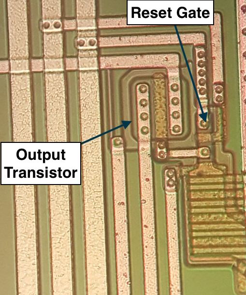
Synoptic Survey Telescope, is now known as the Simonyi Survey Telescope at the Vera Rubin Observatory, and
will be used to conduct a ten-year survey of the southern sky known as the Legacy Survey of Space and Time.
This instrument is an innovative, large, fast survey facility currently under construction at Cerro Pachon in Chile
[3]. The digital camera, also currently under construction, consists of approximately 3.2 gigapixels and is the
largest digital camera ever constructed. The camera uses fully-depleted silicon CCDs which are back illuminated
and 100 microns thick in order to optimize quantum efficiency in the near infrared. The imaging area consists
of 189 CCDs, with each CCD containing 16 imaging regions laid out in an 8x2 array. Each imaging region has
a pixel array with approximately 500x2000 10 micron square pixels, giving 16 Megapixels total. Each imaging
region also has its own independent amplifier ([4], [5]). The focal plane contains CCDs from two different vendors,
the ITL STA3800C from the University of Arizona Imaging Technology Laboratory [6], and the E2V CCD250
from Teledyne E2V [7]. However, although this code was developed and tested against these two CCDs from the
LSST project, it has already found more general use on other CCDs ([8]), and the hope is that this will continue.

This paper is divided into several sections. In Section 2, we give an overview of the simulator, describing the
basic structure of the simulation volume, how we solve the semiconductor equations, and how we treat incoming
photons. We also show a number of examples of the outputs available from the simulator. In Section 3, we review
a number of the validation tests that were performed to validate the simulation results against measured data of
different kinds, and finally we conclude.

2   Overview
The simulator performs two basic tasks, as shown in Figure 1. First, given the charges in the silicon bulk and
the boundary conditions determined by potentials applied to the silicon surface, the simulator solves Poisson’s
equation numerically to determine the potentials and electric fields in the silicon bulk. The solution to Poisson’s
equation is determined using the technique of successive over-relaxation (SOR - see for example [9]), and using
multi-grid methods (see Section 2.4) to speed convergence. In regions where there are mobile carriers (holes and
electrons) quasi-Fermi level methods are used to simultaneously solve for the potentials and free carrier densities
in the device. The electric fields are determined by numerically differentiating the electrostatic potential. In
general, the simulator only solves for the potentials and free-carrier densities in equilibrium, and is not intended
to give transient solutions. However, it is possible to repeatedly solve the equations with slight changes in initial
conditions in order to give transient results. This technique has been used to generate movies of the CCD charge
transport, as discussed in Section 3.6.

After solving for the device potentials, the second major task of the simulator comes into play. As incoming
photons enter the CCD, they generate hole-electron pairs. The electric field in the CCD separates these charges,
and the electrons propagate down to the collecting wells where they are collected, stored, and later counted.
The simulator models this carrier transport in a physically realistic way, in order to determine in which pixel
a generated carrier ends up. This is very useful for modeling pixel distortions that result from electric fields in
the device, either built-in electric fields, such as those due to “tree rings”[10], or electric fields due to collected
charges, such as those that lead to the brighter-fatter (BF) effect ([11], [12], [13], [14], [15]). Note that in an
astronomical CCD, the time between incoming charges (on the order of msec) is typically much longer than the
time required for a charge to propagate down to the bottom (on the order of nsec). Also, a single charge has little
impact on the existing potentials and fields. So it is an excellent approximation to assume that a single charge
propagates in a frozen electric field. The simulator is designed so that if multiple charges are being added, the
user can choose how often to re-solve Poisson’s equation. A comment here about the nature of the charges is in
order. The simulator is designed for N-channel CCDs (with P-type substrate), where the collected charges are
electrons, and for the rest of the paper we will make that assumption. There is no physical reason why it will
not work for P-channel CCDs (with N-type substrate), but it is not currently designed to support them. Most of
the work in adapting it for P-channel CCDs would be nomenclature related, basically interchanging the names
of holes and electrons, but adjustment of parameters like mobilities and effective masses would also be needed.
This could be done if there is demand for it.

                                                          2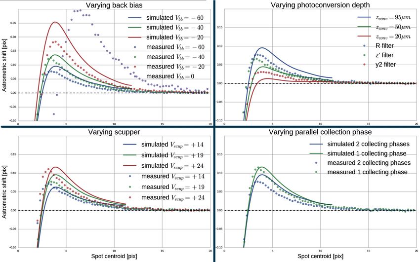
Incident Light

                                                                                                                     Back-bias
      Fixed Voltage (Back-bias) on Top        Incoming Light                                                     Poten8al sweeps
                                                                                                                   electrons to
                                                                                                                    front side.

                                                                                                                   Silicon
   Charges in bulk                                                                                                Thickness
    determined by
   bulk doping and
Channel / Channel-stop                                         Free or periodic boundary
       implants                                                   condi@ons on sides

                                                                                                                  Electrons collected
                                                                                                                   by posi8ve gates.

         Voltages on bo8om as appropriate (parallel gates)
                                                                                           - ++- ++- ++- ++- ++- ++

                              (a) Silicon volume                                                (b) Charge tracking
Figure 1: Major tasks of the Poisson CCD simulator. The left-hand figure shows the silicon volume. Given charges
in the silicon bulk and voltages applied to the silicon boundaries, one solves for the electric fields and free carrier
densities within the silicon. The right-hand figure shows incoming charges, created by incident photons, which
are propagated down through the silicon bulk to determine the number of charges in each pixel. The red and
black colors are used to delineate the charges associated with individual pixels.

2.1    Basic structure of the simulations
The simulator is written in C++, and is controlled by a text-based configuration file, which contains all of the
information about the silicon volume, pixel sizes, number of pixels, any non-pixel regions, etc. The configuration
file also defines the problem being solved. By convention the configuration file has a .cfg extension, but this is not
necessary. Appendix A lists the configuration parameters. As the simulation progresses, it writes out a number
of files. Large files containing information like potentials, charge densities, electric fields at each grid point are
written as high-density HDF5 files, having file extension .hdf5. Several smaller text files, with a .dat extension,
are written which contain information on the grids or the number of electrons in each pixel. After the simulation
has completed, easily modifiable Python scripts are used to plot out results as desired.

The simulation volume is set up on a fixed three-dimensional rectangular grid, which does not change once the
simulation has started. One begins by deciding the number of grid cells in each dimension. Because multi-grid
methods are used (see Section 2.4), the number of grid cells in each dimension must be a multiple of 32. Note
that as a convention, we refer to the side of the CCD where the circuitry is patterned as the bottom, and the side
where the incident light comes in as the top. For the LSST CCDs, which are 100 microns thick and have pixels
10 microns square, a typical resolution is to have 32 simulation grid cells per pixel, so that each grid cell is 0.31
microns. Initially, the grid was defined to be completely uniform in all three dimensions. However, for thick CCDs
like those used in the LSST, the potentials and fields change rapidly in the region near the bottom, and only very
slowly near the top. When the simulation had enough resolution to be accurate in the rapidly changing region
at the bottom, most grid cells were wasted near the top. Of course, adaptive grid methods solve this problem,
but also make the code much more complex, which defeated the purpose of having a relatively simple simulator.
The solution chosen in this work was to use a non-linear grid in the Z-dimension only. This has proven to give
high resolution where needed, without adding significant complexity to the simulation code. Figure 2 shows the
scheme. This introduces some additional partial derivatives, as discussed more in section 2.3, but these values
can be pre-calculated and this is much simpler than an adaptive grid scheme.

                                                                           3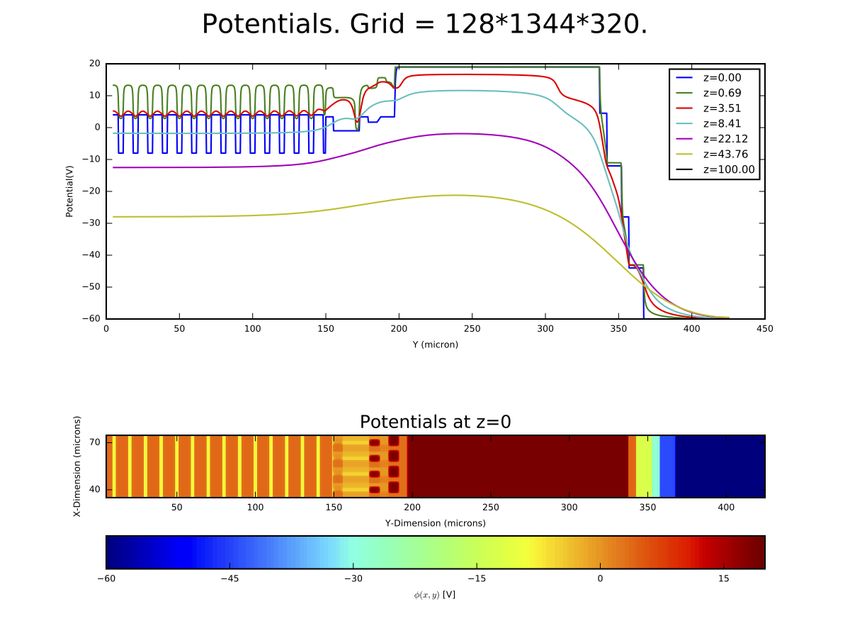
Nonlinear Z-axis
                                                       100

                                                        80

                                    ZPrime (microns)
                                                        60

                                                        40
                                                                                 NZExp = 1.00
                                                        20                       NZExp = 2.00
                                                                                 NZExp = 10.00
                                                         0                       NZExp = 100.00
                                                             0   20     40       60   80    100
                                                                      Z (microns)
Figure 2: Non-linear Z-axis scheme. The parameter NZExp allows one to have smaller Z-axis grid cells near the
bottom of the simuation volume, where the fields and charges are changing more rapidly. A value NZExp=1 is a
linear grid. The recommended value is to Use NZExp=10.0, which increases the resolution at z=0 by a factor of
10, and decreases the resolution at the top of the CCD by a factor of 10.

2.2     Setting up the initial conditions
Because the simulator is not a general purpose semiconductor solver, and is intended to model devices with a
given structure, certain assumptions are made about the structure of the CCD which simplifies building the device
structure. This is one of the reasons why this code is so much simpler than a commercial device simulator. It is
assumed that the CCD is a slab of silicon with a given thickness given by the parameter “SensorThickness”. It is
assumed that the top surface of the CCD is at a fixed voltage given by the parameter “Vbb”. The bottom surface
of the CCD has voltages specified by the various gate potentials. The doping deep in the silicon is asumed constant
with a value given by “BackgroundDoping”, although a periodic variation in this doping can be introduced using
the “TreeRing” parameters. The doping level is assumed to be modified by the introduction of implants from the
bottom side. There are several options for these doping profiles, including a square profile of a given depth or a
sum of N Gaussian profiles. Use of 1 or 2 Gaussian profiles has been found to accurately reproduce the measured
doping profiles on commercial CCDs. For more details on this, see [16].

2.2.1    Pixel arrays

Setting up the initial conditions in the periodic pixel array is straightforward, and is specified by a relatively
small number of parameters which describe the gate voltages and doping levels. Rather than go through these in
detail, the reader is referred to Appendix A or the “pixel-itl” and “pixel-e2v” examples at [2].

2.2.2    Fixed regions

Setting up the initial conditions in non-periodic regions outside the pixel array is straightforward, but more
laborious than setting up the pixel arrays. The extents, dopings, applied voltages, and quasi-Fermi levels need
to be specified for each region. At present only rectangular regions are supported. Also, it is assumed that the
same doping profiles which are used in the pixel array are used in the surrounding circuitry, so the only options
for doping profiles are the channel doping, the channel stop doping, and no doping. Examples of simulations
setting up non-periodic regions are the “edge.cfg”, “trans.cfg”, and “io.cfg” files at [2], and the results of these
simulations are detailed in Section 3.

                                                                             4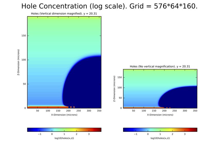
2.3   Solving for the potentials, fields, and free carrier densities
In this section we give a brief description of the methods that are used to solve Poisson’s equation on the grid.
We are trying to solve the following equation, where ϕ is the potential, ρ is the charge density, and Si is the
dielectric constant of silicon:
                                                             ρ
                                                    ∇2 ϕ =                                                    (1)
                                                            Si
Each of the partial derivatives can be discretized on a rectangular grid with grid spacing h as follows:
                                   ∂ 2 ϕi,j,k   (ϕi+1,j,k − ϕi,j,k ) − (ϕi,j,k − ϕi−1,j,k )
                                              =                                                                     (2)
                                     ∂x2                             h2
Giving for the discretized Poisson’s equation:
                                                                                                    h2
                 ϕi+1,j,k + ϕi−1,j,k + ϕi,j+1,k + ϕi,j−1,k + ϕi,j,k+1 + ϕi,j,k−1 − 6 ∗ ϕi,j,k =         ∗ ρi,j,k    (3)
                                                                                                    Si
This can be turned into an iterative equation, and basically one just iterates until convergence:
                                                                                          h2

              (n+1)   1       (n)       (n)      (n)        (n)       (n)       (n)
             ϕi,j,k = ∗ ϕi+1,j,k + ϕi−1,j,k + ϕi,j+1,k + ϕi,j−1,k + ϕi,j,k+1 + ϕi,j,k−1 −     ∗ ρi,j,k              (4)
                      6                                                                   Si
Which we write in shorthand as follows:
                                                               h2

                                                    1
                                         ϕ(n+1) =     ∗ ϕ(n)
                                                         pm  −     ∗ (ρ f + ρm )                                    (5)
                                                    6          Si
where we define:
                                   (n)        (n)         (n)         (n)         (n)         (n)
                          ϕ(n)
                           pm = ϕi+1,j,k + ϕi−1,j,k + ϕi,j+1,k + ϕi,j−1,k + ϕi,j,k+1 + ϕi,j,k−1                     (6)
and we have split ρ into a fixed charge density ρf and a mobile charge density ρm . However, ρm is a highly
nonlinear function of the potential ϕ, as described below. In quasi-equilibrium, the drift current JE and the
diffusion current JD are equal, giving a net current of zero, so we can write (see Sze [17], for example):

                                                    dϕ                    dn
                                          JE = qe µn n  = −JD = −qe Dn                                           (7)
                                                     dx                   dx
Here qe is the electron charge, µn is the electron mobility, n is the electron density in electrons per unit volume,
and Dn is the electron diffusion coefficient. This gives:
                                                                     dn
                                                     µn dϕ = −Dn                                                    (8)
                                                                      n
We also know from the Einstein relations that the mobility and diffusion coefficent are related by the following
equation, where k is Boltzmann’s constant and T is the absolute temperature::
                                                         µn   qe
                                                            =                                                       (9)
                                                         Dn   kT
so, integrating both sides:
                                              qe ϕ
                                                   = log (n) + C                                        (10)
                                              kT
We take the constant of integration into the exponential and define the quasi-Fermi level ϕF in terms of the
intrinsic carrier density ni , giving:
                                                       qe (ϕ − ϕF )
                                          n = ni exp                                                    (11)
                                                            kT
So we need to solve the following equation for ϕ, where ϕF is a constant:

                                     2     1                     qe (ϕ − ϕF )
                                   ∇ ϕ=         ρf + qe ni exp                                                     (12)
                                          Si                         kT

                                                                5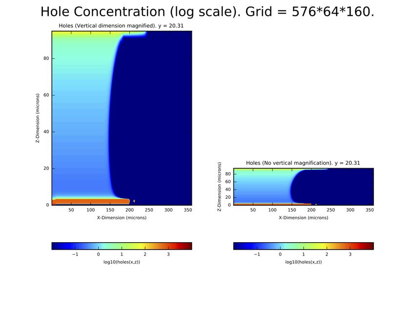
which, when discretized is:
                                                                                                !!
                                  1           h2         h2 qe ni             qe ϕ(n+1) − ϕF
                        ϕ(n+1)   = ∗    ϕ(n)
                                         pm −     ∗ ρf −          exp                                             (13)
                                  6           Si          Si                      kT

Because of the strong non-linearity, simply iterating is numerically unstable. The method that works, described
in detail by Rafferty, et.al. [18] and buillding on the work of Gummel ([19]), is to take this last equation as a
non-linear equation for ϕ(n+1) in terms of ϕn and run a Newton’s method “inner loop” to find ϕ(n+1) at each grid
point. Then we iterate to convergence as before. This allows us to simultaneously solve for the potential and the
carrier density. Of course, we just described the electron density here, but there is a similar equation for holes, but
with opposite signs. Figure 3 shows an example of varying ϕF on the solution. Note that the quasi-Fermi level is
constant in each region containing mobile carriers. In the CCD, each collecting well contains a different number
of mobile carriers, so ϕF is constant in each well, but is different from well to well. However, when simulating the
device, instead of knowing the value of ϕF , we typically know the number of electrons in each well. So how do
we translate from the known number of electrons to the unknown value of ϕF ? The code provides two methods,
selected by the value of the parameter “ElectronMethod”. With this parameter set to 1, a test simulation is run
where the parameter ϕF (called QFe in the code) is varied through a range. For each value of QFe, we integrate
over a pre-determined region to count the number of electrons in the well, building a look-up table of the number
of electrons vs QFe. The results for a few values of QFe are shown in Figure 3. Then the code interpolates to
determine the value of QFe which gives the appropriate number of electrons. In practice one can get close to the
desired number of electrons, but the non-linearity causes variations from the desired number, so a second method
was developed. When “ElectronMethod” has a value of 2, what is done is to place the correct number of electrons
in the well, uniformly distributed in the center of the well. The code then moves the electrons around until the
value of QFe is constant in the well. This allows one to get the correct number of electrons in the well without
needing to know the value of the quasi-Fermi level.

There is one more complication. As discussed in Section 2.1, a non-linear Z-axis is used to concentrate grid cells
in the bottom region where the potentials and charge densities are changing most strongly. In principle, any
smooth funcation can be used for the Z-axis mapping. Here we chose an easily differentiable polynomial function
of the following form, where z is the linear z coordinate, and zp is the non-linear coordinate, which is the actual
value used in solving and plotting. Here TSi is the silicon thickness, and NZExp is a user-defined constant that
controls the non-linearity, as described in Figure 2.

                                                              (NZExp+1.0)/NZExp
                       zp = −TSi ∗ (NZExp − 1.0) ∗ (z/TSi )                             + NZExp ∗ z;              (14)

The non-linear z-axis modifies Poisson’s equation from:

                                                      ∂2ϕ ∂2ϕ ∂2ϕ
                                             ∇2 ϕ =       +     + 2                                               (15)
                                                      ∂x2   ∂y2  ∂z
to:                                                                      2
                                            ∂2ϕ ∂2ϕ ∂2ϕ            ∂z0            ∂ϕ ∂ 2 z0

                                   ∇2 ϕ =       +     + 2                     +                                   (16)
                                            ∂x2   ∂y2  ∂z          ∂z             ∂z0 ∂z2
In practice, the additional partial derivatives can be pre-computed, so this is simply accounted for in the discretized
equations and has only a minor impact on the speed of iteration.

                                                          6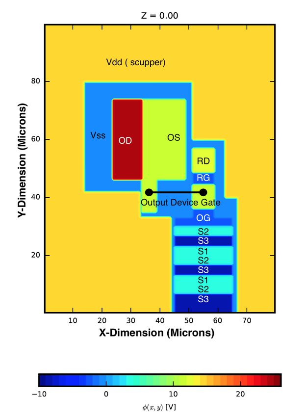
15
                                     QFe = 4.87                       15
                                                                             QFe = 7.91                       15
                                                                                                                    QFe = 10.47                       15
                                                                                                                                                            QFe = 11.15

                              10                                      10                                      10                                      10
         φ(x,y,z) [V]

                               5                                       5                                       5                                       5

                               0                                       0                                       0                                       0
                                          300000 electrons                        100000 electrons                        10000 electrons                         1000 electrons
                                          QFe                                     QFe                                     QFe                                     QFe
                               5                                       5                                       5                                       5
                                0.0 0.5 1.0 1.5 2.0 2.5 3.0 3.5 4.0     0.0 0.5 1.0 1.5 2.0 2.5 3.0 3.5 4.0     0.0 0.5 1.0 1.5 2.0 2.5 3.0 3.5 4.0     0.0 0.5 1.0 1.5 2.0 2.5 3.0 3.5 4.0

                              80
                                     QFe = 4.87                       80
                                                                             QFe = 7.91                       80
                                                                                                                    QFe = 10.47                       80
                                                                                                                                                            QFe = 11.15
                              60                                      60                                      60                                      60
      ρ(x,y,z)/²Si [V/um2 ]

                              40                                      40                                      40                                      40
                              20                                      20                                      20                                      20
                               0                                       0                                       0                                       0
                              20                                      20                                      20                                      20
                              40                                      40                                      40                                      40
                              60          Fixed charge                60          Fixed charge                60          Fixed charge                60          Fixed charge
                                          300000 electrons                        100000 electrons                        10000 electrons                         1000 electrons
                              80                                      80                                      80                                      80
                                0.0 0.5 1.0 1.5 2.0 2.5 3.0 3.5 4.0     0.0 0.5 1.0 1.5 2.0 2.5 3.0 3.5 4.0     0.0 0.5 1.0 1.5 2.0 2.5 3.0 3.5 4.0     0.0 0.5 1.0 1.5 2.0 2.5 3.0 3.5 4.0
                                     Z-(microns)                             Z-(microns)                             Z-(microns)                             Z-(microns)

Figure 3: Impact of varying ϕF (called QFe in the code, with units of Volts) on the potential and electron density.

2.4    Multi-grid methods
It is well known that multi-grid methods speed convergence of solutions to Poisson’s equation by getting correct
solutions to the long-wavelength modes at a coarser grid where convergence is much more rapid. There is a
wealth of literature on the subject, and Briggs [20] or Press [21] give excellent summaries. The basic idea is
shown in Figure 4. In practice in this code, we have adopted a simpler method. Rather than use “Restriction”
to propagate the boundary conditions down to the coarser grid, we simply set up the boundary conditions on
all of the sub-grids at the outset of the problem. In addition, we have found that there is little value in running
coarser grids than 403 , because at this resolution the problem converges very rapidly. So for a typical problem
which has perhaps 3203 grid cells, we define the finest grid and three subgrids, with the coarsest grid having 403
grid cells. We then set up the boundary conditions on all of the subgrids, iterate the coarsest grid, “Prolongate”
the solution up to the next grid, and continue until we have reached the finest grid.

                                                                                                          7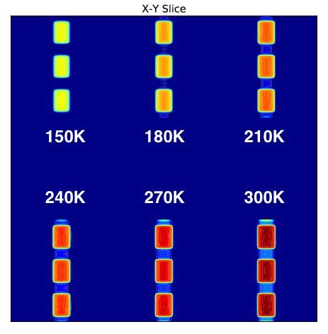
Restric5on
Problem
at
Propagate
fine
grid
Boundary
Condi5ons
to
coarser
grid
Prolonga5on
Iterate
to
Propagate
Iterate
to
solve
problem
coarse
solu5on
solve
problem
on
finer
grid
to
finer
grid
on
coarse
grid
Mul1-‐Grid
V-‐Cycle
3203
3203
1603
1603
803
803
403
403
Restric1on
203
203
Prolonga1on
103
53
Figure 4: Basic idea of multi-grid methods. Long wavelength modes are solved on a coarser grid, which is then
propagated to a finer grid (“Prolongation”), where more iterations are performed to find the fine details of the
solution.
At this point it is appropriate to discuss the problem of convergence. Convergence of the SOR algorithm is
notoriously slow. Multi-grid methods help a great deal, however, care must still be taken to ensure that the
solution has converged adequately for your problem. The parameter “ncycle” controls the number of iterations
taken at the finest grid. Each coarser grid increases the number of iterations by a factor of 4. So for example, a
8typical problem like one of the “pixel” examples, which has ncycle=128, the coarsest grid has 1/8 the resolution,
and will run 128 × 43 = 8192 SOR cycles at the coarsest grid. Figures 5 and 6 show the convergence of a typical
problem. For most problems, a value of ncycle=64 is adequate. The problems most dependent on accurate
convergence have proven to be the pixel distortion simulations like those in Section 3.1. Since we are dealing
with very small deviations in the pixel shapes due to the BF effect, it is important to make sure the results have
converged.
Convergence Tests
Phi-Collect Gate Phi-Collect Gate
15
10
(x, y, z) [V]
(x, y, z) [V]
10
0
5
10
0
0 2 4 0 5 10 15
Z-Dimension (microns) Z-Dimension (microns)
Phi-Chan Stop Phi-Chan Stop
Grid 0
0 Grid 1 5
(x, y, z) [V]
(x, y, z) [V]
20 Grid 2
Grid 3 0
40
60 5
0 50 100 0 5 10 15
Z-Dimension (microns) Z-Dimension (microns)
Figure 5: Convergence of the multi-grid subgrids. The parameter “ncycle” has a value of 64 in these plots. Each
subgrid is a factor of two coarser than the preceding grid.
9Phi-Collect Gate Phi-Collect Gate
10 ncycle=4
10 0 ncycle=16
φ(x, y, z) [V]
φ(x, y, z) [V]
10 ncycle=64
5 20 ncycle=256
30
0 40
50
5
0 1 2 3 4 0 50 100
Z-Dimension (microns)
13
Z-Dimension (microns)
24
φ(x, y, z) [V]
φ(x, y, z) [V]
12
26
11
28
10
0.5 1.0 1.5 2.0 38 39 40 41 42
Z-Dimension (microns) Z-Dimension (microns)
Figure 6: Convergence of the highest resolution grid as a function of the parameter “ncycle”. For most uses a
value of 64 is adequate.
2.5 Modeling carrier transport
The basic scheme for modeling carrier transport is shown in Figure 7. Electrons are assumed to have lattice
collisions on a time scale τ , which is on the order of picoseconds. At each collision, the electron is assumed to
pick up a thermal velocity Vth which is in a random direction. In addition to this thermal velocity, it also has
a drift velocity given by Vdrift = µE, where the mobility µ(E, T) is calculated as a function of electric field and
temperature using the mobility model of Jacobini [22]. These two velocities are added vectorially and it travels
in this direction at this velocity for a time δt until the next collision, and this continues until the electron reaches
the bottom. The electron path is logged in the * Pts.dat file. If the parameter “LogPixelPaths” is zero, only the
initial and final positions are logged. If this parameter is one, the entire path is logged. The thermal velocity has
a multiplier (“DiffMultiplier”) which can be used to tune the amount of diffusion. If this is set to zero, diffusion
is turned off, with the impact as shown in Figure 8. A value DiffMultiplier = 2.30 has been found to accurately
reproduce the amount of diffusion seen in Fe55 data (see Section 3.2). Since the value of m∗e in the code is the
bare electron mass, this value is equivalent to an electron effective mass of about 0.19. This is somewhat low, as
Green [23] finds a value of 0.27. This value of DiffMultiplier is easily adjusted by the user, however.
The initial electron locations in X and Y can be determined in a number of ways, as determined by the “Pixel-
BoundaryTestType” parameter. These include an equally spaced grid, a Gaussian spot, a random location within
a boundary, an Fe55 event, or reading in a list of locations. The starting location in Z can either be specified, or
calculated given a filter band.
10Vth δt µE δt
µE δt Vth δt Mobility: µ(E, T ) calculated from Jacobini model [22]
cm2 V
µ ≈ 1500 V−sec at E = 6000 cm
µE δt
Vth δt Collision time:
m∗
Each (me step: τ = qee µ
µE δt Dri1 velocity of µ*E τ typically about 0.9 ps.
Thermal velocity of Vtδt
in drawn from
a random exponential
direc(onq distribution with mean of τ
Vth δt Vth = DiffMultiplier 8kT
πm∗
e
.
Vdrift = µE
Each thermal step in a random direction in 3 dimensions.
.
Typically about 1000 steps to propagate to the collecting well.
.
Figure 7: Diffusion model
CCD Pixel Plots.PixelGrid
100
= 320*320*320.
Boundaries
CCD Pixel Plots.PixelGrid = 320*320*320.
Boundaries 100
90 90
80 80
70 70
Y(microns)
Y(microns)
60 60
50 50
40 40
30 30
Electron Path Plot - Vertical Zoom
20
10
Electron
= 1 Path Plot - Vertical Zoom 20
10
10 20 30 40 50 60 70 80 90 100 10 20 30 40 50 60 70 80 90 100
X(microns) X(microns)
100 100 100 100
Z(microns)
Z(microns)
Z(microns)
Z(microns)
80 80 80 80
60 60 60 60
40 40 40 40
20 20 20 20
0 0 0 0
20 40 60 80 100 20 40 60 80 100 20 40 60 80 100 20 40 60 80
X (microns) Y (microns) X (microns) Y (microns)
Diffusion turned off Realistic Diffusion
Figure 8: Impact of diffusion on electron paths of a Gaussian spot with a sigma of 1 pixel. With diffusion turned
off, the electrons simply propagate down and end up in the same pixel they started. With realistic diffusion, the
electrons can cross pixel boundaries.
112.6 Example outputs
Once the simulation has run, the potential, electric fields, and charge carrier densities are available throughout
CCD Charge Collection. Grid = 320*320*320.
the simulation volume. What one chooses to visualize depends on the problem being studied. Here we have
chosen three examples (Figures 9, 10, and 11) of the type of data which is available.
Phi, z = 0.0 Rho, z = 0.00 - 2.68
70 8.00 70 14
Channel Stops
65 5.33 65 7
Y-Dimension (microns)
Y-Dimension (microns)
Channel
(x, y, z)/ Si [V/ 2]
60 2.67 60 0
Barrier Gate
(x, y, z) [V]
7
55 Collect Gates 0.00 55
14
50 2.67 50
21
45 5.33 45
28
40 8.00 40
35
35 35
40 50 60 70 40 50 60 70
X-Dimension (microns) X-Dimension (microns)
Phi, z = 1.18 Phi, z = 2.68
18 18
70 70
12 12
65 65
Y-Dimension (microns)
Y-Dimension (microns)
60 6 60 6
(x, y, z) [V]
(x, y, z) [V]
55 0 55 0
50 6 50 6
45 45
12 12
40 40
18 18
35 35
40 50 60 70 40 50 60 70
X-Dimension (microns) X-Dimension (microns)
Figure 9: A summary of the region near the bottom of the ITL STA3800C CCD. The upper left shows the applied
parallel gate voltages, and the upper right shows a 2D projection of the fixed charges. The lower two plots show
the potential at two different z-values above the bottom of the CCD. Here the center pixel has 100,000 electrons
and the surrounding pixels are empty.
121D Potential and Charge Density Slices. Grid = 320*320*320.
25
Phi-Collect Gate Phi-ChanStop Phi-Barrier Gate
10.0 10.0
20 7.5 7.5
(x, y, z) [V]
15 5.0 5.0
2.5 2.5
10
0.0 0.0
5 2.5 2.5
5.0 5.0
0 100K electrons CollectGate
Empty Well 7.5 Barrier Gate 7.5
5 10.0 10.0
0 1 2 3 4 0 2 4 6 8 10 0 1 2 3 4
250
Rho-Collect Gate 100
Rho-ChanStop 250
Rho-Barrier Gate
Fixed charge
(x, y, z)/ Si [V/ 2]
200 100K electrons 75 200
Empty well 50
150 150
25
100 100
0
50 25 50
0 50 Fixed charge 0
75 Holes Collect Gate Fixed charge
50 Holes Barrier Gate 50 Holes
100
0 1 2 3 4 0 2 4 6 8 10 0 1 2 3 4
Z-Dimension (microns) Z-Dimension (microns) Z-Dimension (microns)
Figure 10: A set of vertical 1D profiles of potential and charge density at various locations of the ITL STA3800C
CCD. Again, the center pixel has 100,000 electrons and the surrounding pixels are empty. The sharp discontinuities
near the left edge of the plots are at the Si/SiO2 interface where the device silicon begins. This is at a z-coordinate
of about 0.69 in the channel region and 1.09 in the channel stop region.
13Fixed Charge Distribution Mobile Charge Distribution
X-Y Slice Y-Z Slice Y-Cut X-Y Slice Y-Z Slice Y-Cut
65.0 65.0
62.5 62.5
60.0 60.0
57.5 57.5
Y (Microns)
Y (Microns)
55.0 55.0
52.5 52.5
50.0 50.0
47.5 47.5
45.0 45.0
X-Z Slice 2 1 Charge Density
0 X-Z Slice 2 1 0
Charge Density
0
(arb. units) (arb. units)
2
Z-Cut 2
Z-Cut
(arb. units)
(arb. units)
Log Charge
Log Charge
1 0 Density 1 0
Density
2 2
0
X-Cut 0
X-Cut
Charge Density
Charge Density
4 4
(arb. units)
(arb. units)
2 1 0 2 1 0
0 Z ( Microns) Z ( Microns)
+ Charge in Red + Charge in Red
-Charge in Blue 0 - Charge in Blue
45.0 47.5 50.0 52.5 55.0
X (Microns)
57.5 60.0 62.5 65.0
Oxide in yellow 45.0 47.5 50.0 52.5 55.0
X (Microns)
57.5 60.0 62.5 65.0
Oxide in yellow
Gates in green Gates in green
Figure 11: A set of 2D projections of the distribution of fixed and mobile charges near the bottom of the ITL
STA3800C CCD. Again, the center pixel has 100,000 electrons and the surrounding pixels are empty. The Si/SiO2
interface, where the device silicon begins, is at a z-coordinate of about 0.69 in the channel region and 1.09 in the
channel stop region.
3 Validation with measured data
To successfully model a CCD, an accurate physical characterization of the CCD is needed. Details such as dopant
densities, layer thicknesses, and physical dimensions need to be known, at least approximately. For modeling the
CCDs from the two vendors which will be used in the LSST camera, we obtained detailed physical measurements,
which have been described in [16]. This has helped to make the simulations described in the next few sections
as physically realistic as possible. Most of the plots in this section can be reproduced using the examples at the
Poisson CCD code site at [2].
Regarding the parameters used in the simulations, there has been optimization of the numeric parameters, such as
grid size, number of iterations, successive over-relation factor, etc. to ensure convergence and accuracy. However,
the physical parameters, such as physical dimensions, voltages, doping levels, oxide thicknesses, etc. have all been
directly measured. In particular, these parameters have not been tuned to improve the fit with measured data
shown in the following examples.
3.1 Pixel distortions and pixel-pixel covariances
As has been extensively discussed in the literature ([11], [12], [13], [14]), as charge builds up in the central region
of bright objects, the stored charge repels additional incoming charge and broadens the profile of these objects.
The impact of the stored charge on the pixel shapes can be determined by measuring the pixel-pixel covariances
on a large number of flat images ([11], [15]). These covariances are calculated from a large number of flat pairs
of varying intensity (see [15] for example) as:
14P ¯ − f¯)
I,J (fI,J − f )(fI+i,J+j
Ci,j = (17)
f¯2 (Npix − 1)
where fi,j is the difference in flux between the two flats at pixel i,j, and Npix is the number of pixels summed over.
We have generated this data on a large number of flat pairs on LSST CCDs, measured on the UC Davis LSST
beam simulator ([24], [14]), and would like to compare these results to simulations. For a dataset of 100 flat
pairs, each with 16 million pixels with an average signal level of 50,000 electrons, this is approximately 1014
electrons. Directly simulating this data is out of the question. However, we have found a simple way to run
a single simulation which reproduces the measured pixel covariances. In order to do this, we first simulate a
situation where one pixel has a fixed amount of charge (typically 100,000 electrons), and all surrounding pixels
are empty. After solving for the potential and resulting electric field, we can track electrons down through the
silicon. As the electrons travel down through the silicon under the influence of the electric field, they eventually
end up in one of the collecting wells. A binary search is used to find the bifurcation points where electrons on
one side of the bifurcation point end up in one pixel, and electrons on the other side of the bifurcation point end
up in an adjacent pixel. This binary search is performed with diffusion turned off in order not to introduce a
stochastic element into the electron paths. These bifurcation points are identifed as the pixel boundaries. This
allows us to characterize the distortion in the pixel boundaries which results from the central pixel charge. A
typical result of this process is shown in Figure 12. The number of vertices used to define the distorted pixel
shapes is an adjustable parameter. A minimum of 12 vertices is needed to adequately define the distortion (4
corners plus 2 points per edge). The distorted pixels shown in Figure 12 and used in Figure 13 were simulated
with a total of 132 vertices (4 corners plus 32 points per edge). The distorted pixel shapes which result are what
gives rise to the BF effect, with the central pixel losing area, which is gained by the surrounding pixels.
15Pixel Vertices: 100000 e-
80
100.0432 100.0853 100.1231 100.0853 100.0432
Electron Charge Distribution 70
X-Y Slice Y-Z Slice Y-Cut
65.0
100.0826 100.3513 101.5733 100.3517 100.0819
62.5
60.0 60
57.5
Y (Microns)
55.0
100.1136 100.6512 91.0753 100.6515 100.1133
52.5
50
50.0
47.5
100.0827 100.3380 101.5774 100.3376 100.0823
45.0
X-Z Slice 4 2 0
Charge Density 40
0
(arb. units)
4
Z-Cut
100.0432 100.0853 100.1225 100.0855 100.0430
(arb. units)
Log Charge
2 0
Density
2
0
X-Cut
30
Charge Density
4
(arb. units)
2 1 0
Z ( Microns)
0
45.0 47.5 50.0 52.5 55.0 57.5 60.0 62.5 65.0
Oxide in yellow
30 40 50 60 70 80
X (Microns) Gates in green
(a) Charge packet with 100,000 electrons (b) Pixel distortion from the central charge packet
Figure 12: Simulation of pixel distortions in an ITL chip when the central pixel contains 100,000 electrons and the
surrounding pixels are empty. X and Y are the lateral dimensions of the CCD, and Z is the thickness dimension.
The CCDs are 100 microns thick. These distortions are obtained by solving Poisson’s equation for the potentials
in the CCD, then tracking electrons down and using a binary search to determine the pixel boundaries as described
in the text. As expected, the central pixel loses area and the surrounding pixels all gain area. Note that the loss
in area of the central pixel is greater than the sum of the area gains of the surrounding pixels because there are
more distant pixels which are not plotted here and which also gain area.
We find that the area distortions which result accurately capture the measured pixel-pixel covariances. Figure
13 shows the agreement between the measured pixel-pixel covariances on flat field images and the simulated area
distortions, as measured and as simulated on LSST CCDs from both CCD vendors. The agreement is quite good.
The asymmetry of the nearest neighbor pixels is correctly modeled, and the simulated values agree with the
measurements within the statistical errors. These simulations are run with the “pixel-itl.cfg” and “pixel-e2v.cfg”
examples at [2]. More details on these measurements and simulations are given in [14] and [25].
1610 5 Covariance Matrix
C00: Meas = -1.044e-06, Sim = -9.222e-07 Positive Sims
C01: Meas = 1.761e-07, Sim = 1.704e-07
C10: Meas = 7.245e-08, Sim = 7.085e-08 Negative Sims
Covariance or Area/Area
10 6
C11: Meas = 4.347e-08, Sim = 3.561e-08 Positive Meas
2/DOF = 1.22
Negative Meas
10 7
10 8
10 9
10 10
100 101 102
i + j2
2
(a) ITL Detector
10 5 Covariance Matrix
C00: Meas = -1.68e-06, Sim = -1.598e-06 Positive Sims
C01: Meas = 2.747e-07, Sim = 2.675e-07
C10: Meas = 9.828e-08, Sim = 8.489e-08 Negative Sims
Covariance or Area/Area
10 6
C11: Meas = 6.433e-08, Sim = 6.518e-08 Positive Meas
2/DOF = 1.43
Negative Meas
10 7
10 8
10 9
10 10
100 101 102
i + j2
2
(b) E2V Detector
Figure 13: Covariance measurements and simulations. The simulated pixel area distortions (see Figure 12)
accurately determine the measured pixel-pixel covariances as measured on flat pairs. The circles are the measured
covariances, as extracted by the code in the LSST image reduction pipeline as described in the text. The crosses
are the fractional area distortions as simulated by the Poisson CCD code and shown in Figure 12. The leftmost
point (the central pixel) has been shifted to an X-axis value of 0.8 to allow plotting it on this log-log plot. Both
the E2V and ITL simulations have been informed by physical analysis of both chips, including SIMS dopant
profiling and measurements of physical dimensions [16]. Both the covariance measurements and the simulations
have been normalized to the distortion caused by one electron. The asymmetry of the nearest neighbor pixels is
correctly modeled, and the simulated values agree with the measurements within the statistical errors.
173.2 Diffusion modeling and Fe55 tests
CCDs are routinely characterized by exposing the CCD to an Fe55 source. (see [26], for example). The radioactive
decay produces X-rays with a known energy, with the Kα peak being the strongest peak, typically producing
1620 hole-electron pairs when photoelectrically absorbed in the silicon. These carriers then propagate down to
the collecting wells, where they are collected and counted. Because of diffusion, the carriers, which are initially
produced in a small volume, spread out and occupy several pixels. To simulate these events, a special module
was written. Normally photoelectrons propagate one at a time, without influence from neighboring carriers. But
the carriers produced in the Fe55 event are produced in a short time, so interactions between the carriers might
be important. The code takes the like carrier repulsion and opposite carrier attraction into account, and the
parameters “Fe55ElectronMult” and “Fe55HoleMult” can be used to turn off or modify this interaction if desired.
Figure 14 shows a typical event, and Figure 15 shows stacked pixel maps compared between measurements and
simulations. The spread of the charge cloud due to diffusion is well modeled. This simulation is run with the
“fe55.cfg” example at [2].
Figure 14: This shows a simulation of a typical Fe55 event in an ITL device. Electrons are shown in blue (moving
downward) and holes in red(moving upward). The left panel is a slice in the serial direction, and the right panel
is a slice in the parallel direction. Only a small fraction of the 1620 incident hole-electron pairs are plotted here.
18Stacked Fe55 events - ITL, 554913 hits Stacked Fe55 events - E2V, 739899 hits
1024 Simulated events - DiffMultiplier = 2.30 1024 Simulated events - DiffMultiplier = 2.30
0.6 1.0 1.9 1.0 0.6 0.7 0.9 1.7 0.9 0.7
2 +/- 0.1 +/- 0.1 +/- 0.2 +/- 0.1 +/- 0.0 2 +/- 0.0 +/- 0.1 +/- 0.1 +/- 0.1 +/- 0.0
0.0 0.6 1.9 0.6 0.0 0.0 0.7 2.3 0.7 0.0
+/- 0.0 +/- 0.1 +/- 0.1 +/- 0.1 +/- 0.0 +/- 0.0 +/- 0.1 +/- 0.1 +/- 0.1 +/- 0.0
0.9 43.7 176.6 43.6 0.9 1.0 44.2 177.1 44.0 1.0
1 +/- 0.0 +/- 0.9 +/- 1.2 +/- 0.9 +/- 0.1 1 +/- 0.0 +/- 0.5 +/- 0.7 +/- 0.3 +/- 0.0
0.7 47.6 173.5 42.2 0.5 0.6 44.1 182.9 50.0 0.6
+/- 0.1 +/- 2.2 +/- 5.0 +/- 2.0 +/- 0.1 +/- 0.1 +/- 2.1 +/- 5.2 +/- 2.3 +/- 0.1
1.7 178.4 711.1 178.4 1.7 1.8 178.4 701.8 178.1 1.8
0 +/- 0.1 +/- 1.1 +/- 7.1 +/- 0.8 +/- 0.1 0 +/- 0.1 +/- 1.0 +/- 2.5 +/- 0.9 +/- 0.1
2.0 172.8 729.1 158.6 1.8 1.9 157.0 725.6 168.4 1.9
+/- 0.1 +/- 5.1 +/- 6.5 +/- 4.8 +/- 0.1 +/- 0.1 +/- 4.7 +/- 6.8 +/- 4.8 +/- 0.1
0.9 43.5 176.5 43.7 0.9 1.0 44.1 177.1 44.1 1.0
1 +/- 0.0 +/- 1.0 +/- 1.0 +/- 0.8 +/- 0.0 1 +/- 0.0 +/- 0.4 +/- 0.9 +/- 0.5 +/- 0.1
0.5 43.4 165.0 41.4 0.5 0.6 42.5 164.8 41.6 0.5
+/- 0.1 +/- 2.0 +/- 5.0 +/- 2.0 +/- 0.1 +/- 0.1 +/- 2.0 +/- 4.9 +/- 1.9 +/- 0.1
0.6 0.9 1.7 0.9 0.6 0.6 0.9 1.7 0.9 0.7
2 +/- 0.1 +/- 0.0 +/- 0.1 +/- 0.1 +/- 0.1 2 +/- 0.0 +/- 0.0 +/- 0.1 +/- 0.1 +/- 0.0
0.0 0.5 1.8 0.6 0.0 0.0 0.7 2.0 0.5 0.0
+/- 0.0 +/- 0.1 +/- 0.1 +/- 0.1 +/- 0.0 +/- 0.0 +/- 0.1 +/- 0.1 +/- 0.0 +/- 0.0
2 1 0 1 2 2 1 0 1 2
(a) ITL device - χ2 /DOF = 1.4 (b) E2V device - χ2 /DOF = 2.1
Figure 15: Comparison of Fe55 event stacked pixel maps between measurement and simulation for both ITL
and E2V devices. The numbers in each pixel are the average number of electrons in each pixel, when the event
is centered on the center pixel(2,2). The measurements (top, in green) are a stack of several hundred thousand
events, and the errors of the measurements are one sigma values of the 16 amplifiers on one CCD. The simulations
(bottom, in red) are a stack of 1024 simulated events, and the errors are statistical. The spread of the charge
cloud due to diffusion is well modeled.
3.3 Saturation and blooming
A large number of simulations have been run to better understand saturation and blooming in the ITL STA3800C
device. These simulations have been very helpful to understand the physics of the device, because in the simulator
one can get information which is simply not accessible to measurement. Figure 16 shows the distinction between
the “bloomed full well” condition, where charge begins to bloom above the charge storage regions, and the
“surface full well” condition, where charge blooms along the silicon surface. This effect is discussed in detail in
Janesick [26]. The simulations in Figures 17 and 18 reproduce these conditions, and these simulations illustrate
the difference between these conditions. Measurements of saturated spots in the surface full well condition, shown
in Figure 19 also show that in the surface full well condition, charge is lost to traps at the silicon-silicon dioxide
interface. Thus it is apparent that the surface full well condition is to be avoided.
We can go further and quantitatively reproduce measurements of the onset of saturation as a function of parallel
low and high voltages, as shown in Figure 20. By quantifying the barrier height between the storage wells, we
show that saturation occurs when the barrier height drops below a certain value. The fit is good except in the
strong surface full well condition, because the charge loss that occurs is not included in the simulations. It would
be possible to modify the simulations to include this effect, but since the surface full well condition is to be
19avoided, this was deemed to be not worth the effort.
(a) Surface full well vs bloomed full (b) Similar measurements on the ITL STA3800C
well. Reproduced from [26].
Figure 16: As discussed in Janesick [26], depending on the parallel gate high voltage, saturation can occur either
at the silicon surface or above the collecting wells. This is illustrated in Figures 17 and 18. The difference in
shape in the surface full well condition in the two cases is not well understood at present.
20Electron Charge Distribution 1D Potential and Charge Density Sl
X-Y Slice Y-Z Slice Y-Cut, X = 35.16 15
Phi-Collect Gate 10
Phi-ChanSto
50
10 5
45
φ(x, y, z) [V]
5 0
40
0 5
Y (Microns)
35 250K electrons CollectGate
Empty Well Barrier Gate
5 10
0.0 0.5 1.0 1.5 2.0 2.5 3.0 3.5 4.0 0 2 4 6
30
80
Rho-Collect Gate Rho-ChanSto
25 40
60
ρ(x, y, z)/²Si [V/um 2 ]
40
20
20
20
3000
2500
2000
1500
1000
500
X-Z Slice Z-Cut
Log Charge Density
1 Charge Density 0 0
0
1 20
2 20
3 40
4 Fixed charge Fixed charge
2 1 0 60 250K electrons Holes Collect Gate
Z ( Microns) 40
X-Cut, Y = 35.16 Empty well Holes Barrier Gate
3000 Z-Axis has a 2.0X Scale Multiplier 80
Charge Density
2500 0.0 0.5 1.0 1.5 2.0 2.5 3.0 3.5 4.0 0 2 4 6
2000
1500
1000
Oxide in yellow, Gates in green Z-Dimension (microns) Z-Dimension (mic
500
0
20 25 30 35 40 45 50
X (Microns)
Figure 17: Simulation of the bloomed full well condition. Each of the three pixels contains 250,000 electrons, and
the parallel high voltage is 2.0V. The yellow circle shows where charge is blooming above storage wells. The red
circle shows that the potential in the storage well is still above that at the gate interface, keeping charge away
from the surface.
21Electron Charge Distribution 1D Potential and Charge Density Sl
X-Y Slice Y-Z Slice Y-Cut, X = 35.16 15
Phi-Collect Gate 10
Phi-ChanSto
50
10 5
45
φ(x, y, z) [V]
5 0
40
0 5
Y (Microns)
35 250K electrons CollectGate
Empty Well Barrier Gate
5 10
0.0 0.5 1.0 1.5 2.0 2.5 3.0 3.5 4.0 0 2 4 6
30
80
Rho-Collect Gate Rho-ChanSto
25 40
60
ρ(x, y, z)/²Si [V/um 2 ]
40
20
20
20
3000
2500
2000
1500
1000
500
0
X-Z Slice Z-Cut
Log Charge Density
1 Charge Density 0 0
0
1 20
2 20
3 40
4 Fixed charge Fixed charge
2 1 0 60 250K electrons Holes Collect Gate
Z ( Microns) 40
X-Cut, Y = 35.16 Empty well Holes Barrier Gate
3000 Z-Axis has a 2.0X Scale Multiplier 80
Charge Density
2500 0.0 0.5 1.0 1.5 2.0 2.5 3.0 3.5 4.0 0 2 4 6
2000
1500
1000
Oxide in yellow, Gates in green Z-Dimension (microns) Z-Dimension (mic
500
0
20 25 30 35 40 45 50
X (Microns)
Figure 18: Simulation of the surface full well condition. Each of the three pixels contains 250,000 electrons, and
the parallel high voltage is 6.0V. The yellow circle shows where charge is blooming along the silicon surface. The
red circle shows that the potential in the storage well is now below that at the gate interface, causing added
charge to be added at the surface. The cyan circle shows the surface spike of added charge.
22(a) Spot images at different parallel high voltages.
(b) Parallel high voltage of 2.5V - bloomed full well. (c) Parallel high voltage of 6.0V - surface full well.
Figure 19: Spot images in the bloomed full well and surface well conditions. In the top panel, we see that we
begin to see “trailing” when we enter the surface full well condition, because charges are trapped at the silicon
surface. In the bottom two panels, the vertical dotted line indicates the onset of saturation. In the bottom left
panel, we see that in the bloomed full well condition the total charge in the saturated spot increases linearly with
flux and no charge is lost. In the bottom right panel, we see that in the surface full well condition, charge begins
to be lost as we enter saturation. We believe this charge recombines at surface traps at the silicon-silicon dioxide
interface.
23Barrier Height
(a) Simulation with increasing charge, (b) Quantification of barrier height.
showing onset of blooming.
Saturation Curve - ITL STA3800 - 029
900 Interwell Barrier Height vs Pixel Charge 600000
Vph = 1.0 Meas:Vpl = -2V
800 Vph = 2.0 Meas:Vpl = -4V
500000 Simulations are large stars Meas:Vpl = -6V
700 Meas:Vpl = -8V
600 400000
Peak Signal(Electrons)
Barrier Height (mV)
500
300000
400
300 200000
200
100000
100
3*kT/q
0 0
140000 160000 180000 200000 220000 240000 260000 280000 300000 1 0 1 2 3 4 5 6
Pixel Charge (e-) Vparallel-hi (V)
(c) Barrier height as a function of pixel charge. (d) Measurements and simulations of onset of
saturation.
Figure 20: Measurements and simulations of the onset of saturation as a function of parallel low and high voltages.
Panel (a) shows the simulations which are run, where the pixel charges are increased until saturation is seen.
From these simulations, the barrier height between pixels is quantified as a function of pixel charge, as shown
in panels (b) and (c). Panel (d) shows that this methodology accurately reproduces measurements of the onset
of saturation over most of the range. The simulation fails when we enter the strong surface full well condition,
where there is significant charge loss.
3.4 Astrometric shifts at array edges
In addition to simulations of the pixel arrays, simulations can be done of the peripheral circuitry, as shown in
the next two sections. At the edges of the pixel array, lateral electric fields from the surrounding circuitry can
introduce pixel boundary shifts, which lead to measurable astrometric shifts. This effect has been characterized
24on the UC Davis LSST Optical Simulator ([24], [27]). We have then built a simulation of a portion of the pixel
array which extends to the chip edge to compare the measurements to the simulations. In addition to the pixel
array, it is necessary to build into the simulation the appropriate “fixed voltage regions” at the edge of the chip.
Figure 21 shows the setup of this simulation. The bending of the equipotential lines near the edge of the pixel
array betray the presence of a lateral electric field which deflects incoming electrons. Figure 22 shows these
simulated paths (with diffusion turned off), and the edge deflection is apparent. In addition to this deflection,
there is a second effect which influences the astrometric shift, which is that as the measured spot begins to “fall
off’ the edge of the array, there is a resulting shift in the opposite direction. These two competing effects lead to
the astrometric shifts seen in Figure 23. The shift has been characterized for a number of different measurement
conditions. The simulation, while not perfect, captures all of the trends correctly. These simulations are run with
the “edge.cfg” example at [2].
Guard
Pixel Array Serials “Scupper” Chip Edge
Rings
Potential(V)
Figure 21: This shows the basic simulation which is run to determine the astrometric shifts at the array edge.
The simulation includes a narrow strip of pixels and continues until the edge of the chip.
25Electron Paths
Electron Paths
100
80
60
Z(microns
40
20
0
20 40 60 80 100 120 140 160
Y (microns)
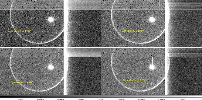
Figure 22: This shows the deviation of electron paths near the edge of the chip due to the lateral electric fields.
Diffusion is off for this plot
Figure 23: This shows the measured and simulated astrometric shifts at the array edge, with several parameters
varied. The simulation captures the major trends of all of these variables. The simulation was not run for Vbb=0,
where the chip is not fully depleted.
263.5 Output transistor characteristics
This section shows simulations that were done to model the output transistor of the ITL STA3800C. Figure 24
shows the simulated and measured Id − Vg characteristics. We obtained a relatively good fit of the transistor
turn-on. This simulation is run with the “trans.cfg” example at [2].
1.0 STA3800C Id-Vg
Measured
0.8
Sim - Qss = 1.1e+12
0.6
Ids(mA)
0.4
Vds = 0.5V
0.2
0.0
25 20 15 10 5 0 5 10 15
Vgs (volts)
(a) Photograph of the (b) Simulation of the same region (c) Simulated and measured I-V
output circuitry
Figure 24: Simulation of the ITL STA3800C output transistor I-V characteristics, compared to measurements.
3.6 Other qualitative tests
Some other tests have been run which have given results which are qualitatively reasonable, but which have not
been compared with quantitative measurements, and three of these are reviewed here. The first of these are known
as “tree rings”. As is well known, periodic dopant variations introduced during the growth of the silicon boule can
lead to measurable variations in flat fields, as well as introducing astrometric pixel shifts (see, for example, [10]).
This effect has been successfully simulated, as shown in Figure 25. This simulation is run with the “treering.cfg”
example at [2].
27Tree Rings: Amplitude = 0.10, Angle = 38.00 degrees, Period = 46.00 microns
Background Doping (cm−3 )
300 Pixel Displacement
350
250 0.10 Pixel
300
200 250
150 200
150
100
100
100 150 200 250 300
50
50 100 150 200 250 300 350
1.2 1.1 1.0 0.9 0.8
1e12
Tree Rings: Amplitude = 0.03, Angle = 38.00 degrees, Period = 46.00 microns
(a) Simulated tree rings with 10% dopant variation
Background Doping (cm−3 )
300 Pixel Displacement
350
250 0.10 Pixel
300
200 250
150 200
150
100
100
100 150 200 250 300
50
50 100 150 200 250 300 350
1.2 1.1 1.0 0.9 0.8
1e12
(b) Simulated tree rings with 3% dopant variation
Figure 25: Simulations of “tree rings”. A sinusoidal dopant variation in the silicon bulk is introduced, varying in
X and Y, and constant in Z. The resulting astrometric pixel shifts are characterized. The X and Y axes are in
pixels. The lower value is more consistent with actual observations.
A second interesting simulation is of the backside substrate connection VBB . It is often questioned how this
bias voltage, which is only connected to the CCD frontside, is conducted to the backside when the CCD is fully
depleted. The answer is that there is an undepleted region near the chip edge which serves this purpose. It is
interesting to simulate this connection, and the result is shown in Figure 26.
28(a) TSi = 100µm; VBB = −60V (b) TSi = 200µm; VBB = −9V
Figure 26: Simulations of the VBB guard rings for two different conditions. In both cases, the top of the simulation
region is where photons are incident, and the left-hand edge is the edge of the CCD. The imaging region begins
at the right-hand edge of the simulation region and continues to the right. The colors are the log of the hole
concentration (in code units), as shown in the colorbar. The imaging region in the left-hand simulation is fully
depleted, while in the right-hand one, which is thicker and has a lower bias voltage, it is not.
While the simulator solves for the condition of the CCD in equilibrium, and does not do transient simulations,
it is possible to simulate transient effects by repeatedly solving for the state of the CCD with small incremental
changes to the boundary conditions. These can then be stitched together to form a movie of the results. An
example of the parallel charge transport is shown in Figure 27. Several movies constructed in this way are
available at [2].
29You can also read