Reversible tuning the optical properties of defective TMDs monolayers
←
→
Page content transcription
If your browser does not render page correctly, please read the page content below
physica status solidi

                                                   Reversible tuning the optical
                                                   properties of defective TMDs
                                                   monolayers
                                                   Mohammad Bahmani*,1 , Michael Lorke*,1,2 , Mahdi Faghihnasiri3 , Thomas Frauenheim*,1,4,5
                                                   1
                                                     Bremen Center for Computational Materials Science, Department of Physics, Bremen University, Am Fallturm 1, 28359 Bremen,
                                                   Germany
arXiv:2010.01115v3 [physics.comp-ph] 11 Sep 2021

                                                   2
                                                     Institute for Theoretical Physics, Department of Physics, Bremen University, Otto-Hahn Alle, 28334 Bremen, Germany
                                                   3
                                                     Computational Materials Science Laboratory, Nano Research and Training Center, 1478934371 Tehran, Iran
                                                   4
                                                     Beijing Computational Science Research Center (CSRC), 100193 Beijing, China
                                                   5
                                                     Shenzhen JL Computational Science and Applied Research Institute, 518110 Shenzhen, China

                                                   Key words: two-dimensional materials, TMDs, strain engineering, optical spectra, simple vacancies and vacancy complexes
                                                   ∗
                                                       Corresponding author: mbahmani@uni-bremen.de, mlorke@itp.uni-bremen.de, frauenheim@bccms.uni-bremen.de

                                                       Potential applications of monolayer of transition metal dichalcogenides (TMDs) in optoelectronic and flexible
                                                       devices are under heavy investigation. Although TMDs monolayers are highly robust to external mechanical
                                                       fields, their electronic structure is sensitive to compressive and tensile strain. Besides, intrinsic point defects are
                                                       present in synthesized samples of these two dimensional (2D) materials which leads to the modification of their
                                                       electronic and optical properties. Presence of vacancy complexes leads to absorption with larger dipole matrix
                                                       elements in comparison to the case of simple transition metal vacancies. Using first principles calculations, we
                                                       scrutinize the effect of various strain situations on the absorption spectra of such defective monolayers and
                                                       show that strain engineering allows for reversible tuning of the optical properties.

                                                                                                                                                    Copyright line will be provided by the publisher

                                                       1 Introduction The semiconducting molybdenum (M o)            These midgap states lead to new optical transitions in
                                                   and tungsten (W ) dichalcogenide monolayers (ML), with            the spectra, making the defective TMDs monolayers even
                                                   direct bandgap, high carrier mobility, and unique opti-           more interesting for electronic and optoelectronic devices
                                                   cal and mechanical properties, are widely investigated as         [21, 3, 9, 11]. Particularly, defect luminescence centers are
                                                   they have shown promising applications in electronics             promising candidates for light-emitting diodes (LEDs)
                                                   and optoelectronics [1–4]. Such 2D TMDs exhibit supe-             and lasers [22–24, 11]. In addition, single-photon emission
                                                   rior photoluminescence (PL) in the visible range [5, 1].          from defect levels (DLs) inside the bandgap of monolay-
                                                   It has been observed that in all the synthetic samples of         ers of molybdenum disulfide (MoS2 ) and tungsten dis-
                                                   MLs TMDs, produced via the chemical vapor deposition              elenide (WSe2 ) were observed [25–27, 11]. It has been
                                                   and the mechanical exfoliation, structural imperfections          measured that photo-excited charge carriers can be trapped
                                                   are always present, in particular point vacancies [6–9]. At       at the midgap localized levels, which, in turn, leads to
                                                   post growth phase, processes like vacuum annealing, ion           a growth of the photocurrent in photodetectors based on
                                                   bombardment, chemical treatment, or ion irradiation, can          MLs MoS2 [28–30]. Hence, scrutinizing the optical prop-
                                                   also be used to introduce such defects onto the monolyers         erties of crystalline point defects inside MLs TMDs is of
                                                   [10–12]. As a consequence, the defect engineering has             great importance both from the application and the funda-
                                                   been proposed to tune the electronic and optical properties       mental point of view [9, 3, 5, 4].
                                                   of 2D TMDs [13–17]. Among these defects, vacancies                    Experimental measurements have shown that MLs TMDs
                                                   induce localized defect states deep inside the band gap           are highly stable under external mechanical fields com-
                                                   and close to the valance band maximum (VBM) as well               pared to conventional bulk semiconductors [31–34]. At the
                                                   as the conduction band minimum (CBM) [7, 18, 8, 19, 20].          same time, the electronic and optical properties of such

                                                                                                                                                    Copyright line will be provided by the publisher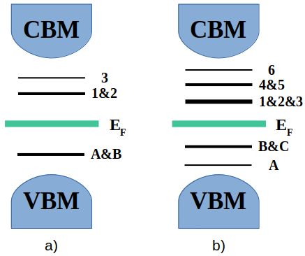
2                                                                                                                             :

2D materials are proven to be sensitive to compressive and       bandgap, in particular for the case of TMDs monolayers.
tensile strain [15, 16, 35, 34, 36]. For example, it was shown   However, previous studies have shown that using more
that MLs TMDs undergo a direct-indirect bandgap transi-          sophisticated methods would only lead to similar relative
tion via applying 1.5% uniaxial strain [16, 15]. As a large      shifts in the band edges and DLs, but do not change the
biaxial strain is applied to MoS2 monolayer, its bandgap         qualitative picture of the defect states within the bandgap
can be reversibly and continuously tuned up to 500 meV           [49–51]. Within the Troullier-Martin approach, we have
[34]. These unique features establish their great advan-         generated a norm-conserving and relativistic pseudopo-
tages over conventional semiconductors for applications in       tentials, including core electrons, to describe the valance
transparent and flexible electronic and optoelectronic de-       electrons [43, 44]. Values for the Energy-Shift and the
vices [2, 37, 23, 4]. Integrating onto microelectromechani-      SplitNorm are equal to 0.02Ry and 0.16, respectively. Lat-
cal systems (MEMS), strain of more than 1.3% has been            tice vectors and atomic positions of the equilibrium and
applied to MLs MoS2 , which lays the ground for novel            strained configurations are optimized using the conjugate-
applications of 2D TMDs in flexible LEDs and field-effect        gradient (CG) method. The lower limit for the Hellmann-
transistors (FETs) [38]. Biaxial strain has been observed        Feynman forces on each atom is set to 0.01 eV /Å. In order
to tune the characteristics of photodetector devices based       to minimize spurious defect-defect interactions between
on MLs MoS2 [39]. Recently, we showed the possibility            the defect images in adjacent supercells as much as possi-
to engineer the degenerate DLs of sulfur and molybde-            ble, we calculate the properties of defective MoS2 (WSe2 )
num vacancies inside MLs MoS2 via various mechanical             monolayers for supercell sizes of 6×6×1 to 9×9×1. Our
deformations [20]. Here, the C3v symmetry of the hexag-          intention is to investigate the properties of isolated defects,
onal monolayers were broken by the applied strain, thus,         rather than the influence of defect concentration. Accord-
splitting the degenerate DLs inside the bandgap up to 450        ingly, we found that for practical calculations, monolayers
meV.                                                             of 8×8×1 are a good compromise between accuracy and
    In this paper, we study the effect of three different        numerical efforts, for transition metal vacancies as well
compressive and tensile strain on the optical properties of      as for vacancy complexes. On the other hand, this super-
MoS2 and WSe2 monolayers, containing transition metal            cell sizes are too small to observe ripple structures due
vacancies and vacancy complexes. Using density func-             to compressive strain. Normal to the layers, a vacuum of
tional theory (DFT), we analyze the change in absorption         40 Å is considered to avoid interactions between adja-
spectra of such defective monolayers within the linear re-       cent monolayers. The convergency of the total energy is
sponse regime. At zero strain, the optical response from         ensured as the difference between two consecutive self-
defects inside MLs MoS2 are different than vacancies             consistent field steps is set to less than 10−4 eV . The Bril-
inside MLs WSe2 . Applying various mechanical defor-             louin zone of supercells is sampled by a 5×5×1 k-points
mations to MLs TMDs modifies the absorption strength,            in the Monkhorst-Pack scheme to obtain both geometries
depending on the type of vacancy. Several defect-defect          and electronic properties. The Hartree, exchange, and cor-
transitions (DDTs) become visible if strain is applied to        relation contribution to the total energy in the real space
the defective monolayers.                                        are calculated using a mesh cut-off of 450 Ry. The energy
                                                                 cut-off and k-points are considered converged when total
    The paper is organized as follows: In section 2, we ex-
                                                                 energy differences were below 10−4 eV and 10−5 eV ,
plain the details of the computations method. In section 3,
                                                                 respectively. According to previous theoretical studies, the
the main results of the paper are shown. We conclude with
                                                                 ground state of defective MLs TMDs is non-magnetic up
a summary and discussion in section 4.
                                                                 to more than 5% strain [45–48]. Since we only applied
                                                                 2% of mechanical deformations to the monolayers, spin-
    2 Computational Details Semiconducting TMDs                  polarization is not considered in this paper. The qualitative
monolayers, with hexagonal symmetry, are constructed of          picture of the electronic structure of TMDs monolayers
a triple X-M-X layer, where the transition metal M is co-        containing point defects is preserved in the presence of
valently bonded to two chalcogen atoms X [2, 16, 9]. In the      the spin-orbit coupling (SOC), even though SOC splits the
present work, we focus on two polytypes: MoS2 and WSe2 ,         VBM [49–51]. Due to the fact that it has minor influence
which are also the experimentally most investigated ones.        on the provided analysis and the final conclusions, SOC is
First-principles calculations are performed using the DFT        neglected in the present work.
formalism as implemented in the SIESTA code [40, 41].
The wavefunction for the valance electrons are expanded              Fig. 1 shows the position of the point vacancies and
by a linear combination of double-zeta basis sets with po-       their neighboring atoms inside MLs MoS2 (MLs WSe2 ).
larization function (DZP). The 4p diffusive orbitals are also    In this paper, we study MoS2 and WSe2 monolayers with
included to improve the characterization of sulfur atoms.        a transition metal vacancy VM and vacancy complexes
The exchange and correlation interactions are described          VM +3X , where M is M o,W , and X is S, Se. There are
using the generalized gradient approximation (GGA) via           computational studies in addition to experimental obser-
the semilocal XC-functional of Perdew-Burke-Ernzerhof            vation of such vacancies in MLs TMDs samples [7–9, 52,
(PBE) [42]. The GGA-PBE functional underestimates the            53]. It is as well possible to introduce these vacancies by

Copyright line will be provided by the publisher
pss header will be provided by the publisher 3
energy bands with k-vector k. Parameter m is the electron
mass, ~ω is the photon energy, and pc,v is the momen-
tum operator. An optical mesh size and broadening of
25×25×1 and 0.02 eV are chosen, respectively.
We focus here on the dipole transition strength of var-
ious inter DL transitions under the influence of differ-
ent types of strain. Although including the many-body ef-
fects modify the electronic and optical properties of TMDs
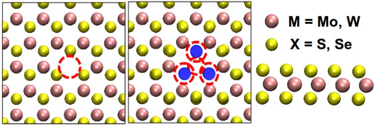
Figure 1 (Color online) Left) A monolayer of MoS2 (WSe2 ) monolayers, there are strong experimental evidence, as
containing the point defects: VM and VM +3X . In every calcula- in Refs. [10, 11, 56, 57], of peaks at energies below the
tion, we only focus on one of these vacancies inside the mono- bandgap. These peaks were identified to be correspond-
layers. Red dashed-circles denote the position of the missing ing to DDTs. Considering such effects into the calculations
metal or chalcogens inside the monolayers. Right) side-view of
does not change the characteristics of optically active and
MLs TMDs. Here, M = M o, W , and X = S, Se.
inactive states. Besides, in order to avoid defect-defect in-
teractions, we study a very large system size, for which it
is prohibitive to include a description of the level of many-
plasma exposure and ion-irradiation [12, 11, 53]. For both body perturbation theory (like a GW0+BSE approach).
defect cases, the C3v symmetry of hexagonal structures are Thus, we have neglected the electron-hole Coulomb inter-
preserved, as shown in Fig. 1. The atomic geometries are actions in this work. As we consider only linear optical
depicted via the VMD tool [54]. absorption and hence probing the states which would be
We examine the effect of three different compressive available for excitation, geometry relaxation via the exci-
and tensile strain on the optical properties of defective tation process does not play a role here, in contrast to stud-
MoS2 (WSe2 ) monolayers, which are shown in Fig. 2. For ies based on photoluminescence, where actual electrons are
the purpose of resembling simple deformations, we con- excited.
sider uniaxial strain in X- and Y-direction. There is also an
inhomogeneous shear type strain (shear T1) which main- 3 Results and Discussion We investigate the ef-
tains the magnitude of in-plane lattice vectors but changes fect of various strain situations on the optical properties of
the angle between them. These types of strain are calcu- MoS2 and WSe2 monolayers containing transition metal
lated at 2% of compression and 2% of stretching, yet they vacancies, VM , as well as vacancy complexes, VM +3X .
are below the breaking point of the monolayers [31]. For this purpose, the optical spectra are investigated via
the imaginary part of the dielectric function, Im[ε]. The
presence of such vacancies in the synthesized samples
have been observed in atomic-resolution measurements
and studied via theoretical methods [7, 8, 52, 53]. More-
over, these defects can also be introduced to the TMDs
monolayers by post processing techniques, such as plasma
exposure and ion-irradiation [12, 11, 53].
3.1 Electronic structure A schematic of the elec-
tronic structure of these defective monolayers is displayed
in Fig. 3. Here, we show the VBM, the CBM, and the
Fermi energy (EF ) as well as the DLs. The occupied DLs
Figure 2 (Color online) schematic view of the uniaxial strain in are named with letters A to C, while the unoccupied DLs
a) X-direction, and b) Y-direction, c) sheer T1 strain.
are labeled with numbers 1 to 6. Based on first-principles
DFT analysis, there are five DLs in the band structure of
Optical properties are calculated using the SIESTA MoS2 (WSe2 ) monolayers with a single transition metal
code, in which, the linear response function is used to com- vacancy, VM o (VW ), as shown in Fig. 3a. Two occupied
pute the imaginary part of the dielectric function Im[ε(ω)] double-degenerate levels are labeled A&B, while 1&2 are
[55]: the double-degenerate unoccupied DLs and 3 is a non-
2 degenerate state. Structures with vacancy complexes of
1 2πe X
Im[ε(ω)] = |pc,v |2 VM o+3S and VW +3Se are shown in Fig. 1. Figure 3b
4πε0 mω shows a schematic of their electronic structure; B&C are
k
(1)
× δ(Ec (k) − Ev (k) − ~ω) double-degenerate occupied DLs. There are also six un-
occupied localized states, a triple-degenerate 1&2&3, a
× [f (Ev (k)) − f (Ec (k))] .
double-degenerate 4&5, and a non-degenerate level 6.
Here, c and v subscripts are denoting conduction and These results are in accordance with previous reports [7, 8,
valance bands properties, respectively. Ec,v (k) are the 18–20].
Copyright line will be provided by the publisher4 :
of 4dz2 ,4dXY and 3p orbitals. Hence, corresponding el-
ements of the dipole matrix have zero value, leading to
optically inactive DDTs in the in-plane spectra (See black
curves in Fig. 4). Two peaks with the lowest energy arise
due to the transition between the VBM and unoccupied
double-degenerate DLs. In the inset of Fig. 4, the out-of-
plane absorption spectra (Im[ε⊥ (ω)]) is plotted for un-
strained defective monolayers. In contrast to the case of
in-plane spectra, DDTs A1&2 and B1&2 are visible here.
These states are mainly composed of surrounding atomic
orbitals with components outside of the XY-plane. Fig. 4
also shows the effect of various strain situations on the
spectra of VM o in MLs MoS2 , where DDTs are indicated
with shaded colors. As uniaxial and inhomogeneous shear
T1 strain are applied, transitions between occupied and un-
Figure 3 (Color online) Schematic of the electronic structure of occupied DLs become optically active, due to the change
the defective MLs MoS2 (MLs WSe2 ) with a) VM o (VW ), b) in the hybridization of orbitals surrounding the vacancy.
VM o+3S (VW +3Se ). Valance and conduction band edges, VBM This stems from breaking the hexagonal symmetry of the
and CBM, are shown along with the Fermi energy (EF ). Occu- defective MLs MoS2 via strain, thus removing the degen-
pied (unoccupied) DLs in the bandgap are labeled with letters eracy of the localized states [60, 61, 20]. It can also be
(numbers). A&B, B&C, 1&2, 4&5 are double-degenerate states. explained via the modification of the geometry as function
1&2&3 are triple-degenerate DLs. of applied strain, which is elaborated on in the Appendix.
In the case of 2% stretching in X-direction, three peaks
can be observed corresponding to DDTs B1&2, A1&2,
and B3. Orbital characteristics of occupied level A (B) is
Accordingly, DDTs are indicated corresponding to the modified and now containing a mixture of 4dxy and 3p
levels involved in the transitions: A1,A2,. . . ,B1,. . . ,C6. (4dx2 −y2 ,4dz2 and 3p) orbitals. The first two unoccupied
The orbital characteristics of the localized states and VBM DLs remain intact under this strain, however, the third
are scrutinized to identify the DDTs in the absorption unoccupied localized state is now mainly constructed of
spectra of such monolayers. Major contributions are orig- 4dz2 ,4dXY and 3p orbitals. Modifications of the electronic
inated from the d orbitals of transition metals (M o, W ) structure under 2% of compressive strain leads to observa-
and p orbitals of chalcogens (S, Se). In the case of sim- tion of B1 transition, where both states are originated from
ple metal vacancy in MLs MoS2 , VBM is built from a combination of 4dz2 ,4dXY and 3p orbitals. When uniax-
4dxy ,4dx2 −y2 (4dXY ) and 3px ,3py orbitals, while a mix- ial compressive or tensile strain in Y-direction is applied,
ture of 4dz2 ,4dXY and 3pz orbitals are mainly involved in B3 transition becomes visible in the in-plane response of
the VBM of system with VM o+3S . For VW in MLs WSe2 , the dielectric function, where mostly 4dz2 ,4dXY and 3p
5dz2 and 5dxy ,5dx2 −y2 (5dXY ) orbitals are hybridized orbitals are contributing to both DLs. In general, the ab-
with 4px ,4py ,4pz (4p) orbitals to construct the VBM; sorption strength of DDTs is larger for uniaxial tensile
however, only 5dz2 ,5dXY orbitals contribute to the VBM than compressive strain. The influence of compressive and
when VW +3Se is present in monolayers. These findings tensile shear T1 strain on the optical response of MoS2
are in line with previous studies [58, 59, 19]. Orbital char- monolayers with VM o are similar and lead to a peak stem-
acteristics of the DLs for each vacancy are presented in ming from B1 transition. Here, 4dz2 ,4dXY and 3p orbitals
corresponding sections. are mainly contributing to these states.
3.2 Optical properties We investigate the effect of
various types of strain on the absorption spectra of these The presence of a simple metal vacancy, VW , in
defective monolayers within the linear response regime. MLs WSe2 results in localized states inside the bandgap.
Peaks at energies below the bandgap indicate the presence In Fig. 5, the optical spectra are shown (black lines) for the
of optically active DLs within the electronic structure of unstrained defective structure. Two peaks corresponding
defective monolayers. to transitions A1&2,B1&2 and A3,B3 are highlighted. The
Simple transition metal vacancy The optical prop- fact that DDTs are visible in the spectra is in explicit con-
erties of MLs MoS2 with VM o vacancy are shown in Fig. 4. trast to the case of M o vacancy in MLs MoS2 at zero strain.
We study the in-plane imaginary part of the dielectric func- This translates into differences in orbital characteristics of
tion (Im[εk (ω)]) for the unstrained case (black lines) and the DLs in two materials. For the case of VW in MLs WSe2 ,
under various types of compressive (blue lines) and tensile two occupied localized states A and B are constructed of
(red lines) strain. Orbitals 4dxz ,4dyz and 3px ,3py ,3pz (3p) 5d orbitals mixing with 4p orbitals, and three unoccu-
are main components of two occupied states A and B, pied DLs have major contributions from 5dz2 ,5dXY and
while unoccupied DLs are constructed from a mixture 4p orbitals. On the other hand, localized states in un-
Copyright line will be provided by the publisherpss header will be provided by the publisher 5
Figure 4 (Color online) The absorption spectra for MLs MoS2 with VM o at zero strain (black lines) and under 2% compressive (blue
lines) and 2% tensile (red lines) strain. The inset is the out-of-plane response of the defective monolayer. From left to right, the plots
represent the effect of strain in X-direction, Y-direction, and shear T1 strain. For each strain case, DDTs are labeled and highlighted
with shaded colors.
Figure 5 (Color online) The absorption spectra for MLs WSe2 with VW at zero strain (black lines) and under 2% compressive (blue
lines) and 2% tensile (red lines) strain. From left to right, the plots represent the effect of strain in X-direction, Y-direction, and shear
T1 strain. For each strain case, DDTs are labeled and highlighted with shaded colors.
Copyright line will be provided by the publisher6 :
strained MLs MoS2 with VM o are mainly constructed are mainly composed of 4d and 3p orbitals. Even though
from 4dxz ,4dyz and 3p orbitals. Comparing Figs. 4 and 5, the degeneracy of DLs is broken via applying uniaxial and
it can be seen that dipole matrix elements are larger for VW inhomogeneous strain, orbital contributions to the local-
than VM o . In Fig. 5, the effect of various strain situations ized states remain untouched. Except for the case of tensile
on the absorption spectra of these defective WSe2 mono- strain in X- and Y-direction, where the occupied state A
layers are displayed where DDTs are labeled and shown is mostly constructed from a mixture of 4d and 3py ,3pz
with shaded colors. In the case of 2% uniaxial tensile orbitals. As monolayers are stretched or compressed by
strain in X-direction, although the orbital characteristics 2% of uniaxial strain, four optically active DDTs can be
of the unoccupied states remain unchanged, states A and seen in the spectra. These are indicated in Fig. 6 with their
B are now dominated with 5dxz ,5dxy ,5dyz ,5dz2 ,4p and corresponding labels. Applying 2% of either compressive
5dz2 ,5dXY ,4p orbitals, respectively. Peaks corresponding or tensile shear T1 strain leads to identical modifications
to DDTs A1&2 and B3 are visible. Applying 2% of com- in the optical spectra, i.e. four peaks corresponding to
pressive strain in X-direction, three transitions B1, A1, and transitions C1, B1,C2&3, C4, and A2&3,B4,C5 can be
B3 can be observed. Here, there are modifications only observed. All being said, the absorption strength of DDTs,
in the major orbitals contributing to the states A and B consequently their brightness, is reduced by a factor of
as well as the first unoccupied level. When uniaxial strain almost two (three) via uniaxial (inhomogeneous shear T1)
in Y-direction are applied, hybridization of the occupied strain.
DLs A and B are changed, while the main orbital compo-
nents of the unoccupied states stay unaffected. Thus, the
degeneracy breaking leads to the observation of A1–3 and
B1–3 transitions in the spectra. When 2% compressive or The absorption spectra of unstrained MLs WSe2 with
tensile shear T1 strain is applied to MLs WSe2 with VW , the vacancy complex VW +3Se is shown with black curves
orbitals 5dz2 ,5dXY and 4p have the largest coefficients in Fig. 7. Two sets of optically active DDTs can be seen, i.e.
in wavefunction expansion of states A and B. The first B1&2&3,C1&2&3 and A1&2&3. It should be noted that
unoccupied DL is now constructed of 5d and 4p orbitals. B&C are double-degenerate occupied states, and 1&2&3
Peaks corresponding to DDTs B1, B2, and B3 are shown are triple-degenerate unoccupied levels. Interestingly, the
in Fig. 5. dipole matrix elements of the first peak is about five times
larger than the intensity of the peaks in the optical response
Vacancy complexes In synthesized samples as well as of MLs WSe2 with VW (See Fig. 5). This outcome em-
during post processing mechanisms, vacancy complexes, phasizes our hypothesis that in ion-irradiated samples, the
i.e. VM o+3S and VW +3Se , are more likely to be present main source of single-photon emissions could be vacancy
than single transition metal vacancies, according to previ- complexes rather than single transition metal vacancies. At
ous studies [8, 59, 61, 60, 20]. This is particularly important zero strain, 5d orbitals of W have the largest coefficients in
when generating vacancies for single-photon emitters at wavefunction expansion of state A, which stays untouched
selective sites [12, 11]. We investigate the optical proper- as all strain situations are applied. Orbital characteristics
ties of MoS2 and WSe2 monolayers containing vacancy of the occupied DLs B and C are mainly a combination
complexes at zero strain and under various mechanical of 5d and 4p orbitals. In the case of the unstrained de-
deformations. Such studies are also of interest for the fective monolayers, major contributions to all unoccupied
production of flexible optoelectronic devices. In compar- DLs come from 5d and 4p orbitals which remain the same
ison to the case of VM o (VW ) vacancies in MLs MoS2 under any types of strain. In Fig. 7, blue (red) lines show
(MLs WSe2 ), out-of-plane optical responses are negligi- the impact of various compressive (tensile) strain on the
ble for monolayers with the complex vacancies, VM o+3S optical spectra of the defective monolayers, where DDTs
(VW +3Se ). are indicated with shaded colors and corresponding labels.
Shown in Fig. 6, the in-plane imaginary part of the When 2% of compression or tensile uniaxial strain is ap-
dielectric function is plotted for MoS2 monolayers with plied to the defective MLs WSe2 , degeneracy of the occu-
VM o+3S . In this figure, optically active DDTs are high- pied DLs B and C is removed due to changes in their orbital
lighted. Their dipole matrix elements are noticeably much characteristics. This leads to the observation of several op-
larger than peaks in the absorption spectra of MLs MoS2 tically active DDTs in the spectra, as indicated in Fig. 7.
with VM o (See Fig. 4). This could be an evidence that in Shear T1 compressive and tensile strain result in analogous
ion-irradiation processes, single photons are emitted from modifications to the absorption spectra of MLs WSe2 with
vacancy complexes rather than simple transition metal VW +3Se . Three peaks corresponding to DDTs C1, B1 and
vacancies. The peak with the highest absorption comes A1,C3 can be seen in the spectra. Here, only the orbital
from DDTs B1&2&3, and C1&2&3, i.e. transitions from components of the occupied state B is changed to a mixture
double-degenerate DLs B&C to triple-degenerate unoccu- of 5d and 4px ,4py orbitals. It can be observed in Fig. 7 that
pied localized states 1&2&3. The other peak is originated the absorption strength are decreased by a factor of almost
from transitions A1&2&3, B4&5, and C4&5. Unoccupied three as uniaxial or inhomogeneous strain are applied, for
DLs 4&5 are double-degenerate. At zero strain, all the DLs both compressing and stretching.
Copyright line will be provided by the publisherpss header will be provided by the publisher 7
Figure 6 (Color online) The absorption spectra for MLs MoS2 with VM o+3S at zero strain (black lines) and under 2% compressive
(blue lines) and 2% tensile (red lines) strain. From left to right, the plots represent the effect of strain in X-direction, Y-direction, and
shear T1 strain. For each strain case, DDTs are highlighted with shaded colors and their labels.
Figure 7 (Color online) The absorption spectra for MLs WSe2 with VW +3Se at zero strain (black lines) and under 2% compressive
(blue lines) and 2% tensile (red lines) strain. From left to right, the plots represent the effect of strain in X-direction, Y-direction, and
shear T1 strain. For each strain case, DDTs are highlighted with shaded colors and their labels.
Copyright line will be provided by the publisher8 :
4 Conclusion In this paper, we have investigated the [10] J. Klein, A. Kuc, A. Nolinder, M. Altzschner,
optical properties of MLs MoS2 and MLs WSe2 containing J. Wierzbowski, F. Sigger, F. Kreupl, J. J. Finley,
point vacancies; VM and VM +3X . The optical spectra are U. Wurstbauer, A. W. Holleitner, and M. Kaniber, 2D
calculated using DFT. At zero strain, it is shown that DDTs Materials 5(1), 011007 (2018).
are visible in the in-plane spectra for VW in MLs WSe2 in [11] J. Klein, M. Lorke, M. Florian, F. Sigger, L. Sigl, S. Rey,
contrast to MLs MoS2 with VM o . According to our study, J. Wierzbowski, J. Cerne, K. Müller, E. Mitterreiter,
dipole matrix elements of peaks originated from DDTs are P. Zimmermann, T. Taniguchi, K. Watanabe, U. Wurst-
significantly larger for the case of the vacancy complexes bauer, M. Kaniber, M. Knap, R. Schmidt, J. J. Finley,
than the simple vacancies. and A. W. Holleitner, Nature Communications 10(1), 2755
The effect of two uniaxial and an inhomogeneous shear (2019).
[12] M. Ghorbani-Asl, S. Kretschmer, D. E. Spearot, and A. V.
T1 strain on the optical properties of defective TMDs
Krasheninnikov, 2D Materials 4(2), 025078 (2017).
monolayers is studied. Interestingly, DDTs in MLs MoS2
[13] A. M. Van Der Zande, P. Y. Huang, D. A. Chenet, T. C.
with VM o become visible in the in-plane spectra as me-
Berkelbach, Y. You, G. H. Lee, T. F. Heinz, D. R. Reich-
chanical deformations are applied. We trace this behavior man, D. A. Muller, and J. C. Hone, Nature Materials 12(6),
back to the change in the hybridization of atomic orbitals 554–561 (2013).
surrounding the vacancy at the defect site. Depending on [14] S. Z. Butler, S. M. Hollen, L. Cao, Y. Cui, J. A. Gupta,
the type of strain, the absorption strength of MLs TMDs H. R. Gutiérrez, T. F. Heinz, S. S. Hong, J. Huang, A. F.
with vacancy complexes has been reduced by a factor of Ismach, E. Johnston-Halperin, M. Kuno, V. V. Plashnitsa,
two to three. Thus, the brightness of the spectra from sam- R. D. Robinson, R. S. Ruoff, S. Salahuddin, J. Shan, L. Shi,
ples with point vacancies could be reduced via strain. Ap- M. G. Spencer, M. Terrones, W. Windl, and J. E. Gold-
plying strain allows to tune the optical properties of mono- berger, ACS Nano 7(4), 2898–2926 (2013).
layers in a controllable way. Our findings will be beneficial [15] M. Ghorbani-Asl, S. Borini, A. Kuc, and T. Heine, Physical
to the application of MLs MoS2 in optoelectronic, flexible, Review B 87(23), 235434 (2013).
and piezoelectric devices as well as heterostructure setups. [16] R. Roldán, A. Castellanos-Gomez, E. Cappelluti, and
F. Guinea, Strain engineering in semiconducting two-
Acknowledgements We thank the DFG funded research dimensional crystals, aug 2015.
training group ”GRK2247”. M.B. acknowledges the support pro- [17] M. A. Khan, M. Erementchouk, J. Hendrickson, and M. N.
vided by DAAD and the PIP program at Bremen university. M.B. Leuenberger, Physical Review B 95(24), 245435 (2017).
also thanks Dr. Miguel Pruneda for his help to produce well-
[18] S. Haldar, H. Vovusha, M. K. Yadav, O. Eriksson, and
performed pseudopotentials and basis sets.
B. Sanyal, Physical Review B 92(23), 235408 (2015).
[19] M. Pandey, F. A. Rasmussen, K. Kuhar, T. Olsen, K. W.
References
Jacobsen, and K. S. Thygesen, Nano Letters 16(4), 2234–
[1] K. F. Mak, C. Lee, J. Hone, J. Shan, and T. F. Heinz, Phys- 2239 (2016).
ical Review Letters 105(13), 136805 (2010). [20] M. Bahmani, M. Faghihnasiri, M. Lorke, A. B. Kuc,
[2] Q. H. Wang, K. Kalantar-Zadeh, A. Kis, J. N. Coleman, and T. Frauenheim, Physica Status Solidi (B) Basic Re-
and M. S. Strano, Electronics and optoelectronics of two- search(mar), 1900541 (2020).
dimensional transition metal dichalcogenides, nov 2012. [21] S. Yuan, R. Roldán, M. I. Katsnelson, and F. Guinea, Phys-
[3] K. F. Mak and J. Shan, Photonics and optoelectronics of 2D ical Review B - Condensed Matter and Materials Physics
semiconductor transition metal dichalcogenides, 2016. 90(4), 041402 (2014).
[4] Z. Lin, Y. Lei, S. Subramanian, N. Briggs, Y. Wang, C. L. [22] H. Nan, Z. Wang, W. Wang, Z. Liang, Y. Lu, Q. Chen,
Lo, E. Yalon, D. Lloyd, S. Wu, K. Koski, R. Clark, S. Das, D. He, P. Tan, F. Miao, X. Wang, J. Wang, and Z. Ni, ACS
R. M. Wallace, T. Kuech, J. S. Bunch, X. Li, Z. Chen, Nano 8(6), 5738–5745 (2014).
E. Pop, V. H. Crespi, J. A. Robinson, and M. Terrones, APL [23] F. Withers, O. Del Pozo-Zamudio, A. Mishchenko,
Materials 6(8), 080701 (2018). A. P. Rooney, A. Gholinia, K. Watanabe, T. Taniguchi,
[5] U. Wurstbauer, B. Miller, E. Parzinger, and A. W. Holleit- S. J. Haigh, A. K. Geim, A. I. Tartakovskii, and K. S.
ner, Light-matter interaction in transition metal dichalco- Novoselov, Nature Materials 14(3), 301–306 (2015).
genides and their heterostructures, 2017. [24] S. Wu, S. Buckley, J. R. Schaibley, L. Feng, J. Yan, D. G.
[6] H. P. Komsa, S. Kurasch, O. Lehtinen, U. Kaiser, and A. V. Mandrus, F. Hatami, W. Yao, J. Vučković, A. Majumdar,
Krasheninnikov, Physical Review B 88(035301) (2013). and X. Xu, Nature 520(7545), 69–72 (2015).
[7] W. Zhou, X. Zou, S. Najmaei, Z. Liu, Y. Shi, J. Kong, [25] M. Koperski, K. Nogajewski, A. Arora, V. Cherkez, P. Mal-
J. Lou, P. M. Ajayan, B. I. Yakobson, and J. C. Idrobo, let, J. Y. Veuillen, J. Marcus, P. Kossacki, and M. Potemski,
Nano Letters 13(6), 2615–2622 (2013). Nature Nanotechnology 10(6), 503–506 (2015).
[8] H. P. Komsa and A. V. Krasheninnikov, Physical Review B [26] Y. M. He, G. Clark, J. R. Schaibley, Y. He, M. C. Chen, Y. J.
91(125304) (2015). Wei, X. Ding, Q. Zhang, W. Yao, X. Xu, C. Y. Lu, and J. W.
[9] Z. Lin, B. R. Carvalho, E. Kahn, R. Lv, R. Rao, H. Ter- Pan, Nature Nanotechnology 10(6), 497–502 (2015).
rones, M. A. Pimenta, and M. Terrones, Defect engineer- [27] L. N. Tripathi, O. Iff, S. Betzold, Ł. Dusanowski, M. Em-
ing of two-dimensional transition metal dichalcogenides, merling, K. Moon, Y. J. Lee, S. H. Kwon, S. Höfling, and
apr 2016. C. Schneider, ACS Photonics 5(5), 1919–1926 (2018).
Copyright line will be provided by the publisherpss header will be provided by the publisher 9
[28] N. Perea-López, Z. Lin, N. R. Pradhan, A. Iñiguez-Rábago, [51] B. Schuler, D. Y. Qiu, S. Refaely-Abramson, C. Kastl, C. T.
A. L. Elı́as, A. McCreary, J. Lou, P. M. Ajayan, H. Ter- Chen, S. Barja, R. J. Koch, D. F. Ogletree, S. Aloni, A. M.
rones, L. Balicas, and M. Terrones, 2D Materials 1(1), Schwartzberg, J. B. Neaton, S. G. Louie, and A. Weber-
011004 (2014). Bargioni, Physical Review Letters 123(7), 076801 (2019).
[29] I. Amit, T. J. Octon, N. J. Townsend, F. Reale, C. D. Wright, [52] L. Ma, Y. Tan, M. Ghorbani-Asl, R. Boettger,
C. Mattevi, M. F. Craciun, and S. Russo, Advanced Mate- S. Kretschmer, S. Zhou, Z. Huang, A. V. Krashenin-
rials 29(19), 1605598 (2017). nikov, and F. Chen, Nanoscale 9(31), 11027–11034
[30] M. K. Ghimire, H. Ji, H. Z. Gul, H. Yi, J. Jiang, and (2017).
S. C. Lim, ACS Applied Materials and Interfaces 11(10), [53] M. G. Stanford, Y. C. Lin, M. G. Sales, A. N. Hoffman,
10068–10073 (2019). C. T. Nelson, K. Xiao, S. McDonnell, and P. D. Rack, npj
[31] S. Bertolazzi, J. Brivio, and A. Kis, ACS Nano 5(12), 2D Materials and Applications 3(1), 13 (2019).
9703–9709 (2011). [54] W. Humphrey, A. Dalke, and K. Schulten, Journal of
[32] A. Castellanos-Gomez, M. Poot, G. A. Steele, H. S. J. Van Molecular Graphics 14, 33–38 (1996).
Der Zant, N. Agrat, and G. Rubio-Bollinger, Advanced [55] P. Y. Yu, M. Cardona, P. Y. Yu, and M. Cardona, Intro-
Materials 24(6), 772–775 (2012). duction, in: Fundamentals of Semiconductors, (Springer,
[33] A. Castellanos-Gomez, V. Singh, H. S. Van Der Zant, and Berlin, Heidelberg, 2013), pp. 1–11.
G. A. Steele, Mechanics of freely-suspended ultrathin lay- [56] K. Barthelmi, J. Klein, A. Hötger, L. Sigl, F. Sigger,
ered materials, jan 2015. E. Mitterreiter, S. Rey, S. Gyger, M. Lorke, M. Florian,
[34] D. Lloyd, X. Liu, J. W. Christopher, L. Cantley, F. Jahnke, T. Taniguchi, K. Watanabe, V. Zwiller, K. D.
A. Wadehra, B. L. Kim, B. B. Goldberg, A. K. Swan, and Jöns, U. Wurstbauer, C. Kastl, A. Weber-Bargioni, J. J. Fin-
J. S. Bunch, Nano Letters 16(9), 5836–5841 (2016). ley, K. Müller, and A. W. Holleitner, Atomistic defects as
[35] A. Steinhoff, J. H. Kim, F. Jahnke, M. Rösner, D. S. Kim, single-photon emitters in atomically thin MoS2, aug 2020.
C. Lee, G. H. Han, M. S. Jeong, T. O. Wehling, and C. Gies, [57] E. Mitterreiter, B. Schuler, K. Barthelmi, K. Cochrane,
Nano Letters 15(10), 6841–6847 (2015). J. Kiemle, F. Sigger, J. Klein, E. Wong, E. Barnard,
[36] R. Frisenda, M. Drüppel, R. Schmidt, S. Michaelis De Vas- S. Refaely-Abramson, D. Qiu, M. Lorke, F. Jahnke, J. Fin-
concellos, D. Perez De Lara, R. Bratschitsch, M. Rohlfing, ley, T. U. Muenchen, and A. Schwartzberg(nov) (2020).
and A. Castellanos-Gomez, npj 2D Materials and Applica- [58] E. Cappelluti, R. Roldán, J. A. Silva-Guillén, P. Ordejón,
tions 1(10) (2017). and F. Guinea, Physical Review B - Condensed Matter and
[37] O. Lopez-Sanchez, D. Lembke, M. Kayci, A. Radenovic, Materials Physics 88(7), 075409 (2013).
and A. Kis, Nature Nanotechnology 8(7), 497–501 (2013). [59] C. González, B. Biel, and Y. J. Dappe, Nanotechnology
[38] J. W. Christopher, M. Vutukuru, D. Lloyd, J. S. Bunch, 27(10), 105702 (2016).
B. B. Goldberg, D. J. Bishop, and A. K. Swan, Journal of [60] G. H. Ahn, M. Amani, H. Rasool, D. H. Lien, J. P. Mastan-
Microelectromechanical Systems pp. 1–10 (2019). drea, J. W. Ager III, M. Dubey, D. C. Chrzan, A. M. Minor,
[39] P. Gant, P. Huang, D. Pérez de Lara, D. Guo, R. Frisenda, and A. Javey, Nature Communications 8(1), 608 (2017).
and A. Castellanos-Gomez, Materials Today(may) (2019). [61] M. G. Sensoy, D. Vinichenko, W. Chen, C. M. Friend, and
[40] P. Ordejon, E. Artacho, and J. M. Soler, Physical Review B E. Kaxiras, Physical Review B 95 (2017).
53(16), R10441–R10444 (1996).
[41] J. M. Soler, E. Artacho, J. D. Gale, A. Garcı́a, J. Junquera, Appendix In this appendix, we highlight the rela-
P. Ordejón, and D. Sánchez-Portal, Journal of Physics Con- tion between the change in the geometrical and electronic
densed Matter 14(11), 2745–2779 (2002). properties of defective MLs MoS2 and the modification of
[42] J. P. Perdew, K. Burke, and M. Ernzerhof, Physical Review their optical response. In Fig. A.1, the charge density of
Letters 77(18), 3865–3868 (1996). the monolayers with VM o are shown for (a) 0.0% and b)
[43] N. Troullier and J. L. Martins, Physical Review B 43(3), +2.0% strain in X-direction at isovalue of 0.095 e/Å3 .
1993–2006 (1991). Atoms around the vacancy are labeled with A, B, and C.
[44] N. Troullier and J. L. Martins, Physical Review B 43(11), At zero strain, symmetric structure of the monolayer is un-
8861–8869 (1991). touched and the distance between the neighboring atoms is
[45] P. Tao, H. Guo, T. Yang, and Z. Zhang, Journal of Applied 3.238Å for MLs MoS2 with VM o and 3.176Å for pristine
Physics 1151(10), 44311–173105 (2014). geometry. When 2.0% of tensile strain in X-direction is ap-
[46] H. Zheng, B. Yang, D. Wang, R. Han, X. Du, and Y. Yan, plied, the AC and BC distances are 3.262Å and 3.192Å for
Applied Physics Letters 1041(10), 132403–44311 (2014). defective monolayer and pristine structure, respectively.
[47] W. S. Yun and J. D. Lee, Journal of Physical Chemistry C However, since atoms at A and B positions are along the
119(5), 2822–2827 (2015). strain direction, the AB distance for the case Mo vacancy in
[48] A. Li, J. Pan, Z. Yang, L. Zhou, X. Xiong, and F. Ouyang, MLs MoS2 has been increased by 5.8% to 3.426Å, which
Journal of Magnetism and Magnetic Materials 451(apr), is much larger than for pristine structure with the expected
520–525 (2018). 2.0% increase to 3.240Å. This geometry modification is
[49] S. Refaely-Abramson, D. Y. Qiu, S. G. Louie, and J. B.
responsible for the changes in optical properties for such
Neaton, Physical Review Letters 121(16) (2018).
defective monolayers, as shown in Fig. 4.
[50] M. H. Naik and M. Jain, Physical Review Materials 2(8),
084002 (2018).
Copyright line will be provided by the publisher10 : Figure A.1 (Color online) The change in the charge density of the MoS2 monolayers containing VM o under strain in X-direction for an amount of a) 0.0% and b) +2.0%. These are plotted at 0.095 e/Å3 . Atoms around the vacancy are labeled with A, B, and C. Copyright line will be provided by the publisher
You can also read