Spatially controlled nano structuring of silicon with femtosecond vortex pulses - Nature
←
→
Page content transcription
If your browser does not render page correctly, please read the page content below
www.nature.com/scientificreports
OPEN Spatially controlled
nano‑structuring of silicon
with femtosecond vortex pulses
M. G. Rahimian, A. Jain, H. Larocque, P. B. Corkum, E. Karimi & V. R. Bhardwaj*
Engineering material properties is key for development of smart materials and next generation
nanodevices. This requires nanoscale spatial precision and control to fabricate structures/defects.
Lithographic techniques are widely used for nanostructuring in which a geometric pattern on a mask
is transferred to a resist by photons or charged particles and subsequently engraved on the substrate.
However, direct mask-less fabrication has only been possible with electron and ion beams. That is
because light has an inherent disadvantage; the diffraction limit makes it difficult to interact with
matter on dimensions smaller than the wavelength of light. Here we demonstrate spatially controlled
formation of nanocones on a silicon surface with a positional precision of 50 nm using femtosecond
laser ablation comprising a superposition of optical vector vortex and Gaussian beams. Such control
and precision opens new opportunities for nano-printing of materials using techniques such as laser-
induced forward transfer and in general broadens the scope of laser processing of materials.
The fundamental limit to spatial resolution of any optical system is governed by diffraction and is approxi-
mately half the wavelength of l ight1. Diffraction also dictates how tightly a laser beam can be focused, which in
turn determines the feature size one can achieve in laser ablation of materials. Therefore, shorter wavelengths
(ultraviolet) are often used in combination with lithographic techniques to produce sub-wavelength features as
small as 50 nm2. Driven primarily by the semiconductor industry, research efforts are ongoing to use coherent
and non-coherent extreme ultraviolet light to produce features smaller than 10 nm to meet the ever increasing
demand for m iniaturization3,4. Concurrently, alternate methods are also being explored to overcome the dif-
fraction limit of light that does not involve the use of a photomask. These fall into two categories—near field
and far field approaches.
Nanofabrication using near field approach exploits local field enhancement around a nanoparticle to confine
light to sub-wavelength dimensions and thereby induce local deformations (melting or ablation) of the substrate.
Large scale periodic array of nanoholes were fabricated by laser irradiation of a monolayer of microspheres5—a
multistep process with no direct control on the position of nanostructures, analogous to lithographic t echniques6.
Alternately, controlled fabrication of individual nanostructures can be achieved using scanning probe microscope
either directly7 or by irradiating the tip with l ight8.
Direct laser processing of materials is a far field approach that exploits the nonlinear nature of the light-matter
interaction and localized energy deposition. Using ultrashort laser pulses, three-dimensional (3D) control was
achieved in transparent materials9,10 and sub-wavelength structures were created with enhanced spatial precision
in a cold ablation process due to negligible lateral heat transport to the surrounding material. Exploiting near
threshold ablation, feature dimensions far below the diffraction limit were demonstrated11,12. However, in such a
threshold based material response, the ablation features were found not to be dependent on the nonlinear process
responsible for light absorption but rather correspond to a one-to-one mapping of the beam profile at threshold
intensity13. Nanoholes14,15, nanocones16–19, nanodots5 and self-organized periodic nano-ripple patterns20–22 were
also fabricated in different materials either by ablation or material modification using above threshold laser
pulse energies.
Another non-contact direct laser-write technique that is widely used in nano-printing is Laser Induced Fro-
ward Transfer (LIFT) to “drop and place” small volumes of complex materials into user-defined, high-resolution
patterns23,24. A thin film of material on a donor substrate is melted locally by the laser beam and lifted off in the
form of a droplet that gets deposited onto a receiver substrate separated by a small gap. The spatial resolution
one could achieve in placing individual droplets is few hundreds of nanometers.
Department of Physics, University of Ottawa, K1N 6N5 Ottawa, ON, Canada. *email: ravi.bhardwaj@uottawa.ca
Scientific Reports | (2020) 10:12643 | https://doi.org/10.1038/s41598-020-69390-4 1
Vol.:(0123456789)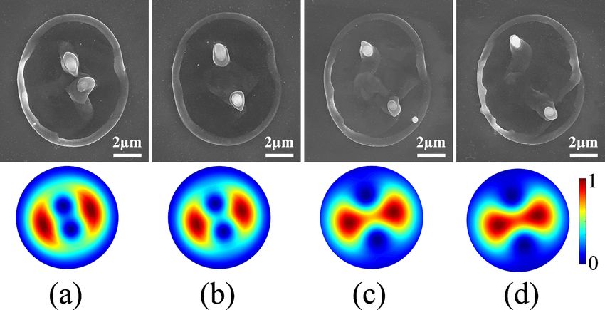
www.nature.com/scientificreports/
Although light induced nanostructures with feature sizes smaller than diffraction limit could be fabricated
either by ablation or material m odification25, the degree of spatial control with light is restrictive. For example,
it is not feasible to position individual structures with nanoscale precision. Only partial spatial control has
been achieved with nano-ripples whose orientation and spacing was varied by changing the laser polarization
and wavelength ( )21. In this context, the present article addresses how light can be used to actively manipulate
materials in two dimensions with a precision of ∼ /20. It demonstrates positioning of ∼ 0.1 µm3 of the molten
material in the form of a nanocone with 50 nm precision in an area of 40 µm2 by manipulating the beam shape.
The technique is extended to fabricate complex, unconventional structures involving multiple nanocones and
control their relative positions with the same precision.
Apart from laser fabrication and spatial control of nanostructures, surpassing the diffraction barrier imposed
by the wave nature of light is also critical in imaging/microscopy. It is accomplished by using the same (a) near
field techniques that exploit the information contained in the evanescent w ave26,27 or confine light using plas-
28,29
monic nanostructures , and (b) far field techniques that exploits the optical nonlinearity of the medium as in
stimulated emission depletion m icroscopy30.
Our approach to sub-wavelength precision in nano-fabrication is based on the coherent superposition of
optical vector vortex beam (VVB) and a Gaussian beam31. VVBs are characterized by spatially variant linear
polarization in the beam transverse plane. They may possess phase singularities in the transverse plane at which
the field amplitude vanishes. VVBs can be expanded in terms of orbital angular momentum (OAM) carrying, i.e.
twisted, beams. Twisted beam carry an OAM value of ℓ per photon, where is the redueced Plank constant, and
ℓ indicates the number of twists in the helical wavefront in one wavelength which its sign determines the chiral-
ity of the helix. We produce VVBs using a birefringent plate enclosing a patterned liquid crystal layer, known
as a q-plate. The liquid crystals in the q-plate have an optic axis whose orientation depends on the azimuthal
coordinate, thereby forming a pattern defined by a topological charge q consisting of either a full or a half-integer
value. As light propagates in the q-plate, spin angular momentum associated with light polarization is coupled
to photon OAM of ℓ = ±2q. The conversion efficiency is determined by the q-plate’s optical retardation, which
can be controlled by an externally applied electric field.
Results
Our technique exploits two unique properties of VVBs. First, the annular intensity distribution of the VVB when
focused is mapped onto the silicon surface causing melting of a thin layer, determined by the optical penetration
depth of light. Thermo-capillary and/or hydrodynamic forces displace the molten silicon radially outward to
the periphery and also radially inward to the centre of the crater. Compressive forces arising from radial inward
motion of the molten material pushes it away from the surface. Rapid expansion causes re-solidification into a
nanocone formed (Fig. 1a) at the centre where VVB has a zero intensity point18. Simultaneously, the radial out-
ward motion of the molten material re-solidifies after reaching the cold boundary of the ablation region to form a
rim. The height of the nanocone is ∼ 500 nm and increases with the increasing pulse energy while the rim height
is only ∼ 100 nm18. Longer nanocones or nanoneedles have been produced with vortex beams using nanosecond
and picosecond pulses on s ilicon32 and m etals33. They were shown to exhibit chirality and has been attributed
to (a) mapping of the orbital angular momemtum of the beam on to the handedness of the n anoneedles33, and/
or (b) tailored chiral intensity distribution that also controls the handedness of n anoneedles34. In contrast, there
was no clear signature of the chirality-control fabrication (by changing OAM value) of nanocones produced by
femtosecond pulses.
Second, when a pure VVB is perturbed by adding coherently a tunable amount of a linearly polarized Gauss-
ian beam, the central singularity either shifts or unfolds into multiple singularities depending on the topological
charge. The shift can be precisely controlled by adjusting the applied external field to the q-plate. This action varies
the optical retardation and thereby detunes the strength of the spin-to-orbital angular momentum coupling of
light. A fraction of the input Gaussian beam co-propagates with a partly converted VVB. As a result, for q=1/2
or ℓ = ±1, the position of the nanocone within the ablation region can be varied with nanometers precision
(Fig. 1b,c). As the weight of the Gaussian beam increases, the position of the singularity shifts towards the outer
region of the ablated region (also see Supplementary Fig. S2). For a pure VVB produced by q=1/2 plate, the output
polarization was radial, azimuthal, or s piral22 when the angle of the incident linear polarization with respect to
the q-plate axis was 0 ◦ , 90◦ , or 45◦ , respectively.
The nanocone position can be controlled by moving the singularity anywhere in the transverse plane of
the beam as shown in Fig. 2, for azimuthally polarized VVB. For a fixed optical retardation (relative weight of
Gaussian beam to VVB), a half-wave plate (HWP) in front of the detuned q-plate rotates the input polarization
with respect to the q-plate axis and changes the angular position of the singularity at the transverse plane rotat-
ing it in a circular arc. Radius of the circular arc depends on the optical retardation. Varying the applied electric
field to the q-plate and rotating the incident linear polarization, the nanocone can be positioned anywhere in
2D space within the interaction region of ∼ 40 µ m2 with a precision of 50 nm. Similar results were obtained for
radial and spiral VVBs.
Figure 3 shows unfolding of the singularity when a pure VVB with a star-shaped polarization p attern22
with ℓ = ±2 (topological charge of q = −1) is perturbed by a Gaussian beam. The perturbation is achieved by
electrically detuning the q-plate. In VVBs, the total field orientation is undefined along the beam axis and this
polarization singularity is typically referred to as a V-point. A small perturbation to pure VVB causes the local
polarization states to acquire a tiny ellipticity. The V-point no longer exists, instead two pairs of C-points appear
where the orientation of the polarization ellipse is undefined. Unfolding of the polarization singularity also
deforms the intensity pattern of the pure VVB giving rise to two null intensity points. The separation between
these points can be controlled by varying the relative weight of Gaussian beam superimposed on the VVB and
Scientific Reports | (2020) 10:12643 | https://doi.org/10.1038/s41598-020-69390-4 2
Vol:.(1234567890)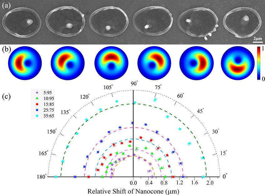
www.nature.com/scientificreports/
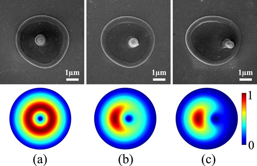
Figure 1. Displacement of the nanocone and phase singularity with retardation. Superposition of linearly
polarized Gaussian beam with VV beam produced by a q-plate with topological charge of q = +1/2, having
different weights (a) 0:100 (pure VV beam), (b) 10:90, and (c) 15:85. The top row shows SEM images of the
nanocone position and the bottom row shows the corresponding intensity profile of the superposition beams.
A single laser pulse with an energy of 280 nJ created the nanocone. The corresponding peak fluence is 2.3 ± 0.3
J/cm2.
increases with the amount of Gaussian contribution. This results in the formation of two nanocones whose
separation and relative orientation can be precisely controlled by detuning the q-plate and adding an extra phase
to the superimposed beams (as in Fig. 2), respectively (see Supplementary Fig. S4).
Figure 4 shows how complex intensity patterns can be generated by superimposing different VVBs produced
by a combination of two q-plates with topological charges of q = −1 and q = 1/2. A HWP between the q = −1
and a detuned q = 1/2 plates produces a superposition state α(ei2φ eR + e−i2φ eL ) + β(eiφ eL + e−iφ eR ), where α
and β are given by the detuning parameter. The resultant intensity distribution displays three singularities around
the central region where the intensity is also minimum (Fig. 4c). As a result 4 nanocones are formed (Fig. 4a).
In the absence of the HWP the output corresponds to a superposition state defined by α(ei2φ eR + e−i2φ eL ) + β
(ei3φ eL + e−i3φ eR ). The intensity pattern consists of 5 null points around the central null region (Fig. 4d). This
should lead to 6 nanocones. However, any slight detuning of the q = −1 plate leads to splitting of the central
singularity resulting in the formation of 7 nanocones (Fig. 4d) (see Supplementary Fig. S6).
Discussion
There are some similarities between our laser processing technique and stimulated emission depletion (STED)
microscopy/ lithography in surpassing the diffraction barrier. Both use superpositions of Gaussian and non-
Gaussian beams. In STED microscopy, a focused Gaussian beam that excites the fluorophores is superimposed
with a beam having a doughnut intensity distribution that switches off the fluorophores except at its centre. In
STED lithography the doughnut beam is used to inhibit photo-polymerization induced by the writing beam.
However, the main drawback of STED lithography is the design and development of suitable p hotoresists35. In
our method, varying the phase retardation between the VVB and Gaussian beam shifts the null intensity posi-
tions within the focal region enabling us to control the position of the nanocone.
However, the underlying physics is different between the two methods. In STED microscopy, the doughnut
beam depletes the fluorescent state by stimulated emission in all molecules in the intense regions of the beam.
The intensity of the doughnut beam determines (a) the probability of fluorescence switching that scales expo-
nentially, and (b) the area to which fluorescence is confined that scales inversely thereby enhancing the spatial
resolution. In our technique, VVB induces localized melting via multiphoton absorption and the subsequent
fluid dynamics around the unmodified region of the material (due to null intensity region) displaces matter on
nanoscale. The probability of such nonlinear interaction scales with nth power of laser intensity, where n is the
number of photons involved in the multiphoton process. In silicon (band gap of 1.14 eV), the interaction of 800
nm light (photon energy of 1.55 eV) is dominated by single and two photon absorption. The intensity of the VVB
Scientific Reports | (2020) 10:12643 | https://doi.org/10.1038/s41598-020-69390-4 3
Vol.:(0123456789)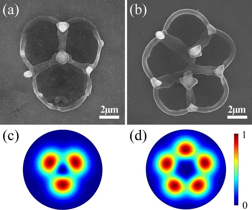
www.nature.com/scientificreports/
Figure 2. Controlled positioning of the nanocone in 2D space. (a) For a fixed relative weight (25:75) of
Gaussian and VV beams produced by an electrically detuned q-plate with topological charge of q=+1/2,
SEM images show the motion of the nanocone in a circular arc when an additional phase is added to the
superimposed beams by rotating the polarization axis of the incident Gaussian beam with respect to the q-plate
axis. A single laser pulse irradiated the sample with a pulse energy of 600 nJ. (b) The corresponding simulated
intensity profiles. (c) Polar plot showing the measured relative shift of the nanocone with respect to its position
for a pure VV beam as a function of the rotation angle of the HWP (relative phase of the linearly polarized
Gaussian beam) for different optical retardations (different weights of Gaussian and VV beams). The dashed
lines are the simulated nanocone position.
determines the amount of the material displaced leading to nanocone formation whose height increases but the
apex angle remains the same18. Therefore, the spatial resolution remains the same.
In our experiments, the spatial precision of ∼ 50 nm is due to loose focusing of the laser beam. The use of
a high numerical aperture lens will reduce the size of the null intensity region and will lead to a smaller lateral
extent and apex angle of the nanocone (see Supplementary Fig. S3). However, at very high numerical apertures
the longitudinal component of the field can hinder the interference process and limit the spatial resolution. The
spatial precision can be further improved to 10 nm by (a) using a highly stable power supply that can change the
small voltage applied to the q-plate in 1 mV steps, and/or (b) changing the angle of the half-wave plate in front
of the detuned q-plate in smaller steps of 0.1◦ . The laser pulse duration is not critical in our technique. In fact,
longer durations were found to give rise to µm sized nano-needles likely due to larger melt v olume19.
The main limitation is that the nanocones can be efficiently created only on non-transparent materials where
the melt layer is two dimensional. In transparent materials, light penetration into the medium leads to a 3D melt
layer whose dynamics lead to surface swelling and ejection of the material instead of a well-defined nanocone.
Also, the nanocones are always accompanied by an outer rim whose relative height can be minimized by laser
parameters albeit with concomitant reduction in nanocone h eight18. Controlled fabrication of nanocones in
semiconductors and metals can be used as field emission tips36,37, scanning probes, whispering gallery optical
resonator38, and for enhanced solar absorption in photovoltaics39. When implemented with LIFT, our technique
provides the ability to control the deposited material with sub-wavelength precision in nano-printing of complex
materials with applications ranging from microelectronics to bio-photonics.
Scientific Reports | (2020) 10:12643 | https://doi.org/10.1038/s41598-020-69390-4 4
Vol:.(1234567890)www.nature.com/scientificreports/
Figure 3. Separation of nanocones with unfolding singularity. Superposition of linearly polarized Gaussian and
VV beams produced by a detuned q-plate, topological charge of q = −1, with different relative weights of (a)
10:90, (b) 15:85, (c) 20:80 (d) 25:75. Top panels shows the SEM images of two nano-cones generated by a single
laser pulse with an energy of 310 nJ. The bottom panels show the corresponding intensity profiles. Separation
between the singularities increases with increase in the Gaussian component.
Figure 4. Fabrication of complex nanostructures. Mapping of complex intensity profiles generated by VVB
produced by two q-plates with topological charge of q = −1, and q = 1/2. (a) A HWP between the q = −1
(ℓ = ±2) plate and a detuned q = 1/2 (ℓ = ±1) plate, and (b) without the HWP between the two q-plates. The
corresponding calculated intensity profiles are shown in (c, d). Experimental patterns were produced by a single
pulse with an energy of 700 nJ.
Methods
Experiment. Femtosecond light pulses from a Ti:sapphire laser system (800 nm, 1 kHz, 45 fs, 2.5 mJ/pulse)
were focused on a silicon surface with a 0.25 NA (16X) aspheric lens. The sample was mounted on three-axis
translation stages with a resolution of 100 nm. The sample was irradiated with a single pulse selected by operat-
ing the laser in an external trigger mode. The incident pulse energies, varied using a half-wave plate (HWP) and
a polarizer, were measured after the microscope objective taking into account the transmission and reflection
Scientific Reports | (2020) 10:12643 | https://doi.org/10.1038/s41598-020-69390-4 5
Vol.:(0123456789)www.nature.com/scientificreports/
losses of all the optics. The pulse duration before the microscope objective was 70 fs. The laser-ablated regions
were characterized by a scanning electron microscope (SEM), with the electron beam incident normal to the
sample surface and atomic force microscopy (AFM) in non-contact mode.
In our experiment, complex intensity profiles were generated using birefringent-based liquid crystal beam
converters, called q-plates40,41, with topological charges of q = +1/2 and −1. The optical retardation of the
q-plates was changed by varying the voltage applied to them. At the optimal voltage, the q-plates converted line-
arly polarized Gaussian beams to optical VVBs composed of OAM states with ℓ = ±1 and ℓ = ±2, respectively42.
Complex spatial intensity profiles were produced by varying the voltage applied on the q-plate. This process called
voltage tuning of the q-plate results in varying the extent of coherent superposition of laser beam components.
In other words, detuning the individual q-plate produced a superposition of partially converted VVBs with the
incident Gaussian beam. A combination of different q-plates resulted in complex intensity profiles due to the
superposition of VVBs. See Supplementary Fig. S1 for additional details.
Numerical. Intensity profiles of different order VVBs and their superposition states were simulated using
the Laguerre Gaussian beam
LG √
|ℓ|
Cℓp −r 2 2r 2 −ikr 2
r 2
U(r, φ, z) = exp Lp
|ℓ|
exp − iℓφ − ikz + i�(z) , (1)
w(z) w(z) w 2 (z) w 2 (z) 2R(z)
where p ≥ 0 is the radial index and ℓ is the azimuthal index. Lpℓ are the generalized Laguerre polynomials and
LG
Cℓp is a normalization constant. R(z) is the radius of curvature of the wavefront, w(z) is the beam width and
�(z) is the Gouy phase. r and z are the radial and axial distances. k is the wave number and eiℓφ is the phase
factor containing the ℓ term.
Received: 17 December 2019; Accepted: 8 July 2020
References
1. Abbe, E. A contribution to the theory of the microscope and the nature of microscopic vision. Proc. Bristol Nat. Soc. 1, 20017261
(1874).
2. Lin, B.-J. Immersion lithography and its impact on semiconductor manufacturing. J. Micro/Nanolithogr. MEMS MOEMS 3, 377–395
(2004).
3. Wagner, C. & Harned, N. Lithography gets extreme. Nat. Photonics 4, 24 (2010).
4. Bakhsi, V. EUV Lithography 2nd edn. (SPIE Press, Bellingham, 2009).
5. Pereira, A. et al. Laser fabricated porous alumina membranes for the preparation of metal nanodot arrays. Small 4, 572 (2008).
6. Ito, T. & Okazaki, S. Pushing the limits of lithography. Nature 406, 1027 (2000).
7. Xie, X. N., Chung, H. J., Sow, C. H. & Wee, A. T. S. Nanoscale materials patterning and engineering by atomic force microscopy
nanolithography. Mater. Sci. Eng. R Rep. 54, 1–48 (2006).
8. Jersch, J. & Dickmann, K. Nanostructure fabrication using laser field enhancement in the near field of a scanning tunneling
microscope tip. Appl. Phys. Lett. 68, 868 (1996).
9. Kawata, S., Sun, H.-B., Tanaka, T. & Takada, K. Finer features for functional microdevices. Nature 412, 697 (2001).
10. Yanik, M. F. et al. Functional regeneration after laser axotomy. Nature 432, 822 (2004).
11. Joglekar, A. P., Liu, H.-H., Meyhöfer, E., Mourou, G. & Hunt, A. J. Optics at critical intensity: applications to nanomorphing. Proc.
Natl. Acad. Sci. 101, 5856 (2004).
12. Juodkazis, S., Mizeikis, V., Seet, K. K., Miwa, M. & Misawa, H. Two-photon lithography of nanorods in SU-8 photoresist. Nano-
technology 16, 846 (2005).
13. Garcia-Lechuga, M., Utéza, O., Sanner, N. & Grojo, D. Evidencing the nonlinearity independence of resolution in femtosecond
laser ablation. Opt. Lett. 45, 952 (2020).
14. Taylor, R. S. et al. Femtosecond laser fabrication of nanostructures in silica glass. Opt. Lett. 28, 1043–1045 (2003).
15. Zhang, Q., Lin, H., Jia, B., Xu, L. & Gu, M. Nanogratings and nanoholes fabricated by direct femtosecond laser writing in chalco-
genide glasses. Opt. Express 18, 6885–6890 (2010).
16. Her, T.-H., Finlay, R. J. , Wu, C., Deliwala, S. & Mazur, E. Microstructuring of silicon with femtosecond laser pulses. Appl. Phys.
Lett. 73, 1673 (1998).
17. Nayak, B. K., Gupta, M. C. & Kolasinski, K. W. Formation of nano-textured conical microstructures in titanium metal surface by
femtosecond laser irradiation. Appl. Phys. A 90, 39917402 (2008).
18. Rahimian, M. G. et al. Polarization dependent nanostructuring of silicon with femtosecond vortex pulse. App. Phys. Lett. Photonics
2, 086104 (2017).
19. Toyoda, T., Miyamoto, K., Aoki, N., Morita, R. & Omatsu, T. Using optical vortex to control the chirality of twisted metal nano-
structures. Nano Lett. 12, 3645 (2012).
20. Nivas, J. J. J. et al. Direct femtosecond laser surface structuring with optical vortex beams generated by a q-plate. Sci. Rep. 5, 17929
(2015).
21. Bhardwaj, V. R. et al. Optically produced arrays of planar nanostructures inside fused silica. Phys. Rev. Lett. 96, 057404 (2006).
22. Alameer, M. et al. Mapping complex polarization states of light on a solid. Opt. Lett. 43, 5757 (2018).
23. Serra, P. & Pique, A. Laser-induced forward transfer: fundamentals and applications. Adv. Mater. Technol. 4, 1800099 (2019).
24. Morales, M., Munoz-Martin, D., Marquez, A., Lauzurica, S. & Molpeceres, C. Laser-Induced Forward Transfer Techniques and
Applications, Advances in Laser Material Processing 2nd edn, 339–379 (Woodhead publishing, Sawston, 2018).
25. Makarov, S. V. et al. Light-induced tuning and reconfiguration of nanophotonic structures. Laser Photonics Rev. 11, 1700108 (2017).
26. Betzig, E., Trautman, J. K., Harris, T. D., Weiner, J. S. & Kostelak, R. L. Breaking the diffraction barrier: optical microscopy on a
nanometric scale. Science 251, 1468–1470 (1991).
27. Betzig, E. & Trautman, J. K. Near-field optics: microscopy, spectroscopy, and surface modification beyond the diffraction limit.
Science 257, 189–195 (1992).
28. Gramotnev, D. K. & Bozhevolnyi, S. I. Plasmonics beyond the diffraction limit. Nat. Photonics 4, 831791 (2010).
29. Schuller, J. A. et al. Plasmonics for extreme light concentration and manipulation. Nat. Mater. 9, 19317204 (2010).
Scientific Reports | (2020) 10:12643 | https://doi.org/10.1038/s41598-020-69390-4 6
Vol:.(1234567890)www.nature.com/scientificreports/
30. Hell, S. W. & Wichmann, J. Breaking the diffraction resolution limit by stimulated emission: stimulated emission depletion micros-
copy. Opt. Lett. 19, 78017782 (1994).
31. DErrico, A. et al. Topological features of vector vortex beams perturbed with uniformly polarized light. Sci. Rep. 7, 40195 (2017).
32. Takahashi, F. et al. Picosecond optical vortex pulse illumination forms a monocrystalline silicon needle. Sci. Rep. 6, 21738 (2016).
33. Toyoda, K., Miyamoto, K., Aoki, N., Morita, R. & Omatsu, T. Using optical vortex to control the chirality of twisted metal nano-
structures. Nano Lett. 12, 3645 (2012).
34. Syubaeva, S. et al. Chirality of laser-printed plasmonic nanoneedles tunable by tailoring spiral-shape pulses. Appl. Surf. Sci. 470,
526 (2019).
35. Gan, Z., Cao, Y., Evans, R. A. & Gu, M. Three-dimensional deep sub-diffraction optical beam lithography with 9 nm feature size.
Nat. Commun. 4, 2061 (2013).
36. Kim, T., Kim, J.-H., Son, S. J. & Seo, S.-M. Gold nanocones fabricated by nanotransfer printing and their application for field
emission. Nanotechnology 19, 295302 (2008).
37. Li, W. et al. Field emission from a periodic amorphous silicon pillar array fabricated by modified nanosphere lithography. Nano-
technology 19, 1355308 (2008).
38. Yang, Y. H. et al. ZnO nanocone: application in fabrication of the smallest whispering gallery optical resonator. Nanoscale 3,
59217597 (2011).
39. Wang, B. & Leu, P. W. Enhanced absorption in silicon nanocone arrays for photovoltaics. Nanotechnology 23, 194003 (2012).
40. Marrucci, L., Manzo, C. & Paparo, D. Optical spin-to-orbital angular momentum conversion in inhomogeneous anisotropic media.
Phys. Rev. Lett. 96, 163905 (2006).
41. Larocque, H. et al. Arbitrary optical wavefront shaping via spin-to-orbit coupling. J. Opt. 18, 124002 (2016).
42. Marrucci, L. et al. Spin-to-orbital conversion of the angular momentum of light and its classical and quantum applications. J. Opt.
13, 064001 (2011).
Acknowledgements
A.J. thanks Sastri Indo-Canada foundation for fellowship. We acknowledge financial support from Natural Sci-
ence and Engineering Research Council of Canada, Canadian Foundation for Innovation and Canada Research
Chairs.
Author contributions
M.G.R. and A.J. contributed equally to the experimental work. M.G.R. analysed the data and prepared figures
and graphs. A.J. performed the calculations. H. L. built the q-plate and assisted in producing vortex beams.
P.B.C., E.K., and V.R.B. designed the experiment and analysed the data. All authors contributed to writing the
manuscript.
Competing interest
The authors declare no competing interests.
Additional information
Supplementary information is available for this paper at https://doi.org/10.1038/s41598-020-69390-4.
Correspondence and requests for materials should be addressed to V.R.B.
Reprints and permissions information is available at www.nature.com/reprints.
Publisher’s note Springer Nature remains neutral with regard to jurisdictional claims in published maps and
institutional affiliations.
Open Access This article is licensed under a Creative Commons Attribution 4.0 International
License, which permits use, sharing, adaptation, distribution and reproduction in any medium or
format, as long as you give appropriate credit to the original author(s) and the source, provide a link to the
Creative Commons license, and indicate if changes were made. The images or other third party material in this
article are included in the article’s Creative Commons license, unless indicated otherwise in a credit line to the
material. If material is not included in the article’s Creative Commons license and your intended use is not
permitted by statutory regulation or exceeds the permitted use, you will need to obtain permission directly from
the copyright holder. To view a copy of this license, visit http://creativecommons.org/licenses/by/4.0/.
© The Author(s) 2020
Scientific Reports | (2020) 10:12643 | https://doi.org/10.1038/s41598-020-69390-4 7
Vol.:(0123456789)You can also read