Three-Terminal Floating-Gate Cell for Threshold-Voltage Control of Organic Thin-Film Transistors
←
→
Page content transcription
If your browser does not render page correctly, please read the page content below
1088                                                               IEEE TRANSACTIONS ON ELECTRON DEVICES, VOL. 68, NO. 3, MARCH 2021

                       Three-Terminal Floating-Gate Cell for
                       Threshold-Voltage Control of Organic
                              Thin-Film Transistors
                               Kareem Mansour, Samar Elsaegh, Ute Zschieschang , Hagen Klauk ,
                                                   and Ghada H. Ibrahim

       Abstract — A floating-gate (FG) cell as a circuit-level                         [1], [2], the performance and stability of n-channel organic
    approach to control the threshold voltage of organic thin-                         TFTs are still notably inferior. Most organic circuits are thus
    film transistors (TFTs) operated in the transdiode config-                         designed as unipolar circuits based exclusively on p-channel
    uration is presented. Charging and discharging of the FG
    are achieved by controlling the charge leakage through the                         TFTs [3], [4]. To obtain sufficient noise margins, this generally
    gate dielectric of one of the organic TFTs that constitute                         requires some form of threshold-voltage control [5], which is
    the FG cell. Using programming voltages not exceeding                              also useful for compensating device-to-device variations and
    4 V, systematic tuning of the threshold voltage to values                          uncontrolled threshold-voltage shifts caused by aging or bias
    between −0.5 and 2.6 V was achieved. The versatility of the                        stress [6]. Threshold-voltage control in organic TFTs is typi-
    concept is demonstrated by employing organic-TFT-based
    FG cells as transdiodes with programmable threshold volt-                          cally implemented through modifications to the TFT technol-
    age in passive rectifiers and diode-load inverters fabricated                      ogy, e.g., by including an additional gate electrode, either in
    on flexible, transparent plastic substrates. Rectifiers with                       the form of a back gate [7] or as a programmable floating
    programmable FG cells show flatter frequency response,                             gate (FG) buried inside the gate dielectric [8]. One drawback
    improved 3-dB point, and reduced ripple compared to                                of these approaches is that they require modifications to the
    conventional rectifiers. Inverters with programmable FG-
    transdiode load have larger small-signal gain, larger output-                      TFT-manufacturing process. An alternative is to implement the
    voltage swing, and larger noise margins than conventional                          functionality of the additional gate electrode outside of the
    diode-load inverters.                                                              transistor, e.g., by designing a three-terminal cell that consists
      Index Terms — Diode-load inverters, floating-gate (FG)                           of the transistor itself and one or more additional devices
    cells, organic thin-film transistors (TFTs), rectifiers,                           mimicking a programmable FG, so that the three-terminal FG
    threshold-voltage control.                                                         cell emulates a TFT with built-in threshold-voltage control.
                                                                                       This concept was initially developed for silicon CMOS [9]
                            I. I NTRODUCTION                                           and is demonstrated here using organic TFTs. Each FG cell

    O      RGANIC thin-film transistors (TFTs) fabricated on plas-
           tic substrates offer a possible route for flexible electron-
    ics applications. While substantial progress has been made in
                                                                                       consists of three TFTs (two p-channel and one n-channel) that
                                                                                       have their gate electrodes connected to each other (forming
                                                                                       the FG) but not to a terminal of the cell. Charging and
    the development of p-channel organic TFTs with low operating                       discharging of the FG are achieved by controlling the charge
    voltages, low contact resistance, large on/off ratios, long-term                   leakage through the gate dielectric of the n-channel TFT. The
    stability, small dimensions and high-frequency characteristics                     concept is demonstrated by employing FG cells as p-channel
                                                                                       transdiodes with programmable threshold voltage in passive
      Manuscript received September 3, 2020; revised November 6,
    2020 and December 22, 2020; accepted December 29, 2020. Date of                    rectifiers and diode-load inverters.
    publication January 20, 2021; date of current version February 24, 2021.
    This work was supported in part by the Fritz-Huettinger Foundation. The              II. T RANSISTOR FABRICATION AND FG-C ELL D ESIGN
    review of this article was arranged by Editor Y.-Y. Noh. (Corresponding
    author: Ghada H. Ibrahim.)                                                            All TFTs and circuits were fabricated on polyethylene
      Kareem Mansour and Samar Elsaegh are with the Fritz Huettinger                   naphthalate (PEN) substrates by shadow-mask lithography
    Chair of Microelectronics, IMTEK, University of Freiburg, 79085 Freiburg           using the process described in [10]. A schematic TFT cross
    im Breisgau, Germany.
      Ute Zschieschang and Hagen Klauk are with the Max Planck Institute               section is shown in Fig. 1(a). The process includes the depo-
    for Solid State Research, 70569 Stuttgart, Germany.                                sition of 30-nm-thick aluminum for the gate electrodes and
      Ghada H. Ibrahim is with the Fritz Huettinger Chair of Microelectronics,         30-nm-thick gold for the source/drain contacts and the
    IMTEK, University of Freiburg, 79085 Freiburg im Breisgau, Germany,
    and also with the Microelectronics Department, Electronics Research                interconnects, including the connections between the gate
    Institute, Giza 12622, Egypt (e-mail: ghada.abdelgawad@imtek.uni-                  electrodes of the TFTs. The gate dielectric is a stack of
    freiburg.de).                                                                      oxygen-plasma-grown aluminum oxide (AlOx ) and a molecu-
      Color versions of one or more figures in this article are available at
    https://doi.org/10.1109/TED.2021.3050138.                                          lar self-assembled monolayer (SAM) with a thickness of 6 nm,
      Digital Object Identifier 10.1109/TED.2021.3050138                               a unit-area capacitance of 0.6 µF/cm2 , and a leakage-current

                         0018-9383 © 2021 IEEE. Personal use is permitted, but republication/redistribution requires IEEE permission.
                                       See https://www.ieee.org/publications/rights/index.html for more information.

Authorized licensed use limited to: Max-Planck-Institute Stuttgart Bibliothek Buesnau. Downloaded on February 25,2021 at 10:36:50 UTC from IEEE Xplore. Restrictions apply.
MANSOUR et al.: THREE-TERMINAL FG CELL FOR THRESHOLD-VOLTAGE CONTROL OF ORGANIC TFTs                                                                         1089

    Fig. 1. FG cells fabricated using organic TFTs. (a) Schematic cross
    section of the organic TFTs. (b) Design, (c) photograph, and (d) circuit
    symbol of the FG cell. (e) Programming (charging) of the FG. (f) Erasing
    (discharging) of the FG. (g) Operation of the FG cell as a transdiode.

    density of about 10−5 A/cm2 at the voltages relevant here
    [11]. The vacuum-deposited small-molecule semiconductors
    dinaphtho[2,3-b:2’,3’-f] thieno[3,2-b] thiophene (DNTT) and
    ActivInk N1100 were used for the p- and n-channel TFTs,
    respectively, [12]. All layers were patterned using polyimide
    shadow masks, except for the AlOx /SAM gate dielectric that
    grows selectively on the aluminum gate electrodes.
       The design, layout, and circuit symbol of the FG cell
    emulating a p-channel transistor with programmable threshold
    voltage are shown in Fig. 1(b)–(d). The cell consists of the
    p-channel TFT itself (M1), a capacitor as the FG (implemented
    using a p-channel TFT; M2), and a capacitor to program and
    erase the FG (implemented using an n-channel TFT; M3). The
    n-channel TFT provides a source of electrons to facilitate the
    negative charging of the FG to be able to shift the threshold
    voltage toward more positive values. Since the n-channel TFT                       Fig. 2. (a) Measured (lines) and simulated (symbols) current–voltage
                                                                                       characteristics of an FG cell operated as a transdiode (Idiode –Vdiode ).
    is not in the signal path, its performance does not affect the                     Each curve was recorded in a three-step procedure by discharging
    circuit performance. M1 operates as a transdiode. M2 stores                        the FG with an erase voltage (Verase ) of 3 V, charging the FG with a
    built-up charges, so its capacitance must be sufficiently large                    programming voltage (Vprog ) of 0, 1, 2, 3, or 4 V, and operating the FG
                                                                                       cell as a transdiode by measuring the current (I) as a function of voltage
    to facilitate efficient voltage division. In programming mode,                     (V). (b) Dependence of the threshold voltage of the transdiode on the
    M1, M2, and M3 form a capacitive voltage divider. Provided                         programming voltage. (c) Measured charge-retention characteristics.
    that the capacitance of M3 is small compared to the sum of
    the capacitances of M1 and M2, most of the programming
    voltage will drop across the gate dielectric of M3 to cause                        TFTs originally have a negative threshold voltage (−0.5 V),
    a large number of electrons to tunnel from the source/drain                        a shift of the threshold voltage toward more positive values
    contacts of M3 to the FG. The dimensions of M3 are thus                            by controlled charging of the FG with electrons supplied by
    chosen to be as small as possible. The TFTs have the following                     M3 will lead to a notable improvement of the transdiode
    channel lengths (L) and widths (W ): M1: L = 10 µm, W =                            performance.
    60 µm; M2: L = W = 60 µm; M3: L = 10 µm, W = 50 µm.                                   Programming (charging) and erasing (discharging) of the
    All three TFTs have gate-to-source and gate-to-drain overlaps                      FG were performed by controlling the leakage current flowing
    of 30 µm. The FG cell occupies an area of 1.7 mm × 1.4 mm.                         from the source/drain contacts of M3 onto the FG. To charge
                                                                                       the FG, the source and drain contacts of M1 (anode and cath-
                     III. FG C ELLS AS T RANSDIODES                                    ode of the FG cell) were shorted and connected to the positive
      In the following, the behavior of the FG cell is demonstrated                    programming voltage Vprog , as shown in Fig. 1(e). Depending
    by operating it as a p-channel transdiode. Since the p-channel                     on the magnitude of Vprog , electrons leak from the source/drain

Authorized licensed use limited to: Max-Planck-Institute Stuttgart Bibliothek Buesnau. Downloaded on February 25,2021 at 10:36:50 UTC from IEEE Xplore. Restrictions apply.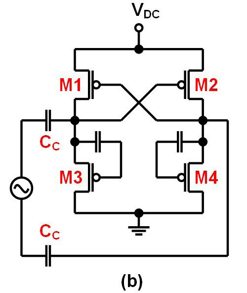
1090                                                                              IEEE TRANSACTIONS ON ELECTRON DEVICES, VOL. 68, NO. 3, MARCH 2021

                                TABLE I
      O RGANIC -TFT PARAMETERS E XTRACTED AND E MPLOYED FOR THE
                         C IRCUIT S IMULATIONS

    contacts of M3 onto the FG, which produces an effect similar
    to a shift of the threshold voltage of M1 toward more positive
    values. To discharge the FG, a negative erase voltage Verase
    is applied, as shown in Fig. 1(f). After disconnecting M3,
    the FG cell can then be operated as a transdiode, with the
    voltage being applied between the source and drain terminals
    of M1, denoted by (Vdiode ), drawing current (Idiode ), as shown
    in Fig. 1(g).
       The measured and simulated current–voltage characteristics
    of the FG cell when operated as a transdiode following erasing
    and programming with different programming voltages are
    shown in Fig. 2(a). Each of the current–voltage curves in
    Fig. 2(a) was recorded in a three-step procedure. First, the FG
    was discharged by applying an erase voltage (Verase) of −3 V
    for a period of 60 s. Second, the FG was charged by applying
    a programming voltage (Vprog ) of 1, 2, 3, or 4 V for a period
    of 60 s (or by not applying a programming voltage at all,
    labeled as “Vprog = 0 V in Fig. 2(a).” Finally, the FG cell was
    operated as a transdiode, as shown in Fig. 1(g), by measuring
    the current (I ) as a function of the applied voltage (V ).
    From Fig. 2(a), the equivalent threshold voltages of −0.5,
    1.0, 1.5, 2.0, and 2.6 V are extracted after programming
    the FG cell with the programming voltages of 0, 1, 2, 3,
    and 4 V, respectively; these values are also summarized in
    the legend in Fig. 2(a). Simulations were performed using a
    compact dc model [13], and the parameters extracted for the
    p-channel DNTT TFTs are summarized in Table I. By per-
    forming the simulations using the threshold voltages extracted
    from Fig. 2(a), good agreement between measurement data
    and simulation results was achieved for each programming                           Fig. 3. Differential rectifiers with dynamic-threshold-voltage compen-
    voltage, indicating successful programming of the FG cell. The                     sation. (a) Circuit diagram when M3 and M4 are implemented as
    discrepancies observed between the measured and simulated                          diode-connected transistors. (b) Circuit diagram when M3 and M4 are
                                                                                       implemented as FG cells. (c) DC output voltage of both circuits measured
    current–voltage curves for the programming voltages of 0                           for a sinusoidal input voltage with an amplitude of 2 V. For the circuit in
    and 4 V are ascribed to photocurrents and onset of dielectric                      which M3 and M4 were implemented as FG cells, the measurements
    breakdown, respectively. Fig. 2(b) shows that the dependence                       were performed after the FG had been charged with programming
                                                                                       voltages (Vprog ) of 0, 1, 2, 3, or 4 V. (d) Output ripple as a function of
    of the threshold voltage on the programming voltage is approx-                     frequency. The four TFTs M1–M4 have the channel length of 10 µm and
    imately linear, with a slope of 0.5.                                               the channel width of 200 µm. FG cells are sized accordingly.
       The charge-retention characteristics of the FG cell are
    shown in Fig. 2(c). For these measurements, the FG was
    discharged with an erase voltage of −3 V and then charged                          (reverse) current, the cause of which will require further
    with a programming voltage of 3 V. The current–voltage                             investigation.
    characteristics were then measured immediately after program-
    ming and again four days later. As can be seen, the dif-                                                     IV. FG R ECTIFIERS
    ference in the forward currents measured immediately after                            The design of efficient rectifiers would benefit from the
    programming and four days later is very small, only about                          availability of high-quality Schottky diodes [14]. Both in
    4%. There is, however, a significant increase in the leakage                       silicon CMOS and in flexible organic electronics, the lack

Authorized licensed use limited to: Max-Planck-Institute Stuttgart Bibliothek Buesnau. Downloaded on February 25,2021 at 10:36:50 UTC from IEEE Xplore. Restrictions apply.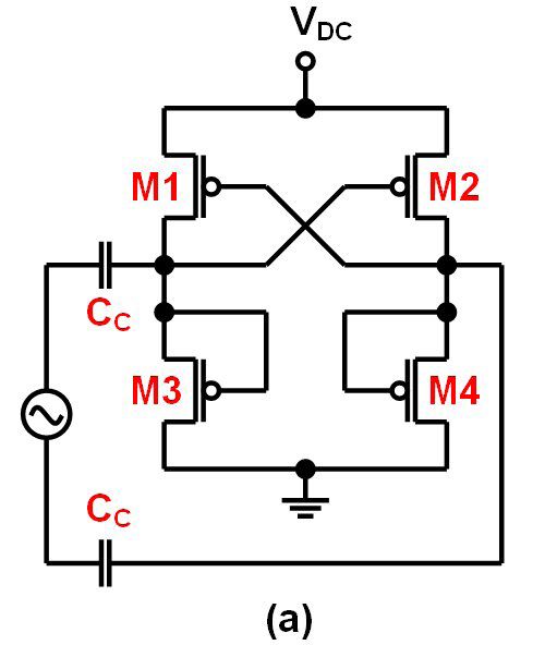
MANSOUR et al.: THREE-TERMINAL FG CELL FOR THRESHOLD-VOLTAGE CONTROL OF ORGANIC TFTs                                                                         1091

    Fig. 4.      Inverters with transdiode load. (a) Circuit diagram of a
    conventional diode-load inverter. (b) Circuit diagram of the proposed FG-
    transdiode-load inverter. (c) Photograph of the proposed FG-transdiode-
    load inverter. (d) Transfer characteristics of both inverters measured for
    a supply voltage of 3 V. In the case of the inverter with the FG-transdiode        Fig. 5. Evaluation of the noise margins of (a) conventional diode-load
    load, the measurement was performed after the FG had been charged                  inverter and (b) proposed FG-transdiode-load inverter.
    with a programming voltage (Vprog ) of 3 V. Mdrive has a channel length
    of 10 µm and a channel width of 600 µm; all other dimensions are                   a flatter frequency response and an improved 3-dB point. The
    identical to those in Fig. 1 (a) (d).
                                                                                       best compromise between dc output voltage and ac ripple is
                                                                                       obtained for a programming voltage (Vprog ) of 1 V. Larger
    of such diodes is compensated for by the use of diode-                             programming voltages cause a shift of the threshold voltage
    connected transistors (transdiodes). This necessitates some                        of M3 and M4 to positive values, resulting in excessive leakage
    form of threshold-voltage compensation to account for the                          and greater ripple.
    higher threshold voltage of rectifiers based on transdiodes,
    compared to rectifiers based on Schottky diodes. An example                                V. P ROGRAMMABLE D IODE -L OAD I NVERTERS
    is dynamic threshold-voltage cancellation, which minimizes                            Unipolar logic gates require load devices, the design of
    the effective threshold voltage in the forward direction while                     which often involves compromises between the various sta-
    maximizing it in the reverse direction for reduced leakage.                        tic and dynamic inverter-performance characteristics. Load
    This concept was initially proposed for silicon CMOS tech-                         designs for unipolar logic include the transdiode load [see
    nology [9], [15] and recently demonstrated with organic TFTs                       Fig. 4(a)], the zero-gate-source voltage (VGS) load, and the
    [16]. The circuit diagram of a single-stage differential-drive                     biased load; examples for more complex designs include the
    dynamic-threshold-voltage-compensated rectifier implemented                        pseudo-CMOS and the bootstrap designs [3], [5], [7], [17]–
    using organic TFTs is shown in Fig. 3(a).                                          [19]. Replacing the conventional transdiode load with an FG
       By replacing the diode-connected M3 and M4 in Fig. 3(a)                         cell makes it possible to control the threshold voltage of the
    with FG cells, as shown in Fig. 3(b), the threshold voltage can                    load and to switch it between enhancement- and depletion-
    be further reduced. Fig. 3(c) shows the dc output voltage of                       mode behavior, with the potential of alleviating some of the
    both circuits measured for a sinusoidal input voltage with an                      compromises between the inverter parameters.
    amplitude (peak-to-peak voltage Vpp ) of 2 V and frequencies                          The circuit diagram of a conventional diode-load inverter is
    ranging from 1 kHz to 30 MHz. For the circuit in which                             shown in Fig. 4(a); the circuit diagram and the layout of the
    M3 and M4 were implemented as FG cells, the measurements                           proposed FG-transdiode-load inverter are shown in Fig. 4(b).
    were performed after the FGs had been charged with pro-                            Transistor M1 in the FG cell that constitutes the load transistor
    gramming voltages (Vprog ) of 0, 1, 2, 3, or 4 V. In Fig. 3(d),                    Mload of the inverter has a channel width of 60 µm, while the
    the ripple is plotted as a function of frequency. The only                         drive transistor Mdrive has a channel width of 600 µm. Both
    smoothing capacitors are the parasitic capacitance inherent to                     have a channel length of 10 µm. Fig. 4(c) shows the measured
    the circuit layout with a value of 100 pF and the capacitance                      transfer characteristics of a conventional diode-load inverter
    of the measurement equipment with a value of 13 pF for                             and the proposed FG-transdiode-load inverter. For the latter,
    both circuits in Fig. 3(a) and (b). Comparing the results                          the measurement was performed after charging the FG with
    obtained for the two circuits, the circuit in Fig. 3(b) provides                   a programming voltage (Vprog ) of 3 V. Comparing the results

Authorized licensed use limited to: Max-Planck-Institute Stuttgart Bibliothek Buesnau. Downloaded on February 25,2021 at 10:36:50 UTC from IEEE Xplore. Restrictions apply.
1092 IEEE TRANSACTIONS ON ELECTRON DEVICES, VOL. 68, NO. 3, MARCH 2021
obtained for the two inverters, the proposed FG-transdiode- [5] S. De Vusser, J. Genoe, and P. Heremans, “Influence of transistor
load inverter provides a larger output–voltage swing (2.8 V parameters on the noise margin of organic digital circuits,” IEEE Trans.
Electron Devices, vol. 53, no. 4, pp. 601–610, Apr. 2006, doi: 10.1109/
versus 2.1 V) and a higher small-signal gain (9 instead TED.2006.870876.
of 3). The evaluation of the noise margins of both inverters [6] P. A. Bobbert, A. Sharma, S. G. J. Mathijssen, M. Kemerink, and
according to the maximum equal criterion [3], [5] is shown D. M. de Leeuw, “Operational stability of organic field-effect transis-
tors,” Adv. Mater., vol. 24, no. 9, pp. 1146–1158, Mar. 2012, doi:
in Fig. 5, yielding the noise margins of 100 and 200 mV for 10.1002/adma.201104580.
the conventional inverter and the proposed FG-transdiode-load [7] K. Myny et al., “Unipolar organic transistor circuits made robust by
inverter, respectively. dual-gate technology,” IEEE J. Solid-State Circuits, vol. 46, no. 5,
pp. 1223–1230, May 2011, doi: 10.1109/JSSC.2011.2116490.
[8] T. Yokota et al., “Control of threshold voltage in low-voltage organic
VI. C ONCLUSION complementary inverter circuits with floating gate structures,” Appl.
Phys. Lett., vol. 98, no. 19, May 2011, Art. no. 193302, doi: 10.1063/
A circuit-level approach for controlling the threshold volt- 1.3589967.
age of organic TFTs operated in the transdiode configuration [9] C. Peters, J. Handwerker, F. Henrici, M. Ortmanns, and Y. Manoli,
“Experimental results on power efficient single-poly floating gate
has been presented. Rather than modifying the transistor rectifiers,” in Proc. IEEE Int. Symp. Circuits Syst., May 2009,
structure, the functionality of an FG is implemented by using pp. 1097–1100, doi: 10.1109/ISCAS.2009.5117951.
two additional TFTs so that the resulting three-terminal FG [10] U. Zschieschang, V. P. Bader, and H. Klauk, “Below-one-volt
organic thin-film transistors with large on/off current ratios,” Organic
cell emulates an organic-TFT-based transdiode with built-in Electron., vol. 49, pp. 179–186, Oct. 2017, doi: 10.1016/j.orgel.
threshold-voltage control. The penalty compared to circuits 2017.06.045.
based on transistors with a built-in additional gate electrode [11] U. Zschieschang and H. Klauk, “Low-voltage organic transistors with
steep subthreshold slope fabricated on commercially available paper,”
is a larger circuit area, which is acceptable for large-area Organic Electron., vol. 25, pp. 340–344, Oct. 2015, doi: 10.1016/
application scenarios. The ability to control the threshold j.orgel.2015.06.038.
voltage of organic TFTs may also be useful to counteract [12] U. Zschieschang, J. W. Borchert, M. Geiger, F. Letzkus, J. N. Burghartz,
and H. Klauk, “Stencil lithography for organic thin-film transistors with
device degradation caused by aging and bias stress. a channel length of 300 nm,” Organic Electron., vol. 61, pp. 65–69,
Oct. 2018, doi: 10.1016/j.orgel.2018.06.053.
ACKNOWLEDGMENT [13] S. Elsaegh, U. Zschieschang, J. W. Borchert, H. Klauk, H. Zappe,
and Y. Manoli, “Compact DC modeling of organic thin-film transistors
The authors would like to thank Prof. Yiannos Manoli including their parasitic non-linear contact effects based on a novel
for his support and the Fritz-Huettinger Foundation for the extraction method,” IEEE Trans. Electron Devices, vol. 66, no. 11,
pp. 4907–4914, Nov. 2019, doi: 10.1109/TED.2019.2941438.
financial contribution. [14] S. Steudel et al., “50 MHz rectifier based on an organic diode,” Nature
Mater., vol. 4, no. 8, pp. 597–600, Jul. 2005, doi: 10.1038/nmat1434.
R EFERENCES [15] K. Kotani, A. Sasaki, and T. Ito, “High-efficiency differential-drive
CMOS rectifier for UHF RFIDs,” IEEE J. Solid-State Circuits, vol. 44,
[1] A. Yamamura et al., “High-speed organic single-crystal transistor no. 11, pp. 3011–3018, Nov. 2009, doi: 10.1109/JSSC.2009.2028955.
responding to very high frequency band,” Adv. Funct. Mater., vol. 30, [16] G. H. Ibrahim, U. Zschieschang, H. Klauk, and L. Reindl, “High-
no. 11, Mar. 2020, Art. no. 1909501, doi: 10.1002/adfm.201909501. frequency rectifiers based on organic thin-film transistors on flexible sub-
[2] J. W. Borchert et al., “Flexible low-voltage high-frequency organic thin- strates,” IEEE Trans. Electron Devices, vol. 67, no. 6, pp. 2365–2371,
film transistors,” Sci. Adv., vol. 6, no. 21, May 2020, Art. no. eaaz5156, Jun. 2020, doi: 10.1109/TED.2020.2989730.
doi: 10.1126/sciadv.aaz5156. [17] M. Elsobky et al., “A digital library for a flexible low-voltage organic
[3] D. Raiteri, P. van Lieshout, A. van Roermund, and E. Cantatore, thin-film transistor technology,” Organic Electron., vol. 50, pp. 491–498,
“Positive-feedback level shifter logic for large-area electronics,” IEEE Nov. 2017, doi: 10.1016/j.orgel.2017.08.028.
J. Solid-State Circuits, vol. 49, no. 2, pp. 524–535, Feb. 2014, doi: 10. [18] T.-C. Huang et al., “Pseudo-CMOS: A design style for low-cost and
1109/JSSC.2013.2295980. robust flexible electronics,” IEEE Trans. Electron Devices, vol. 58, no. 1,
[4] T. Zaki et al., “A 3.3 v 6-bit 100 kS/s current-steering digital-to-analog pp. 141–150, Jan. 2011, doi: 10.1109/TED.2010.2088127.
converter using organic P-type thin-film transistors on glass,” IEEE J. [19] M. Seifaei et al., “Modified bootstrap switching scheme for organic
Solid-State Circuits, vol. 47, no. 1, pp. 292–300, Jan. 2012, doi: 10. digital integrated circuits,” IEEE Solid-State Circuits Lett., vol. 2, no. 10,
1109/JSSC.2011.2170639. pp. 219–222, Oct. 2019, doi: 10.1109/LSSC.2019.2944854.
Authorized licensed use limited to: Max-Planck-Institute Stuttgart Bibliothek Buesnau. Downloaded on February 25,2021 at 10:36:50 UTC from IEEE Xplore. Restrictions apply.You can also read