Tollens Reaction-Based Integration of Thin Film Wall Electrodes into Microfluidic PDMS Devices
←
→
Page content transcription
If your browser does not render page correctly, please read the page content below
Research Article
www.advmattechnol.de
Tollens Reaction-Based Integration of Thin Film Wall
Electrodes into Microfluidic PDMS Devices
Georg Linz, Sebastian Bernhard Rauer, Lucas Stüwe, Daniel Josef Bell, Markus Rausch,
and Matthias Wessling*
metal layer on the bottom of a microflu-
The integration of electrodes into microfluidic devices is a prerequisite for idic channel, which can serve as an elec-
several key technologies such as electrophoresis, dielectrophoresis, elec- trode.[4–6] This well-established method has
the drawback of limiting the visible area for
trowetting, or analysis and manipulation of biological cells in organ-on-a-chip
microscopic analysis while also demanding
applications. However, conventional sputtering or metal deposition methods specific cleanroom facilities for fabrication.
result in electrodes on the top or the bottom of the microfluidic device leading Additionally, the resulting floor-electrodes
to either an inhomogeneous electrical field or considerable restrictions lie in one plane generating an inhomoge-
regarding optical analysis methods. Here, a novel method for integrating elec- neous electric field that exhibits an expo-
trodes into microfluidic devices based on the deposition of silver films on the nential decrease in field strength with
increasing channel height.[4] Floor elec-
sidewalls of microfluidic channels by Tollens reaction is presented. Aldehydes
trodes placed outside of the visual window
diffuse readily through polydimethylsiloxane walls and reduce noble metal may allow optical analysis but lead to sub-
ions such as silver, which in turn precipitate and deposit on the phase border stantial attenuation of the electric field,
as homogeneous thin layers. The process results in sidewall electrodes that whereby separation methods lose efficiency
adopt the channel’s geometry and offer a highly homogeneous electrical field and analysis methods lose precision.[7]
An alternative to the photolithographic
in the case of a rectangular channel. The electrodes were analyzed by dissipa-
fabrication method of planar electrodes is
tive X-ray (EDX) and electrical impedance spectroscopy, while the electrical the integration of wall electrodes. These
field was visualized by particle image velocimetry. The method can fabricate electrodes are positioned perpendicular to
electrodes in different shapes rendering the process highly promising for the visual field and possess superior proper-
a wide range of different electrochemical applications in the field of micro ties concerning the resulting electrical field’s
fluidics, while simultaneously enable optical analysis methods. strength and homogeneity. The voltage
drop is less pronounced, and the dielectro-
phoretic (DEP) force is independent of the
1. Introduction channel height.[7,8] Additionally, the visual window is accessible
for optical analysis, such as microscopic observation. Different
Microfluidic applications that require an electric field such as methods for the introduction of wall electrodes were already pre-
the investigation of electrochemical reactions,[1] electrical detec- sented in the literature. Common techniques include the inser-
tion,[2] or electro-osmosis[3] must consider how electrodes can tion of metal wires into microfluidic devices[9] or the injection of
be integrated into microfluidic devices. The standard method conductive substances into spatially separated channels.[10] While
for electrode integration is a combination of photolithography, wiring requires high precision regarding the correct electrode
sputtering, and lift-off processes. These techniques lead to a thin alignment, spatial separation substantially weakens the electric
field due to voltage loss inside the wall. Even though alternative
processes such as the doping of polydimethylsiloxane (PDMS)
G. Linz, Prof. M. Wessling with conductive particles[11,12] or the penetration-based introduc-
DWI Leibniz-Institute for Interactive Materials tion of liquid bismuth alloys into microfluidic devices demon-
Forckenbeckstrasse 50, 52074 Aachen, Germany
strate feasible alternatives,[5] the development of a simple and
S. B. Rauer, L. Stüwe, D. J. Bell, M. Rausch, Prof. M. Wessling
reproducible manufacturing method for the integration of wall
RWTH Aachen Universtiy, Chemical Process Engineering
Forckenbeckstrasse 51, 52074 Aachen, Germany electrodes still constitutes a major challenge for current research.
E-mail: Manuscripts.cvt@avt.rwth-aachen.de Here, we present a novel and highly reproducible in situ
method for the integration of wall electrodes within microflu-
The ORCID identification number(s) for the author(s) of this article idic PDMS devices, which neither require the doping of PDMS
can be found under https://doi.org/10.1002/admt.202100250.
nor the use of an additional lithographic step. The procedure is
© 2021 The Authors. Advanced Materials Technologies published by Wiley- based on the Tollens reagent, which was introduced by Bern-
VCH GmbH. This is an open access article under the terms of the Creative hard Tollens in 1882 as a method for the detection of alde-
Commons Attribution License, which permits use, distribution and repro-
duction in any medium, provided the original work is properly cited.
hydes in aqueous solutions and was later used to distinguish
between reductive and non-reductive sugars.[13] The Tollens rea-
DOI: 10.1002/admt.202100250 gent applied for the reaction consists of silver nitrate, sodium
Adv. Mater. Technol. 2021, 2100250 2100250 (1 of 7) © 2021 The Authors. Advanced Materials Technologies published by Wiley-VCH GmbH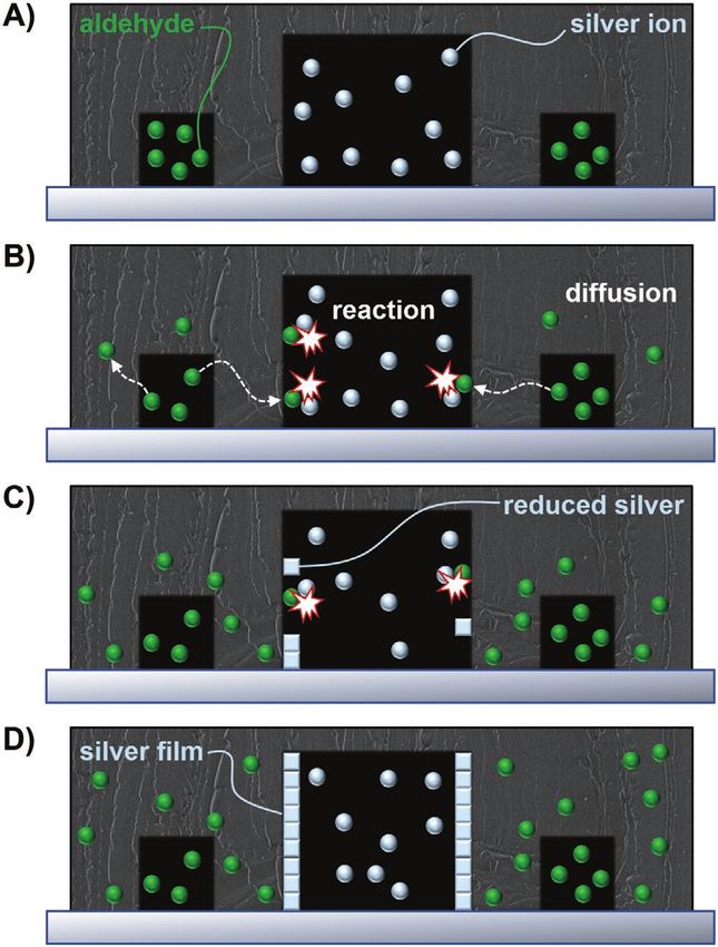
www.advancedsciencenews.com                                                                                                     www.advmattechnol.de

hydroxide, and ammonia, forming diamine silver complexes as
the reactive species. When these complexes are exposed to the
redox reactive aldehyde group (−CHO), the silver ions Ag+ are
reduced to elemental silver, which precipitates on the walls of
the reaction container.[14] The sum of reactions can be written as
RCHO + 2[Ag(NH3)2]+ + 2OH− → 2 Ag↓ + RCOOH + H2O + 4 NH3.
   Contrary to the original reaction, however, the reactants in
our case are spatially separated by a semipermeable PDMS
membrane restricting the reduction reaction to the phase
border. Aldehydes can diffuse readily through PDMS, causing
the deposition of thin film silver electrodes on the channel
walls. The diffusion with a constant concentration source can
be described by

       x2
D=                                                                 (1)
      2× t

where D is the diffusion coefficient in m2 s−1, x the diffusion length
in m and t the time in s.[15] This relationship suggests that the time
required for a species to travel a certain distance x by diffusion is
proportional to the square of the distance itself. As a result, the
initiation time of a diffusion-limited interfacial reaction depends
on the distance of the source to the interface. This principle can be
harnessed to gain control over the site of metal deposition in the
context of electrode integration by an interfacial reduction reac-
tion. By increasing the central channel’s height in relation to the
side channels, the reduction agent requires more time to diffuse
to the channel ceiling than to the wall of the microfluidic channel.
A well-chosen termination time finally results in thin film wall
electrodes directly located within the channel of interest.
                                                                            Figure 1. The concept of reactive integration of silver film electrodes by
                                                                            Tollens reaction in PDMS-based microfluidic chips. A) Cross-section of
                                                                            the microfluidic chip featuring two aldehyde containing side channels and
2. Results and Discussions                                                  a Tollens reagent containing central channel. B) Initiation of the Tollens
                                                                            reaction at the central channel’s wall by diffusion of aldehyde molecules.
The basis for integrating silver film electrodes into microflu-             C) Deposition of reduced silver ions on the channel walls. D) Formation
                                                                            of thin silver films on the channel walls.
idic PDMS chips by Tollens reaction is a specific channel layout
featuring three parallel channels in close proximity (Figure 1).
In this configuration, the Tollens reagent is supplied via the              to the channel ceiling and suppresses premature electrode
central channel, while the side channels are used for aldehyde              fusion.[16] As a result, the silver film electrodes slowly grow
injection (Figure 1A). Considering that PDMS is highly perme-               from the glass bottom upward to the channel ceiling. A well-
able for aldehydes, these molecules will readily sorb into the              chosen termination time for the reaction inhibits the wall elec-
surrounding PDMS matrix and non-directionally diffuse along                 trodes from fusing. In the case of a 4:1 height ratio, time limits
the concentration gradient. Aldehydes that reach the central                between 1 and 10 min were determined to be optimal.
channel and desorb into the Tollens reagent reduce diamine                     Considering the large variety of different aldehydes and
silver complexes to elementary silver, which in turn deposits               their unique interactions with PDMS and the Tollens reagent,
on the microfluidic channel walls (Figure 1B,C). Since aldehyde             the effects of formaldehyde, glutaraldehyde, and benzaldehyde
molecules at the phase border are continuously converted by                 regarding the electrode integration process were investigated.
the Tollens reaction and excess molecules are removed by con-               Figure 2 demonstrates the results of the coating procedure for
tinuous fluid motion, the concentration gradient between the                the corresponding aldehydes as a function of time, where the
channels is maintained. As a result, a thin silver film is depos-           first row of images presents the top view of one half of the
ited onto the central channel’s walls over time (Figure 1D).                microfluidic chip at 1 min, while the second row shows the iden-
Continuous fluid motion and different channel heights are a                 tical section at 3 min. During the experiment, all fluids were in
necessity of the procedure to control the silver deposition along           continuous motion, and parameter variation was restricted to
the z-axis and hence restrict the electrode growth to the chan-             the type of aldehyde. Microscopic analysis revealed that after 1
nel’s wall in an otherwise undirected diffusion process. By                 min, all microfluidic setups show noticeable optical changes. In
increasing the height of the central channel in relation to the             the case of formaldehyde and benzaldehyde, a moderate dark-
side channels, the aldehyde molecules require more time to dif-             ening of the central channels’ wall can be observed, indicating
fuse to the channel ceiling than to the side walls. The laminar             the onset of a successful silver deposition. In contrast, the
flow of Tollens reagent prevents transport of reduced silver                introduction of glutaraldehyde leads to integral changes in the

Adv. Mater. Technol. 2021, 2100250     2100250 (2 of 7)                  © 2021 The Authors. Advanced Materials Technologies published by Wiley-VCH GmbH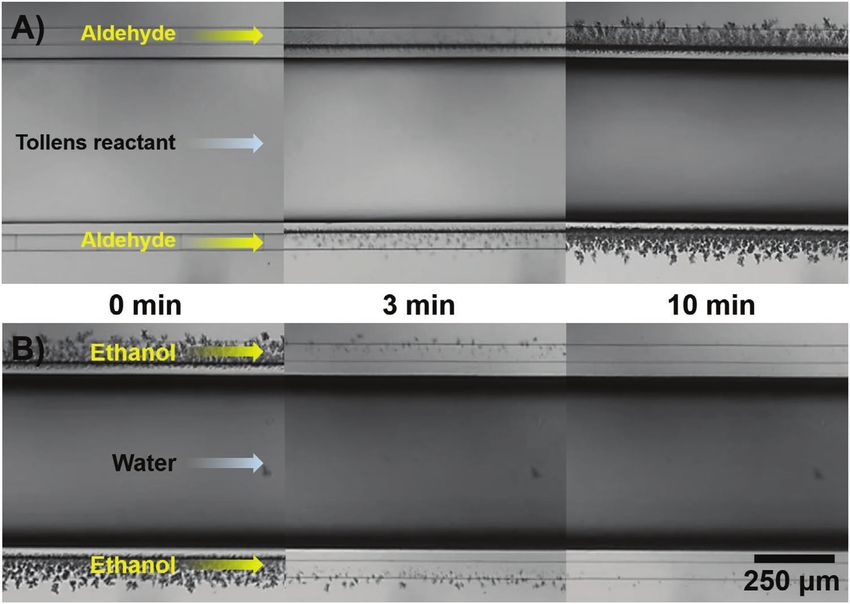
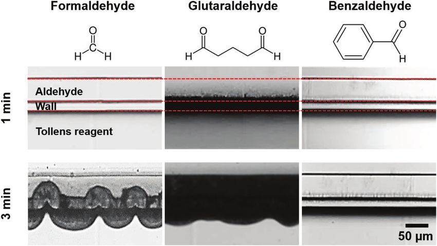
www.advancedsciencenews.com                                                                                                          www.advmattechnol.de

Figure 2. Microscopic analysis of the suitability of different aldehydes with regard to silver deposition by Tollens reaction within a microfluidic PDMS chip.
Formaldehyde concentration: 12.5 wt%, glutaraldehyde concentration: 50 wt%, benzaldehyde concentration: 99.5 wt%. Aldehyde flow rate: 10 cm s−1,
Tollens reagent flow rate: 1.67 cm s−1.

PDMS membrane. The wall swells up to 50% compared to the                         experimental data applying the silver film electrodes, the crystal-
non-wetted state and turns completely opaque, suggesting the                     line by-product has to be removed from the microfluidic setup.
accumulation of by-products within the membrane. For glutar-                     For this purpose, ethanol has proven to be a suitable solvent to
aldehyde, this swelling increases steadily up to the 3 min mark,                 dissolve the precipitated crystals, as showcased in Figure 3B.
at which point the swelling reaches factors of 2 to 2.5 and by-                     Moreover, it should be mentioned that continuous fluid
product precipitations expands into the side channels. Similar to                motion above a certain velocity threshold constitutes a major
glutaraldehyde, the membrane also swells significantly after pro-                necessity of the electrode coating process. In this context,
longed contact with formaldehyde. The swelling causes increases                  experiments could demonstrate that a dormant or low-velocity
in wall diameter of up to 200% (factor of 3) and results in major                Tollens reagent leads to the precipitation of a crystalline sub-
membrane corrugations. In the case of benzaldehyde, even after                   stance within the central channel (Figure S2, Supporting
3 min of reaction, no substantial membrane alterations can be                    Information). This effect seems to be related to the removal of
detected. Substance deposition in the vicinity of the central chan-              ammonia from the Tollens reagent by diffusion into the sur-
nels’ walls intensifies, while minor precipitation of transparent                rounding PMDS matrix and occurs at Tollens reagent velocity
crystals can be observed in the aldehyde channels. This result                   below 0.5 cm s−1. The decrease of ammonia can lead to the
agrees well with the fact that aromatic aldehydes are less reac-                 destabilization of silver diamine complexes, resulting in the
tive partners for the Tollens reagent,[14] which in turn improves                precipitation of crystalline silver oxide. The possibility of redis-
process control. Therefore, subsequent investigations on the                     solution by an increase in reactant flow rate or exposure to
integration of wall electrodes were limited to benzaldehyde as a                 ammonia supports this hypothesis.
reducing agent as it demonstrates the best performance in terms                     Considering that even the best electrode cannot be oper-
of unwanted swelling, permeability, and silver reduction.                        ated without an appropriate electrical connection, the basic
   The complete coating procedure using benzaldehyde is                          three-channel layout of the microfluidic chip had to be
depicted in Figure 3 as a time series of microscopy pictures,                    extended by two contacting chambers (Figure 4A). These two
where Figure 3A) shows the chronological sequence of the Tol-                    914 (W) × 200 (H) μm geometries enable the introduction
lens reaction, while Figure 3B) demonstrates the cleaning pro-                   liquid contacting substances such as silver conductive lacquer
tocol for the removal of the crystalline by-products from the                    by capillary force. The contacting chambers are attached to the
PDMS walls and side channels. At the time t = 0 min, the two                     500 (W)×200 (H) μm central channel by two 57 (W) × 200 (H)
reagents are fed into the corresponding channels to initiate the                 μm junctions. These channel constrictions were implemented
reaction. At this stage, the microfluidic channels are entirely                  to substantially increase the flow resistance and allow for
transparent, and no visual changes can be detected. After 3 min,                 more precise control over the contacting substance’s penetra-
the previously described phenomena occur. Silver is depos-                       tion depth. To establish a reliable electrical contact to the silver
ited in close proximity to the wall along the central channel,                   film electrodes, the 50 (W) × 50 (H) μm aldehyde side channels
and transparent crystals form within the side channels. Both                     were not only guided in parallel to the desired electrode posi-
effects steadily intensify over time until the aldehyde channels                 tion but also to the junction channels as well as the inner sec-
are finally severely obstructed by side-product, and the onset                   tion of the contacting chambers at a distance of 40 μm. Silver
of silver deposition can be detected as a minor discoloration                    deposition within the respective parts provided an extensive
at the ceiling of the central channel. To prevent falsification of               contacting area for the silver conductive lacquer outside the

Adv. Mater. Technol. 2021, 2100250         2100250 (3 of 7)                  © 2021 The Authors. Advanced Materials Technologies published by Wiley-VCH GmbH
www.advancedsciencenews.com                                                                                                       www.advmattechnol.de

Figure 3. Overview of the coating procedure using benzaldehyde. A) Time sequence of microscopy images presenting the progression of silver deposi-
tion in the central channel and the formation of a crystalline side product in the side channels. B) Removal of the reactants and crystalline side product
by water and ethanol flush.

central channel (Figure S3, Supporting Information). This intri-               featuring coated silver film electrodes and fully functional elec-
cate layout design enabled the integration of electrical connec-               trical connections integrated into the contacting chambers via
tions to the silver film electrodes by means of Tollens reaction               silver conductive lacquer is presented in Figure 4B.
already during the coating process. To minimize the number of                     The connection to the electrode assembly was probed with
syringe pumps necessary for the setup operation, the side chan-                electrical impedance spectroscopy (EIS). The Bode plot of the
nels were interconnected by tubing according to the numerical                  EIS spectra in Figure 5 shows the modulus and phase shift
sequence indicated in Figure 4A). The aldehyde was initially                   of the impedance above the frequency. In the high-frequency
injected into position 0 from where it flowed along the respec-                range (above 104 Hz), no significant phase-shift between voltage
tive channel toward position 1. Position 1 was subsequently                    and current can be observed, representing the electrode and
connected to position 2 via a Smith Medical Portex Fine Bore                   electrolyte’s resistance. Below 104 Hz the forming ionic double-
LDPE Tubing (0.38 mm ID, 1.09 mm OD) and finally excited                       layer on the electrode–electrolyte interfaces increase the imped-
at position 3, where it was collected in a waste container. This               ance with decreasing frequency. The electrical double-layer
interconnection of the aldehyde channels was repeated on the                   can be modeled with a constant phase element (CPE).[17] Since
opposite side of the chip. The general flow direction of all reac-             both electrodes are from the same material, both electrode–
tants is indicated in Figure 4A. An overview of the final product              electrolyte interfaces can be modeled with one CPE.

Figure 4. The layout of the microfluidic chip. A) Scheme of the general chip structure as CAD top-view; green: Tollens reagent channel and contacting
chambers; yellow: aldehyde channels; circles: Tubing insertion points. B) Microscopy image of a complete chip coated with silver film electrodes.

Adv. Mater. Technol. 2021, 2100250        2100250 (4 of 7)                 © 2021 The Authors. Advanced Materials Technologies published by Wiley-VCH GmbH
www.advancedsciencenews.com www.advmattechnol.de
microscope features a hybrid detector allowing for both the
detection of secondary and backscattered electrons, brightness
differences can be directly correlated to detecting different ele-
ments.[18] Heavy elements of high atomic number backscatter
more intensively than light elements of low atomic number
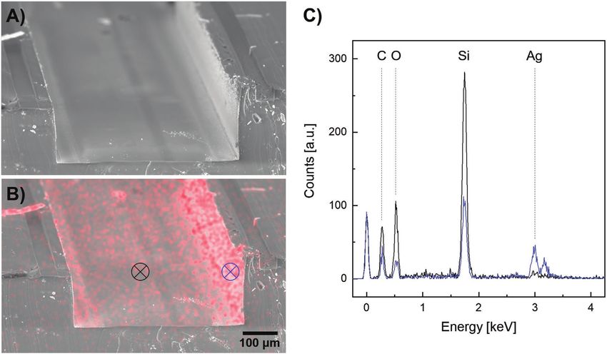
and appear brighter in the resulting image. In Figure 6 A the
channel wall appears considerably brighter than the channel
ceiling, providing the first indication of a successful spatially
selective coating. Moreover, this result is supported by the EDX
analysis in Figure 6B, which presents the distribution of silver
across the microfluidic channel in red. Figure 6C depicts site-
specific EDX data of the channel ceiling (black) and the channel
wall (blue) for carbon, oxygen, silicon, and silver. Analysis of
the data reveals that the channel ceiling merely presents a silver
content of 3.0 wt%, while the side wall exhibits 39.5 wt% silver.
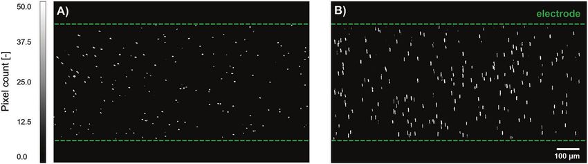
Particle image velocimetry (PIV) enables the in-depth optical
analysis of particle movement within optically transparent
fluids. Figure 7 presents fluorescently labeled polystyrene beads
Figure 5. Bode plot presentation of the EIS measurement of the wall located within the central channel of the microfluidic device in
electrodes in 50 mmol L-1 NaCl solution. The ionic double-layer on the absence (Figure 7A) and presence (Figure 7B) of an applied elec-
electrode–electrolyte interface is fitted with a constant phase element, trical field, where each image constitutes the sum of 20 consecu-
while the electrolyte as well as connectors with a resistor in series. The tive video frames. Considering the usage of spherical beads and
fitting results in R = 1750 Ω ; CPE-Q = 1.42 × 10⁻⁶ sΩ−1; CPE-n = 0.7693. the fact that the particle position is traced over the duration of
20 frames, particle motion become visible as continuous white
To determine whether the deposit within the central channel lines, while dormant beads are observable as white circular
is silver, Tollens-reaction based coating was conducted for 1 min, dots. The alternating electrical field evokes a migration of the
and the resulting microfluidic chip was examined by SEM negatively charged tracer particles toward the counter-charged
and EDX. Figure 6A,B demonstrates the PDMS part of the electrode until the electric double-layer is formed, which leads
micro fluidic device rotated 180°. Since the applied electron to a strong potential drop in the boundary layer. The fact that
Figure 6. Verification and quantification of in-chip silver deposition. A) SEM cross-section image of the microfluidic chip after the coating process.
B) Visual representation of the silver distribution within the microfluidic channel, where silver is depicted in red. C) EDX analysis of channel ceiling
(black) and channel wall (blue).
Adv. Mater. Technol. 2021, 2100250 2100250 (5 of 7) © 2021 The Authors. Advanced Materials Technologies published by Wiley-VCH GmbH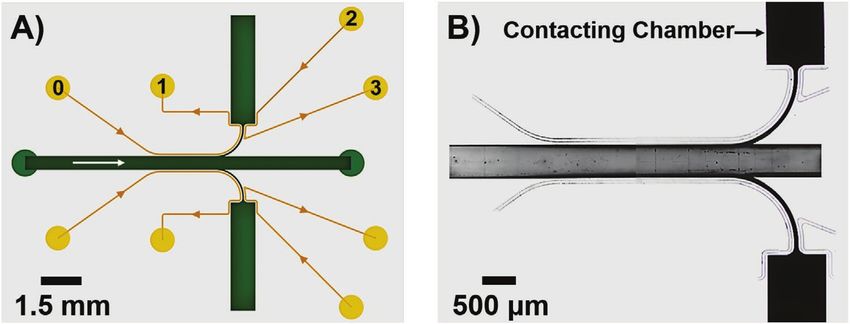
www.advancedsciencenews.com                                                                                                      www.advmattechnol.de

Figure 7. Visualization of the electrical field orientation between thin film silver electrodes inside a microfluidic channel. Each image constitutes the
sum of 20 consecutive video frames. A) Fluorescent tracer particles (white) between thin film silver electrodes in the absence of an electrical field.
B) Fluorescent tracer particles (white) between thin film silver electrodes in the presence of an electrical field.

particle movement occurs exclusively upon the application of                  necessary for the replica was 3D-printed using a multiphoton
voltage proves the presence of fully functional electrodes, while             3D printer (Nanoscribe, Photonic Professional GT). A detailed
the highly specific direction of motion perpendicular to the                  description of the master and chip fabrication procedure can be
                                                                              found in the following publication, ref. [19]. In short, the master used
electrodes emphasizes the homogeneity of the electric field in                for the replica production was designed using the computer-aided
the case of rectangular channel geometries. The particle oscilla-             design (CAD) software Autodesk Inventor 2019 and was 3D-printed
tion can be seen in Video S4, Supporting Information.                         via dip-in laser lithography on microscopy glass substrates (Sigma-
                                                                              Aldrich, 25 × 75 × 1 mm). Before printing, the glass substrates
                                                                              were cleaned in isopropanol (Sigma-Aldrich, ≥99.8 and acetone
                                                                              (Honeywell, ≥99), followed by a silanization in a 3(trimethoxysilyl)
3. Conclusions                                                                propyl acrylate (Sigma-Aldrich, 92 with 100 ppm BHT) solution. The
                                                                              silanized substrates were covered with several photoresist droplets
In this work, we present a facile and highly-reproducible method              (Nanoscribe, IP-S), and the microfluidic master mold was printed
for the integration of versatile wall electrodes into microfluidic            section-wise with rectangular splitting two-photon polymerization.
PDMS devices based on the site-specific reduction of metal                    Subsequently, the master mold was developed in propylene glycol
ions by Tollens reaction. The linchpin of this procedure is the               methyl ether acetate (Sigma-Aldrich, ≥99.5), cleaned in isopropanol,
spatial separation of the reactants by a semipermeable PDMS                   and post-cured by exposure to an ultraviolet light source (302 nm,
                                                                              8 W) for 12 h. For microfluidic chip fabrication, the resulting master
membrane, which exclusively allows for diffusive exchange of
                                                                              mold was covered by PDMS (DowCorning, SylgardŴ184 plus curing
species and hence delays the interaction between reducing alde-               agent 10:1 (w/w)) and cured in an oven overnight at 60 °C. Afterward,
hydes and metal ions. Considering that the length of the diffu-               the solidified PDMS was separated from the master mold, and holes
sion path dictates the arrival time of the reducing agent, the site           for the connecting tubings were punched using biopsy punchers
of metal deposition can be controlled by a difference in channel              (EMS, Rapid-Core 0.75 mm). Finally, the PDMS slab was cleaned by
heights. In this context we demonstrate that aromatic aldhydes                sonication in isopropanol, dried in a desiccator at room temperature
such as benzaldehyde constitute the reducing agent of choice                  and plasma bonded to a microscope glass substrate (Sigma Aldrich,
                                                                              25 × 75 × 1 mm) applying an absolute oxygen pressure of 0.3 mbar
enabling the integration of functional film electrodes in less                (40 mL min-1) at 60 W for 30 s (TePla 100 Plasma System, PVA).
than 10 min. Furthermore, by applying our unique chip design,                     Tollens Reagent: The alkaline silver nitrate solution stabilized by an
it is possible to integrate not only the electrodes, but also the             ammonia complex is also named Tollens reagent. In the first step, the
corresponding electrical leads in just a single step. The success             silver ions were precipitated by mixing a 10 wt% silver nitrate (Sigma
of our method was verified by EIS, EDX, and μPIV measure-                     Aldrich) solution and 1.0 mol L-1 sodium hydroxide solution (Sigma
ments. Since the electrodes adopt the channel wall geometry,                  Aldrich) in a molar ratio of 1. Subsequently, an ammonia solution
                                                                              (5 wt% in DI water) (Sigma Aldrich) was added dropwise until the
the presented electrode integration method can also be used to
                                                                              brown sediment was completely dissolved. Considering that ammonia
generate inhomogeneous electric fields. For example, a mean-                  readily diffuses into PDMS 4 vol% of excess ammonia solution was
dered channel wall geometry would lead to a meandered elec-                   finally added to prevent the precipitation of silver hydroxide or silver
trode, which could be applied for dielectrophoresis. To our                   oxide within the microfluidic chip.
knowledge, this is the first approach using the permeability of                   Silver Film Electrodes by Tollens Reaction: For the deposition of
PDMS toward hydrophilic substances as a possibility to bring a                thin film silver electrodes on the walls of the microfluidic channels,
                                                                              benzaldehyde (99.5%, Sigma-Aldrich) and the Tollens reagent were
reducing agent to metal ions and using this metal as electrodes.
                                                                              introduced into the corresponding channels via a syringe pump
We hope this will help researchers working in microfluidics to                (Chemyx, Fusion 4000) at flow rates of 0.02 and 0.1 mL min-1,
integrate electrodes serving different requirements.                          respectively. To limit the reaction to the channel walls, the initiation of
                                                                              the reactant flows was sequenced. The aldehyde flow was only initiated
                                                                              when the central channel was completely filled with Tollens reagent.
4. Experimental Section                                                       The progression of the Tollens reaction was monitored via a bright
                                                                              field microscope (Leica Microsystems, DMIL LED Fluo). Based on
   Microfluidic Chips by Soft-Lithography: Microfluidic chips were            the extent of silver deposition, the reaction was terminated after 1 to
prepared via PDMS replica molding. The positive master mold                   10 min by replacing the aldehyde with an ethanol flow. Subsequently,

Adv. Mater. Technol. 2021, 2100250        2100250 (6 of 7)                © 2021 The Authors. Advanced Materials Technologies published by Wiley-VCH GmbH
www.advancedsciencenews.com www.advmattechnol.de
the Tollens reagent was removed by flushing the central channel European Research Council (ERC) under the grant agreement no.
with DI water preventing post-reactions at the channel walls due to 694946. Part of the work was performed at the Center for Chemical
residual aldehyde stored within the PDMS. The ethanol and DI-water Polymer Technology CPT, which is supported by the EU and the federal
flush was conducted for at least 60 min at flow rates of 0.02 and state of North Rhine-Westphalia (grant no. EFRE 30 00 883 02).
0.1 mL min-1, respectively. Finally, the microfluidic channels were dried Open access funding enabled and organized by Projekt DEAL.
by applying a constant airflow, and the chip was stored in a fume hood
for 24 h to remove the remaining solvent residues by evaporation.
Electrode Contacting: To contact the silver film electrodes, the
corresponding contacting chambers were opened by a perpendicular Conflict of Interest
cut using a razor blade. Subsequently, silver conductive lacquer (Ferro)
was applied to the openings with a brush, entering the chambers by The authors declare no conflict of interest.
capillary force (Figure S1, Supporting Information). To guarantee
an appropriate contacting area, additional silver conductive lacquer
was spread uniformly between the chamber openings and the edge
of the microscopy slide. The chips were finally dried in atmospheric Data Availability Statement
conditions for at least 1 week to ensure the silver conductive lacquer’s The data that support the findings of this study are available from the
gentle curing. corresponding author upon reasonable request.
Electrical Impedance Spectroscopy: To verify proper electrode
contacting, electrical impedance spectroscopy (EIS) and subsequent
equivalent electric circuit fitting were used. The EIS measurements
were performed in potentiostatic mode with an amplitude of 10 mV and Keywords
at a frequency range of 10 Hz to 100 kHz with ten probes per decade.
A Reference 3000 potentiostat (Gamry Instruments) was used for the 3D electrodes, electrochemical, microfluidic, silver electrodes
electrochemical characterization. The potentiostat’s inputs and outputs
were connected to the silver conductive lacquer by a combination Received: March 1, 2021
of silver plates and crocodile clips to ensure proper contact. The Revised: April 29, 2021
microfluidic channel was filled with 50 mmol L-1 aqueous sodium Published online:
chloride solution as an electrolyte. A CPE in series with a resistor
was chosen as an equivalent electric circuit. The CPE represents the
electrode/electrolyte interface, and the resistor represents the ohmic
resistances of the electrode and electrolyte bulk resistance.
[1] W. B. Zimmerman, Chem. Eng. Sci. 2011, 66, 1412.
SEM and EDX: Morphology, position, and coverage of the deposited
[2] B. S. Ferguson, S. F. Buchsbaum, J. S. Swensen, K. Hsieh, X. Lou,
silver film electrodes were analyzed using scanning electron microscopy
H. T. Soh, Anal. Chem. 2009, 81, 6503.
(SEM) in combination with energy dispersive X-ray (EDX) (Hitachi
High Tech TM 3030Plus). To investigate the chips with SEM and EDX, [3] X. Wang, C. Cheng, S. Wang, S. Liu, Microfluid. Nanofluid. 2009, 6,
the plasma bonded PDMS part of the microfluidic chips was gently 145.
separated from the microscopy slide with a razor blade. [4] L. Rao, B. Cai, X. L. Yu, S. S. Guo, W. Liu, X. Z. Zhao, AIP Adv. 2015,
Particle Image Velocimetry (PIV): A μPIV system (LaVision GmbH) 5, 5.
was applied to demonstrate the electrical field’s homogeneity between [5] S. Li, M. Li, Y. S. Hui, W. Cao, W. Li, W. Wen, Microfluid. Nanofluid.
thin film silver electrodes. Rhodamine B labeled polystyrene tracer 2013, 14, 499.
particles (ThermoFisher Scientific, 0.86 μm) were diluted 1:5000 in [6] M. Li, W. H. Li, J. Zhang, G. Alici, W. Wen, J. Phys. D: Appl. Phys.
1 mmol L-1 KCl solution and were flushed into the channel. To exclude 2014, 47, 6.
the influence of fluid movement on the particles during observation, [7] B. ÇETİN, S. Zeinali, presented at 4th Micro and Nano Flows Conf.,
the in- and outlet of the microfluidic device were sealed after filling. London, UK, September 2014.
The negatively charged tracer particles were subsequently excited [8] K. Y. Lu, A. M. Wo, Y. J. Lo, K. C. Chen, C. M. Lin, C. R. Yang, Bio-
by a potential of 0.4 V with 5 polarity changes per second. Images sens. Bioelectron. 2006, 22, 568.
were taken with a microscope (SteREO Discovery V20 Carl Zeiss [9] L. M. Griep, F. Wolbers, B. De Wagenaar, P. M. Ter Braak,
Microscopy GmbH) using a 24× magnification resulting in a depth B. B. Weksler, I. A. Romero, P. O. Couraud, I. Vermes, A. D. Van Der
of field of 27 μm. Pulsing frequency of the Nd:YAG laser (Photonics Meer, A. Van Den Berg, Biomed. Microdevices 2013, 15, 145.
Industries Inc. DM150-532) was set to 100 Hz. Laser current was [10] T. W. Herling, T. Müller, L. Rajah, J. N. Skepper, M. Vendruscolo,
adjusted at 16 A. The high speed cameras (Phantom VEO710L Vision
T. P. Knowles, Appl. Phys. Lett. 2013, 102, 18.
Research) recorded with 200 fps and an exposure time of 100 μs.
[11] C. Iliescu, G. L. Xu, V. Samper, F. E. Tay, J. Micromech. Microeng.
Image processing was performed via DaVis 10.0.5 (LaVision GmbH)
2005, 15, 494.
Software. For visualization of the particle movement, 20 consecutive
frames were accumulated. [12] X. Niu, S. Peng, L. Liu, W. Wen, P. Sheng, Adv. Mater. 2007, 19, 2682.
[13] B. Tollens, Ber. Dtsch. Chem. Ges. 1882, 15, 1635.
[14] R. Parry-Jones, J. Kumar, Educ. Chem. (London, U. K.) 1985, 22, 114.
Supporting Information [15] R. Bird, W. Stewart, E. Lightfoot, Transport Phenomena, Wiley,
Weinheim, Germany 2001.
Supporting Information is available from the Wiley Online Library or [16] Z. Ge, H. Yan, W. Liu, C. Song, R. Xue, Y. Ren, Micromachines 2020,
from the author. 11, 8.
[17] Y. Feldman, R. Nigmatullin, E. Polygalov, J. Texter, Phys. Rev. E: Stat.
Phys., Plasmas, Fluids, Relat. Interdiscip. Top. 1998, 58, 7561.
Acknowledgements [18] J. I. Goldstein, D. E. Newbury, P. Echlin, D. C. Joy, C. Fiori, E. Lifshin,
G.L. and S.R. contributed equally to this work and share the Scanning Electron Microscopy and X-Ray Microanalysis 1981.
first authorship. M.W. acknowledges the support through the Gottfried [19] J. Lölsberg, J. Linkhorst, A. Cinar, A. Jans, A. J. Kuehne, M. Wessling,
Wilhelm Leibniz award. This project has received funding from the Lab Chip 2018, 18, 1341.
Adv. Mater. Technol. 2021, 2100250 2100250 (7 of 7) © 2021 The Authors. Advanced Materials Technologies published by Wiley-VCH GmbHYou can also read