ULTRA-WIDEBAND MILLIMETER-WAVE ANTENNA ARRAYS AND FRONT-END SYSTEMS - DIVA PORTAL
←
→
Page content transcription
If your browser does not render page correctly, please read the page content below
Digital Comprehensive Summaries of Uppsala Dissertations
                from the Faculty of Science and Technology 2005

                Ultra-wideband Millimeter-wave
                Antenna Arrays and Front-end
                Systems
                For high data rate 5G and high energy physics
                applications

                IMRAN AZIZ

    ACTA
UNIVERSITATIS
 UPSALIENSIS    ISSN 1651-6214
                ISBN 978-91-513-1122-7
  UPPSALA       urn:nbn:se:uu:diva-433095
    2021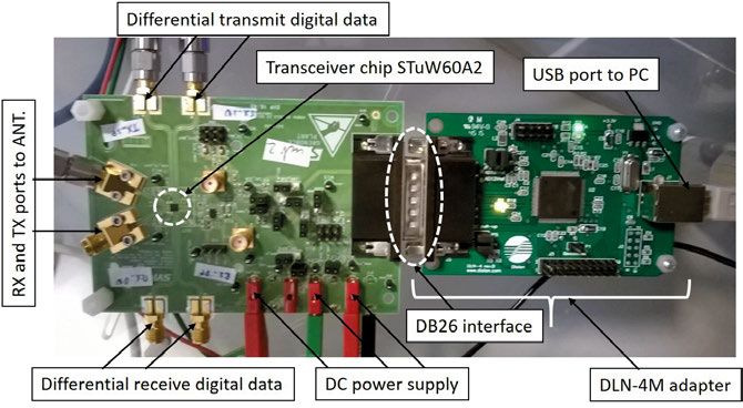
Dissertation presented at Uppsala University to be publicly examined in Polhemsalen,
Ångströmlaboratoriet, Lägerhyddsvägen 1, Uppsala, Monday, 15 March 2021 at 09:15 for
the degree of Doctor of Philosophy. The examination will be conducted in English. Faculty
examiner: Associate Professor Ville Viikari (Aalto University, Finland).

Abstract
Aziz, I. 2021. Ultra-wideband Millimeter-wave Antenna Arrays and Front-end Systems. For
high data rate 5G and high energy physics applications. Digital Comprehensive Summaries
of Uppsala Dissertations from the Faculty of Science and Technology 2005. 68 pp. Uppsala:
Acta Universitatis Upsaliensis. ISBN 978-91-513-1122-7.

The demand for wireless data communications is rapidly increasing due to several factors
including increased internet access, increasingly growing number of mobile users and services,
implementation of the Internet of Things (IoT), high-definition (HD) video streaming and video
calling. To meet the bandwidth requirement of new and emerging applications, it is necessary
to move from the existing microwave bands towards millimeter-wave bands.
   This thesis presents different antenna arrays at 60 GHz and 28 GHz that are integrated with
the front-end RFIC to steer the beam in ≈ ±50° in the azimuth plane. The 5G antenna arrays
at 28 GHz are designed to provide broadband high data rate services to the end users. In order
to transport this high-volume data to the core network, a fixed wireless access (FWA) link
demands the implementation of a broadband, high gain and steerable narrow-beam array. The
60 GHz antenna arrays, presented in this thesis, are good candidates for both FWA as well as
backhaul communications. The two proposed arrays at 60 GHz (57-66 GHz) are i) a stacked
patches array and ii) a connected slots array feeding a high gain lens antenna. The 2×16 stacked
patches antenna array shows more than 20 dBi realized gain. The array is integrated with the
front-end RFIC and the resulting module shows > 40 dBm measured effective isotropic radiated
power (EIRP). The other 60 GHz antenna array is designed as linear connected slots with sixteen
equidistant feeding points. The latest is then used as a feeder of a high gain dielectric lens. Peak
measured gain of 25.4 dBi is achieved with this antenna. Moreover, instead of experiencing scan
loss, the lens is designed to get higher gain when the beam is steered away from the broadside
direction.
   Furthermore, two compact antenna arrays are designed at 28 GHz (24.25 - 29.50 GHz). A
linear polarized (LP) and a circular polarized (CP) array are realized in the fan-out embedded
wafer level ball-grid-array (eWLB) package. In comparison with the PCB arrays, this antenna
in package (AiP) solution is not only cost-effective but it also reduces the integration losses
because of shorter feed lines and no geometrical discontinuity. The LP array is realized as a
dipole antenna array feeding a novel horn-shaped heatsink. The RF module gives 34 dBm peak
EIRP with beam-steering in ±35°. Besides, the CP antenna array is realized with the help of
crossed dipoles and the RF module provides 31 dBm peak EIRP with beam-steering in ±50°.
   The data demands are not limited to the telecom industry as the upgradation of accelerators
and experiments at the large hadron collider (LHC) at CERN will result in increased event
rate thus demanding higher data rate front-end readout systems. This work thus investigates
the feasibility of 60 GHz wireless links for the data readout at CERN. For this purpose, the 60
GHz wireless chips are irradiated with 17 MeV protons [dose 7.4 Mrad (RX) & 4.2 Mrad (TX)]
and 200 MeV electrons [dose 270 Mrad (RX) & 314 Mrad (TX)] in different episodes. The
chips have been found operational in the post-irradiation investigations with some performance
degradation. The encouraging results motivate to move forward and investigate the realization
of wireless links in such a complex environment.

Imran Aziz, Department of Electrical Engineering, Solid-State Electronics, Box 534, Uppsala
University, SE-751 21 Uppsala, Sweden.

© Imran Aziz 2021

ISSN 1651-6214
ISBN 978-91-513-1122-7
urn:nbn:se:uu:diva-433095 (http://urn.kb.se/resolve?urn=urn:nbn:se:uu:diva-433095)
Dedicated to the peace of my heart, my daughter, Amna Aziz,
                           with her birth this journey started
                          And to my sweet son, Hamza Aziz,
                  with whose birth this journey is gonna end.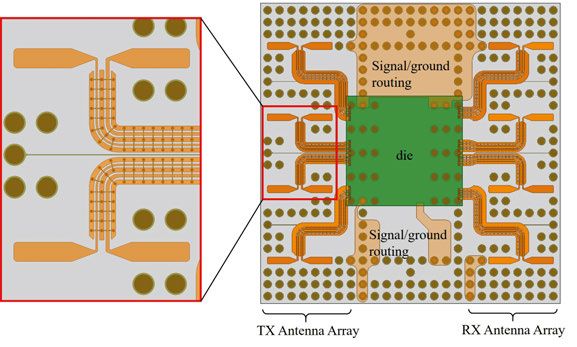
List of papers

This thesis is based on the following papers, which are referred to in the text
by their Roman numerals.

   I   I. Aziz, R. Dahlbäck, E. Öjefors, K. Sjögren, A. Rydberg and D. Dancila,
       60 GHz compact broadband antenna arrays with wide-angle beam
       steering, in The Journal of Engineering, vol. 2019, no. 8, pp. 5407–
       5414, 8 2019, doi: 10.1049/joe.2018.5343.

  II   I. Aziz, D. Dancila, S. Dittmeier, A. Siligaris, C. Dehos, P. Lurgio, Z.
       Djurcic, G. Drake, J. Jimenez, L. Gustaffson, D. Kim, E. Locci, U.
       Pfeiffer, P. Vazquez, D. Röhrich, A. Schöning, H. Soltveit, K. Ullaland,
       P. Vincent, S. Yang and R. Brenner, Effects of proton irradiation on
       60 GHz CMOS transceiver chip for multi-Gbps communication in
       high-energy physics experiments, in The Journal of Engineering, vol.
       2019, no. 8, pp. 5391–5396, 8 2019, doi: 10.1049/joe.2018.5402.

 III   I. Aziz, E. Öjefors and D. Dancila, Connected Slots Antenna Array
       Feeding the High Gain Lens for Wide-angle Beam-steering Applica-
       tions, Accepted for publication in International Journal of Microwave
       and Wireless Technologies (IJMWT).

 IV    I. Aziz, B. Franzen, E. Öjefors and D. Dancila, Broadband beam-
       steerable WiGig module for high data rate access and backhaul
       communications, Manuscript submitted for publication.

 V     I. Aziz, D. Wu, E. Öjefors, J. Hannings, E. Wiklund and D. Dancila, 28
       GHz Compact Dipole Antenna Array Integrated in Fan-out eWLB
       Package, Manuscript submitted for publication.

 VI    I. Aziz, J. Hannings, E. Öjefors, D. Wu, E. Wiklund and D. Dancila, 28
       GHz Circular Polarized Fan-out Antenna Array with Wide-angle
       Beam-steering, Manuscript.

Reprints were made with permission from the publishers.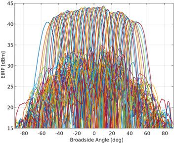
Other publications

Following papers are not included in this thesis because of either overlap or
the contents are outside the scope of this thesis.

   I   I. Aziz, R. Dahlbäck, E. Öjefors, A. Rydberg and D. Dancila, High
       gain compact 57 – 66 GHz antenna array for backhaul & access
       communications, 12th European Conference on Antennas and Propaga-
       tion (EuCAP 2018), London, 2018, pp. 1–4, doi: 10.1049/cp.2018.0362.

  II   I. Aziz, A Rydberg and D Dancila, Electromagnetically Coupled Multi-
       layer Patch Antenna for 60 GHz Communications, GigaHertz Sympos-
       ium, Lund, May 24–25, 2018.

 III   I. Aziz, E. Öjefors, R. Dahlbäck, A. Rydberg, G. Engblom and D.
       Dancila, Broadband Connected Slots Phased Array Feeding a High
       Gain Lens Antenna at 60 GHz, 2019 49th European Microwave Confe-
       rence (EuMC), Paris, France, 2019, pp. 718–721,
       doi: 10.23919/EuMC.2019.8910856.

 IV    I. Aziz on behalf of WADAPT collaboration, Proton Irradiation Hard-
       ness Investigations of 60 GHz Transceiver Chips for High Energy
       Physics Experimentations, poster presented at VCI2019 - The 15th
       Vienna conference on instrumentation, 18–22 Feb, 2019.
       URL: https://indico.cern.ch/event/716539/contributions/3256662/

 V     I. Aziz, W. Liao, H. Aliakbari and W. Simon, Compact and Low Cost
       Linear Antenna Array for Millimeter Wave Automotive Radar App-
       lications, 2020 14th European Conference on Antennas and Propagation
       (EuCAP 2020), Copenhagen, Denmark, 2020, pp. 1–4,
       doi: 10.23919/EuCAP48036.2020.9135772.

 VI    I. Aziz, D. Wu, E. Öjefors, J. Hanning, E. Wiklund and D. Dancila,
       Broadband fan-out phased antenna array at 28 GHz for 5G applica-
       tions, Accepted for EuMW2020.

VII    E. Öjefors, D. Dancila, I. Aziz, J. Hanning, Arrangement comprising
       an integrated circuit package and a heatsink element, Patent applica-
       tion filed, application number EP21150555.7, Jan 2021.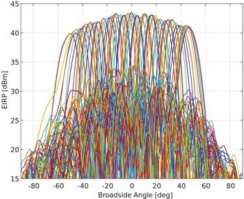
VIII   E. Öjefors, D. Dancila, I. Aziz, J. Hanning, Arrangement comprising
       crossed dipole array integrated in the package, Patent application in
       process.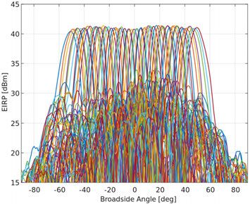
Contents

1   Introduction . . . . . . . . . . . . . . . . . . . . . . . . . . . . . . . . . . . . . . . . . . . . . . . . . . . . . . . . . . . . . . . . . . . . . . . . . . . . . . . . . . . . . . . . . . . . . . . .   11
    1.1    Motivation . . . . . . . . . . . . . . . . . . . . . . . . . . . . . . . . . . . . . . . . . . . . . . . . . . . . . . . . . . . . . . . . . . . . . . . . . . . . . . . . . . . . . . .                11
           1.1.1         Millimeter-wave frequency bands . . . . . . . . . . . . . . . . . . . . . . . . . . . . . . . . . .                                                                                       11
           1.1.2         Millimeter-wave links for tracker data read-out at
                         CERN . . . . . . . . . . . . . . . . . . . . . . . . . . . . . . . . . . . . . . . . . . . . . . . . . . . . . . . . . . . . . . . . . . . . . . . . . . . . . . .                        12
           1.1.3         Beam-steering . . . . . . . . . . . . . . . . . . . . . . . . . . . . . . . . . . . . . . . . . . . . . . . . . . . . . . . . . . . . . . . . . .                                         12
    1.2    Thesis Objective . . . . . . . . . . . . . . . . . . . . . . . . . . . . . . . . . . . . . . . . . . . . . . . . . . . . . . . . . . . . . . . . . . . . . . . . . . . . .                              13
    1.3    Thesis Organization . . . . . . . . . . . . . . . . . . . . . . . . . . . . . . . . . . . . . . . . . . . . . . . . . . . . . . . . . . . . . . . . . . . . . . .                                       14
2   Wave Propagation . . . . . . . . . . . . . . . . . . . . . . . . . . . . . . . . . . . . . . . . . . . . . . . . . . . . . . . . . . . . . . . . . . . . . . . . . . . . . . . . . . . . . .                   15
    2.1   Free Space Propagation . . . . . . . . . . . . . . . . . . . . . . . . . . . . . . . . . . . . . . . . . . . . . . . . . . . . . . . . . . . . . . . . .                                                 15
    2.2   Atmospheric and Other Losses . . . . . . . . . . . . . . . . . . . . . . . . . . . . . . . . . . . . . . . . . . . . . . . . . . . . .                                                                   15
    2.3   Wave Propagation in Trackers at CERN . . . . . . . . . . . . . . . . . . . . . . . . . . . . . . . . . . . . . . .                                                                                       16
3   Antenna Elements: Building Blocks for Phased Arrays . . . . . . . . . . . . . . . . . . . . . . . . .                                                                                                          18
    3.1   Microstrip Patch Antenna . . . . . . . . . . . . . . . . . . . . . . . . . . . . . . . . . . . . . . . . . . . . . . . . . . . . . . . . . . . . . .                                                     18
          3.1.1   Design principles . . . . . . . . . . . . . . . . . . . . . . . . . . . . . . . . . . . . . . . . . . . . . . . . . . . . . . . . . . . . .                                                      19
    3.2   Stacked Patches Antenna . . . . . . . . . . . . . . . . . . . . . . . . . . . . . . . . . . . . . . . . . . . . . . . . . . . . . . . . . . . . . . .                                                    21
    3.3   Dipole Antenna . . . . . . . . . . . . . . . . . . . . . . . . . . . . . . . . . . . . . . . . . . . . . . . . . . . . . . . . . . . . . . . . . . . . . . . . . . . . . .                               22
    3.4   Slot Antenna . . . . . . . . . . . . . . . . . . . . . . . . . . . . . . . . . . . . . . . . . . . . . . . . . . . . . . . . . . . . . . . . . . . . . . . . . . . . . . . . . . .                       23
4   Antenna Arrays for Beam-steering Applications . . . . . . . . . . . . . . . . . . . . . . . . . . . . . . . . . . . .                                                                                          24
    4.1   Array Factor . . . . . . . . . . . . . . . . . . . . . . . . . . . . . . . . . . . . . . . . . . . . . . . . . . . . . . . . . . . . . . . . . . . . . . . . . . . . . . . . . . . .                     24
    4.2   Stacked Patches Antenna Array . . . . . . . . . . . . . . . . . . . . . . . . . . . . . . . . . . . . . . . . . . . . . . . . . . . .                                                                    25
    4.3   Connected Slots Antenna Array (CSAA) Feeding High Gain
          Lens at 60 GHz . . . . . . . . . . . . . . . . . . . . . . . . . . . . . . . . . . . . . . . . . . . . . . . . . . . . . . . . . . . . . . . . . . . . . . . . . . . . . . .                             29
    4.4   Dipole Antenna Arrays: 28 GHz Antenna in Package (AiP) . . . . . .                                                                                                                                       31
          4.4.1    RFIC package . . . . . . . . . . . . . . . . . . . . . . . . . . . . . . . . . . . . . . . . . . . . . . . . . . . . . . . . . . . . . . . . . .                                                31
          4.4.2    Linear polarized dipole array . . . . . . . . . . . . . . . . . . . . . . . . . . . . . . . . . . . . . . . . . .                                                                               32
          4.4.3    Circular polarized crossed dipole array . . . . . . . . . . . . . . . . . . . . . . . . .                                                                                                       34
5   Measurement Methods . . . . . . . . . . . . . . . . . . . . . . . . . . . . . . . . . . . . . . . . . . . . . . . . . . . . . . . . . . . . . . . . . . . . . . . . . . . . . .                                36
    5.1  Reflection Coefficient . . . . . . . . . . . . . . . . . . . . . . . . . . . . . . . . . . . . . . . . . . . . . . . . . . . . . . . . . . . . . . . . . . . .                                              36
    5.2  Gain . . . . . . . . . . . . . . . . . . . . . . . . . . . . . . . . . . . . . . . . . . . . . . . . . . . . . . . . . . . . . . . . . . . . . . . . . . . . . . . . . . . . . . . . . . . . . . . . .    37
    5.3  Radiation Pattern . . . . . . . . . . . . . . . . . . . . . . . . . . . . . . . . . . . . . . . . . . . . . . . . . . . . . . . . . . . . . . . . . . . . . . . . . . . .                                 37
    5.4  Polarization . . . . . . . . . . . . . . . . . . . . . . . . . . . . . . . . . . . . . . . . . . . . . . . . . . . . . . . . . . . . . . . . . . . . . . . . . . . . . . . . . . . . .                    38
    5.5  Polarization Measurement . . . . . . . . . . . . . . . . . . . . . . . . . . . . . . . . . . . . . . . . . . . . . . . . . . . . . . . . . . . . .                                                        39
         5.5.1          Axial ratio measurement . . . . . . . . . . . . . . . . . . . . . . . . . . . . . . . . . . . . . . . . . . . . . . . . .                                                                  39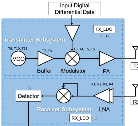
5.5.2                    Polarization radiation pattern . . . . . . . . . . . . . . . . . . . . . . . . . . . . . . . . . . . . . . . . . . 40
                      5.5.3                    Total power radiation pattern . . . . . . . . . . . . . . . . . . . . . . . . . . . . . . . . . . . . . . . . . . 41
6   Beam-steering Measurements . . . . . . . . . . . . . . . . . . . . . . . . . . . . . . . . . . . . . . . . . . . . . . . . . . . . . . . . . . . . . . . . . . .                                      42
    6.1  Beam-book Generation . . . . . . . . . . . . . . . . . . . . . . . . . . . . . . . . . . . . . . . . . . . . . . . . . . . . . . . . . . . . . . . . . .                                         42
    6.2  60 GHz Stacked Patches Antenna Array . . . . . . . . . . . . . . . . . . . . . . . . . . . . . . . . . . . . . .                                                                                 43
    6.3  Connected Slots Antenna Array Feeding a High Gain Lens at
         60 GHz . . . . . . . . . . . . . . . . . . . . . . . . . . . . . . . . . . . . . . . . . . . . . . . . . . . . . . . . . . . . . . . . . . . . . . . . . . . . . . . . . . . . . . . . . . . .   45
    6.4  Dipole Antenna Array . . . . . . . . . . . . . . . . . . . . . . . . . . . . . . . . . . . . . . . . . . . . . . . . . . . . . . . . . . . . . . . . . . . .                                     47
         6.4.1    Linear polarized dipole array . . . . . . . . . . . . . . . . . . . . . . . . . . . . . . . . . . . . . . . . . .                                                                       47
         6.4.2    Circular polarized crossed dipole array . . . . . . . . . . . . . . . . . . . . . . . . .                                                                                               48
7   Measurements in Radiation Hard Environment . . . . . . . . . . . . . . . . . . . . . . . . . . . . . . . . . . . . . .                                                                                51
    7.1  Irradiation Damages in Silicon . . . . . . . . . . . . . . . . . . . . . . . . . . . . . . . . . . . . . . . . . . . . . . . . . . . . . .                                                       51
         7.1.1     Total ionization dose and ionization damages . . . . . . . . . . . . . . .                                                                                                             52
    7.2  Transceiver Chip Under Investigation . . . . . . . . . . . . . . . . . . . . . . . . . . . . . . . . . . . . . . . . . .                                                                         53
    7.3  Proton Irradiation at Turku . . . . . . . . . . . . . . . . . . . . . . . . . . . . . . . . . . . . . . . . . . . . . . . . . . . . . . . . . . . .                                              53
    7.4  Electron Irradiation at CLEAR, CERN . . . . . . . . . . . . . . . . . . . . . . . . . . . . . . . . . . . . . . . .                                                                              55
8   Summary                      ....................................................................................................                                                                     57
Sammanfattning på Svenska                                                 ...........................................................................                                                     59
Acknowledgements                                  ..........................................................................................                                                              61
References                ........................................................................................................                                                                        63
1. Introduction
1.1 Motivation
Internet data demand is rapidly increasing globally due to a number of factors
including increased internet access, grown number of mobile phone users and
services, realization of Internet of Things (IoT), high-definition (HD) video
streaming, video calling etc. [1–3]. This increase in the demand is directly
linked with the technology enhancement that can assure the availability of
above mentioned services. As most of the services ask for immediate wireless
data, it is very challenging to meet these requirements without considering
additional high frequency bands, apart from the saturated sub-6 GHz bands
[4].
1.1.1 Millimeter-wave frequency bands
The license-free 60 GHz band (57–66 GHz) is one of the most suitable and
available options, which can help to cope with such high data demands. WiGig,
also known as 60 GHz WiFi, is meant for different services like audio/video
data transmission, display interfaces for HDTVs/monitors/projectors, wireless
local area networking (WLAN), fixed wireless access (FWA) and backhaul
communications etc. As shown in Fig. 1.1, the 57–66 GHz bandwidth is di-
vided into 4 channels where each channel has a bandwidth of 2.16 GHz. The
802.11ad standard defines the 60 GHz WLAN standard which not only sup-
ports up to 8 Gbps throughput but also ensures the seamless transition between
the existing WiFi bands (2.4 GHz and 5 GHz) and 60 GHz band [5].
Moreover, as shown in Fig. 1.2, the 3rd generation partnership project
(3GPP) has specified n258 (24.25 – 27.50 GHz) and n257 (26.50 – 29.50 GHz)
frequency bands for 5G communications. These bands, which are also called
26 GHz and 28 GHz respectively, intend to provide high data rate services for
Fig. 1.1. Four 60 GHz channels each of 2.16 GHz bandwidth.
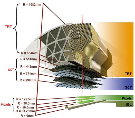
11Fig. 1.2. Frequency bands 26 GHz (n258) and 28 GHz (n257). short distances in high user density area, such as train/metro stations, densely populated areas, city centers, gathering places etc. Besides, homes and busi- nesses with FWA, IoT, 4K and 8K video streaming, industrial automation with low latency and high reliability are some other potential applications [6]. 1.1.2 Millimeter-wave links for tracker data read-out at CERN The upgrade of accelerators and experiments at the Large Hadron Collider (LHC) for high luminosity will result in multiple times higher event (collision) rates, which demands high data rate readout systems [7]. For instance, the readout data requirements at the upgraded ATLAS silicon microstrip tracker will be from 50 to 100 Tbps [8,9]. The availability of unlicensed 9 GHz band- width at 60 GHz (57–66 GHz) can fulfil this demand, as a single link can achieve multi-Gbps. However, wireless data transmission using millimeter- wave technology has not yet been used in trackers for particle physics exper- iments. The Wireless Allowing Data and Power Transmission (WADAPT) proposal [10] was formed to study the feasibility of wireless technologies in High Energy Physics (HEP) experiments at the European organization for nu- clear research (CERN). The objective is to provide a common platform for research and development in order to optimize the effectiveness and cost, with the aim of designing and testing wireless demonstrators for large instrumenta- tion systems. A strong motivation for using wireless data transmission is the absence of wires and connectors which will be an advantage in areas with low mate- rial budget and will also reduce the passive material. This passive material degrades the tracker performance through scattering and particle conversion. Besides, wireless transmission allows radial readout through the layers shown in Fig. 1.3 (a) which opens for topological readout of tracking data instead of current axial wired links shown in Fig. 1.3 (b). This topological readout of the tracking data can also reduce the on-detector data volume using inter-layer communications, and will drastically reduce the readout time and latency [12]. 1.1.3 Beam-steering High gain antennas and antenna arrays are required to achieve high through- put, which results in a narrow beam coverage, as beamwidth is inversely pro- 12
(a)                                       (b)
Fig. 1.3. ATLAS inner detectors [11] (a) Layered view of inner detectors (b) Pixel
detector showing significant cables contribution in active detector volume.

portional to the gain of an antenna array. In order to increase the coverage
and provide point-to-multipoint high data rate connectivity, beam-steering is
essential at millimeter-wave bands. The front-end system can provide spe-
cific weights (phases and amplitudes) to the individual antenna elements in
the array to steer the beam in a desired direction. As shown in Fig. 1.4, beam-
steering focuses the electromagnetic power towards specific targets instead of
having the waves spread in all directions. This improves the spectral efficiency
(bit/s/Hz) through higher signal-to-noise ratio (SNR) which results in achiev-
ing higher data rates. Beam-steering also helps to overcome the interference
caused by obstacles during the transmission in real-time. Concerning back-
haul communications, beam-steering diminishes the need of having separate
antennas for every link through high capacity point-to-multipoint connectivity.
For wireless data readout at CERN, there will be thousands of closely spaced
wireless links where beam-steering can enhance communication robustness
through point-to-multipoint connectivity.

1.2 Thesis Objective
In this thesis, different broadband and high gain millimeter-wave antenna ar-
rays are realized to fulfil the data demands in different application scenarios.
The arrays are integrated with the front-end radio frequency integrated circuits
(RFIC) to steer the beam in a desired directions. The 5G antenna arrays at
28 GHz are designed for places with high user density as well as for customer
premises equipment (CPE) applications. To transport this high volume data to
the core network, a fixed wireless access (FWA) link demands the implemen-
tation of a broadband, high gain and steerable narrow-beam array. This thesis

                                                                               13
Fig. 1.4. High throughput connectivity with multiple devices through beam-steering. presents the 60 GHz antenna arrays that satisfy these conditions and they can be used for both FWA as well as backhaul communications. At 60 GHz, a printed circuit board (PCB) antenna array integrated with the front-end RFIC is presented in Paper I and IV, whereas a broadband connected slots array feeding a high gain lens is designed in Paper III. To address the end user high data rate requirements, two antenna arrays are real- ized at 28 GHz. Instead of using a low-loss RF PCB, Paper V and Paper VI present the compact phased antenna arrays realized in the fan-out embedded wafer level ball grid array (eWLB) package. In comparison with the PCB an- tenna arrays, this antenna in package (AiP) solution is not only cost effective but it also reduces the interconnection losses. Moreover, for high data rate readout links at CERN, the key requirement are the components that can tolerate this radiation hard environment. As a first step towards this realization, a 17 MeV proton irradiation experiment is carried out at Åbu, Finland and Paper II presents the irradiation effects on a 60 GHz front-end transceiver chip. Besides, this thesis also presents a 200 MeV elec- tron irradiation of the chip, performed at CLEAR, CERN. 1.3 Thesis Organization The thesis is organized as follows: Chapter 2 discusses the wave propaga- tion along with losses and challenges for different environments. Chapter 3 presents individual elements used as building blocks for different arrays pre- sented in Chapter 4. The measurement methods used in this doctoral thesis are presented in Chapter 5, while Chapter 6 discusses the the beam-steering radiation pattern results. And at the end, proton and electron irradiation effects on the 60 GHz front-end transceiver chip are briefly discussed in Chapter 7. 14
2. Wave Propagation

The availability of larger bandwidths at millimeter-waves comes with the chal-
lenges like increased free space path loss, higher atmospheric absorption, scat-
tering, etc. These factors are further discussed in this chapter.

2.1 Free Space Propagation
The free space path loss is the major loss factor in mm-wave propagation. For
electromagnetic waves propagating in free space, the power received by an
antenna reduces four times (6 dB) as the distance between transmitting and
receiving antennas is doubled. For two isotropic antennas, wavelength and
distance dependence on the loss is given by the relation [13]:

                             Lfree space = (4πR/λ )2                         (2.1)
For loss in dBs:
                       Lfree space (dB) = 20 log10 (4πR/λ )                  (2.2)
where R is the line of sight (LOS) distance between two antennas and λ is
the free space wavelength at the operating frequency. As an example, the free
space path loss at 1 m distance for a 60 GHz link is 68 dB and for 5 GHz it is
46 dB. It is worth mentioning that this example is only true if the electrical size
of the antennas (in terms of wavelength) is same for both 60 GHz and 5 GHz
links, i.e., the free space path loss does not change with the frequency if the
physical area of the antenna remains constant [14]. The Friis transmission
equation gives more detailed relation by taking into account other transmit
and receive factors [15].
                                               λ2
                             Pr = Pt Gr Gt                                   (2.3)
                                             (4πR)2
where Pr and Pt are received and transmitted powers while Gr and Gt are gains
of receive and transmit antennas, respectively.

2.2 Atmospheric and Other Losses
Apart from the free space loss, there are also other factors which affect the mi-
crowave and millimeter-wave propagation. Some of these factors are gases in

                                                                                15
the atmosphere, rain, hydrometeors and micrometeors which not only absorb the electromagnetic energy but also cause the waves to scatter in un-desired directions. It can be Rayleigh scattering which occurs if the particles’ diame- ter is less than about one-tenth of propagating wavelength, or Mie scattering when particle diameter is larger than the wavelength [16]. The attenuation of electromagnetic energy due to absorption by water vapours and oxygen is presented in Fig. 2.1 [17]. For frequencies below 100 GHz, water vapour ab- sorption has a peak at 24 GHz while attenuation due to oxygen absorption is 10-15 dB/km around 60 GHz. Besides, the loss due to reflection and diffraction mainly depends upon the material and the surface on which the waves strike. On one hand, reflection and diffraction reduce the propagation range of millimeter-waves, but on the other hand, these factors also facilitate non-line-of-sight (NLOS) communica- tion [14]. Fig. 2.1. Attenuation at mm-wave due to water vapours and oxygen absorptions. 2.3 Wave Propagation in Trackers at CERN The trackers at CERN are flushed with dry nitrogen (N2 ), hence oxygen ab- sorption of 60 GHz waves is not a problem for high energy physics appli- cations. Besides, higher attenuation at 60 GHz allows for spatial frequency re-use in more compact regions. This makes 60 GHz a good candidate for inter-layer communications at CERN detectors, as the link distances are in tens of centimeters. Fig. 2.2 shows the proposed wireless links on the track- ers to replace the existing wired connections. It can be realized that even if 16
Fig. 2.2. Proposed 60 GHz wireless links for total/partial replacement of cables. The
green lines are silicon detector modules placed on co-axial cylindrical layers.

the cross-talk between layers is expected to be small, the interference between
links on the same layer can be a challenge. This effect can probably be moder-
ated by using high gain directional antennas and utilizing absorbing materials
between links, besides studies have shown that antennas can be placed as close
as 10 cm apart [8]. By exploiting polarization, the density of the links can be
further increased.

                                                                                  17
3. Antenna Elements: Building Blocks for Phased Arrays This chapter presents different antenna elements, e.g., microstrip patch an- tenna, dipole antenna and slot antenna, which are further used for designing antenna arrays for beam-steering applications. One common factor between above mentioned elements is their planarity which provides ease of integration with front-end radio frequency integrated circuit (RFIC). 3.1 Microstrip Patch Antenna First introduction of microstrip patch antennas can be traced back to 1950’s [18] though it gained more attention in 1970’s after the development of printed circuit board (PCB) technology. The microstrip patch antenna is a very com- mon type of antennas and is used for a wide variety of applications because of their advantages: compactness, planar configuration, cost effectiveness, sim- ple fabrication and ease of integration with RFIC. However, they are low gain antennas and inherently narrow banded, as their length (L) determines the resonance frequency (see Fig. 3.1). The impedance bandwidth of the patch antenna can be increased by using a thick substrate, but this gives rise to in- creased surface waves inside the substrate and thus more losses. The power coupled to these surface waves not only results in reduced radiation efficiency of the antenna but also increases the mutual coupling between elements in an antenna array. Another method to increase the bandwidth is by using low relative permittivity (εr ) substrates. This can be explained by the fact that in- creasing εr reduces the size of element (as ’L’ depends upon εr ) which in turn increases the quality factor (Q) of the resonator, thus making it more narrow- band [19]. For millimeter-wave applications, another challenge namely fabrication tol- erances become very important. As all the design dimensions are directly pro- portional to the wavelength, thus the lengths and widths reduce significantly at millimeter-waves frequencies. The widths of the feed transmission lines typically become very thin, around 1/10th of a millimeter, imposing serious fabrication tolerances and thus the fabrication cost can rise significantly as such tolerances can only be met with more expensive fabrication equipment. Different methods like transmission line model, cavity model or full-wave analysis [20–23] can be used to analyse the microstrip patch antennas. Based 18
on the transmission-line model, a set of design guidelines are outlined in this
section. These guidelines can lead to a first iteration of the patch element that
can be further optimized [24, 25].

                                          (a)

                                          (b)

                                                (c)
Fig. 3.1. Microstrip patch antenna (a) overall view (b) cross-sectional view of the
patch showing the fringing fields (c) effective length of the patch extended along radi-
ating edges.

3.1.1 Design principles
As shown in the Fig. 3.1 (a), a microstrip patch antenna has two radiating
edges acting as radiating slots. The resonant frequency of the microstrip patch
antenna depends upon its length L and the relation for the dominant mode
TM010 is given by

                                                                                    19
c
f= √ (3.1)
2L εr
where c is the speed of light in free space and εr is the relative permittivity of
the substrate.
Looking at the cross-sectional view in Fig. 3.1 (b), the fields extend away
from the edges of the patch, called fringing fields, which is the function of L/h
(h is the height of substrate) and εr . Moreover, the fields are not completely
confined within the substrate but some lines also exist in the air (in case of
dielectric-air interfaces). As the waves are present both in substrate and air,
an effective dielectric constant (εreff ) is introduced to account for fringing and
make the medium look homogeneous. Value of εreff can be anywhere between
1 and εr depending upon the relative permittivity of the substrate and W /h
ratio.
εr + 1 εr − 1 h
εreff = + [1 + 12 ]−1/2 (3.2)
2 2 W
where W is the width of the patch. As both L and W are unknown at this stage,
one can begin by using the below relation for width
c 2
W= (3.3)
2 f εr + 1
Because of the fringing fields, effective length Leff of the patch is somewhat
larger than the physical length L as shown in Fig. 3.1 (c),
Leff = L + 2ΔL (3.4)
where ΔL can be calculated using the equation below:
(εreff + 0.3)(W /h + 0.264)
ΔL = 0.412h (3.5)
(εreff − 0.258)(W /h + 0.8)
Including the above mentioned fringing field effects in Eq. 3.1, it will be-
come
c
f= √ (3.6)
2Leff εreff
The actual length of the patch can then be determined by evaluating
c
L= √ − 2ΔL (3.7)
2 f εreff
As mentioned earlier, the above equations shall give approximate dimen-
sions, which can then be optimized using electromagnetic simulation soft-
wares.
203.2 Stacked Patches Antenna
Another method to increase the bandwidth of a narrow-band patch antenna
is to introduce more than one closely spaced resonant structures. The elec-
tromagnetic coupling between stacked multi-layer patches shows a broad-
band impedance bandwidth and increased gain performance of the patch an-
tenna [26–29]. This antenna can be designed using a stacked patch structure
where one patch can be fed through probe or microstrip line while the other
patch is electromagnetically coupled. The closely spaced resonances make the
antenna broadband. The patches can be of rectangular or circular shapes. Fig.
3.2 (a) and (b) shows a stacked patches structure where the rectangular patch
is fed through a microstrip line on M2 metallic layer while the circular patch
is placed on M1 layer.
(a)
(b)
Fig. 3.2. Different views of stacked patches where rectangular patch is fed through
microstrip line and circular patch is fed through proximity effects. (a) Cross-sectional
view. (b) Layered view.
The stacked patches structure is defined by a number of dimensions, like
height of the substrates, lengths, widths and diameters of bottom and top
patches. These dimensions can be varied to get optimized values. Fig. 3.3
shows reflection coefficient (S11) graph for different parasitic patch diame-
ter (ppd) values of the top circular patch, while keeping the other dimensions
constant. The two resonances are very obvious in the graphs. These closely
spaced resonances result in the < –10 dB impedance bandwidth of more than
20 %. Similar results are obtained when length of the rectangular patch on the
bottom is varied. These stacked elements are used to design different series
and parallel antenna arrays which are further discussed in the next chapter.
21Fig. 3.3. S11 for different values of the parasitic patch diameter (ppd).
3.3 Dipole Antenna
Dipole antenna is a widely used antenna which most commonly consists of
two quarter-wave long legs as shown in Fig. 3.4 (a). The current (blue curve)
is zero while voltage (red curve) is maximum at the edges for a half wave long
dipole.
(a) (b)
Fig. 3.4. (a) A half wave dipole antenna consisting of two quarter wavelength long
legs. (b) E- and H-plane radiation pattern of the dipole.
The input impedance of the dipole is real when the dipole length is close
to half wavelength, which makes it a resonant antenna. This antenna can be
realized with the help of wires, metallic rods or metallic patches on the PCB.
Besides, unlike a patch antenna, the dipole antenna does not require a ground
plane as both of its legs are fed 180° out of phase. Fig. 3.4 (b) shows the E-
and H-plane radiation pattern for a half-wave dipole antenna. The radiation is
omni-directional in the H-plane and has two lobes in the E-plane. In 3D, this
pattern looks like a doughnut.
223.4 Slot Antenna
Slot antenna is a type of aperture antenna where an opening is made in a
metallic sheet. The energy radiates when a high frequency field exists on the
conducting plane around a narrow slot. According to Babinet’s principle, a
slot antenna is a complementary structure to a dipole antenna as shown in Fig.
3.5. This means that the polarization, current and voltage distribution around
the slot are complementary to that of the dipole antenna. As an example, if a
dipole antenna is placed vertically, it will have vertical polarization while if a
slot antenna is placed vertically it will have horizontal polarization. Besides,
the radiation pattern for a slot antenna is similar to that of a dipole antenna.
Fig. 3.5. A half wave slot antenna fed in the center.
234. Antenna Arrays for Beam-steering Applications This chapter briefly explains the design and fabrication of different antenna arrays presented in the thesis. Before proceeding to the design of antenna arrays, it is important to have a look at the array factor, which explains how arrays behave compared to a single stand-alone element. 4.1 Array Factor The antenna elements are placed at a specific distance from each other to create an antenna array. Each element can be fed in a way to direct the antenna array towards a specific direction. The proper selection of weights (amplitude and phase) to the individual elements in the array can increase the energy in one direction while canceling out the signals from undesired directions. The combination of antenna element radiation pattern and its position in the antenna array defines the array factor. As the name suggests, the array factor has great importance in the array theory. Fig. 4.1. A linear array having equally spaced N number of elements and with a signal is being received at an angle θ to the array normal. A linear phased array is shown in Fig. 4.1 where the elements are spaced by a distance p from each other with a plane wave received at an angle θ with respect to the array normal. Due to the reciprocity theorem, the same 24
results apply for the transmit mode. As the wave can have both time and space
dependence, the phase is expressed as
                                     2π
                           φ = ωt ±     l = ωt ± kl                      (4.1)
                                      λ
where k = 2π λ is the wave number. The received signal will travel a distance
p sinθ from the element number N to element N − 1, and likewise 2p sinθ to
N − 2. If we neglect the time dependence term in the receive signal, phase of
the signal received by the ith element will be
                             φi = k0 (N − i) p sinθ                         (4.2)
for i = 1, 2, ...., N − 1, N and where k0 is the free space wave number.
   If Re (θ ) is the radiation pattern of individual element, then the signal re-
ceived by the ith element will be

                       Ri (θ ) = Re (θ ) Ai e jk0 (N−i)   p sinθ
                                                                            (4.3)
   where Ai is the amplitude of the signal received by ith element. Then the
total power received by the array can be written as a summation:
                                             N
                                R(θ ) = ∑ Ri (θ )                           (4.4)
                                           i=1
  expansion gives
                                       N
                      R(θ ) = Re (θ ) ∑ Ai e jk0 (N−i)     p sinθ
                                                                            (4.5)
                                       i=1
   Thus, the total radiation pattern of an antenna array is the pattern multi-
plication of two terms, individual element pattern [Re (θ )] and a summation
term. This multiplication tells that in order for an array to have a wide-angle
beam-steering, the individual element should have a wide beam radiation pat-
tern [30–34]. The summation term in Eq. 4.5 is called the array factor and is
defined as the radiation pattern of an array having N isotropic elements [35].
                                                 N
                  Array Factor = AF = ∑ Ai e jk0 (N−i)             p sinθ
                                                                            (4.6)
                                             i=1
  The array factor is thus the function of weights to the individual elements
and spacing between them.

4.2 Stacked Patches Antenna Array
This section briefly discusses the design of the stacked microstrip antenna ar-
ray presented in paper I. The aim is to design an array having less than – 10 dB

                                                                              25
impedance bandwidth as well as the 3 dB gain bandwidth covering the com- plete 60 GHz license free band 57–66 GHz with wide-angle beam-steering. Moreover, the array needs to be compact and planar as it will be integrated with a front-end radio frequency integrated circuit (RFIC) [36]. Keeping above mentioned requirements in view, the microstrip patch antenna elements are selected after investigating different antenna elements. A choice is made based on their compactness and ease of integration with the RFIC. Besides, wide beamwidth of the patch antenna can help to achieve wide-angle beam- steering [37]. This antenna however lacks in impedance bandwidth because of its resonant structure. As discussed in Section 3.2, this limitation is overcome by using stacked patches which improves the impedance bandwidth. Different multi-layer structures working at 60 GHz are realized using low temperature co-fired ceramics (LTCC) [38–41]. The LTCC provides flexibility in realizing arbitrary number of layers, cross layer VIAs and open and embedded cavi- ties. However, it has a disadvantage of relatively higher cost compared with a printed circuit board (PCB) process [42]. The PCB implementation has been used in [29] to realize 5-metal layers differential phased array antenna at 60 GHz. Likewise, a 4-metal layers, microstrip line fed, aperture coupled multi- layer antenna array is presented in [43]. In the present work, we have used 3-metal layers (one ground layer and two layers with stacked patches) to de- sign the antenna array, besides, a low εr material is used in the design as high εr increases the Q factor and makes the patch more narrow-band [19]. Fig. 4.2. 60 GHz RFIC integrated with 16 × element RX stacked patch antenna array. Same can be repeated on the TX side. The idea of integrating the RFIC with the antenna array is presented in Fig. 4.2 where the RFIC is feeding 16 × columns of a single element stacked patch antenna at the RX side. The TX side will look similar. As the array has 16 × columns in the azimuth (H) plane, it will result in a narrow directive beam. However, having a single patch in the elevation (E) plane produces a wider beamwidth, so different options are investigated to reduce this beamwidth. 26
Fig. 4.3. Beam squint as a function of frequency for series fed antenna array.

    A series array is more compact and does not create any space problems
when 16 × columns are placed side-by-side. However, radiation beam of a
series array squints as a function of frequency. This is because the elements of
the array are fed with different phases when moving from 57 to 66 GHz. As
shown in Fig. 4.3, the array designed for 61.5 GHz center frequency radiates
in the desired broadside direction. However for frequencies lower and higher
than the center frequency, the phases at the input of each patch are either pro-
gressively increasing or decreasing, which makes the beam shift away from the
broadside. The farther is the frequency of operation from 61.5 GHz, the higher
is this beam squint. The beam squint could be useful for certain applications,
e.g., radar communication, but is not desired for broadband communications.
    It is further analysed that the beam squint gets worst for series arrays having
more than two number of elements. So, instead of using a 4-element series
array, a 4-element centrally fed series array is designed which keeps the beam
squint to an acceptable level as well as decreases the elevation plane beam-
width. Fig. 4.4 (a) shows the single element stacked patches antennas which
are used as building block for the other arrays. Both elements use rectangular
patches as the feeding patch while parasitic patch is circular in one case and
rectangular in the other case. The same structure of stacked patches is repeated
to design 2-element series arrays, 4-element centrally fed series arrays and
4-element compact corporate array shown in Fig. 4.4 (b), (c), (d) and (e)
respectively. The 2-element array on the left (circular patch over rectangular)
is integrated with the 60 GHz RFIC [36] and the beam-steering results with
the EIRP are presented in papers I and IV.

                                                                                27
(a)
(b)
(c)
(d)
(e)
Fig. 4.4. Top view of the stacked patches antenna elements and arrays (a) Single ele-
ment antennas (b) 2-element series fed antenna array (c) 4-element centrally fed series
array with circular patches on top of rectangular patches (d) 4-element centrally fed
series array with rectangular patches both on top and bottom (e) Compact 4-element
corporate fed array with circular patches on top of rectangular ones.
284.3 Connected Slots Antenna Array (CSAA) Feeding
High Gain Lens at 60 GHz
This section presents a high gain 60 GHz beam-steered antenna array designed
mainly for mobile backhaul communications where all nodes are at the same
height, so the elevation plane will have a fixed narrow-beam whereas the beam
will be steered in the azimuth plane. The feed-switchable antenna arrays feed-
ing the lens have been largely reported in the literature [44–48], however, the
beam can only be steered to the predefined angles with this technique, and
the link can break if the orientation of antenna changes from its predefined
position. This is true especially if we talk about the narrow-beam backhaul
communications. Instead this work proposes a linear phased antenna array to
feed a dielectric lens antenna, where the feed will not only have significantly
higher gain compared to the single element used in feed-switching, but will
also allow to steer the beam to any arbitrary angle in ±45◦ range with the help
of front-end RFIC. Moreover, excitation of 16-paths at the same time results
in spacial power combining and will increase the effective isotropic radiated
power (EIRP) by 12 dB compared to single element excitation, as doubling
the number of excitations results in a 3 dB rise.
The connected slots PCB array presented in Fig. 4.5 (a) will feed the lens
shown in Fig. 4.5 (b) and (c). For characterization of the prototype, a 1:16
power splitter is designed to feed the connected slots array at sixteen equidis-
tant points. This linear array extends along the y-axis, which will act as a
point source in the elevation plane as can be seen in panel (b) of the figure.
The lens thus plays major role in this plane to reduce the beamwidth. Besides,
as connected slots array is extended along LLens in the azimuth plane [shown
in panel (c) of Fig. 4.5], the beam will be steered in this plane with the help of
RFIC. However, for performance verification, three different power splitters,
shown in Fig. 4.6, are designed to steer the beam at 15°, 30° and 45° apart
from the power splitter shown in Fig. 4.5 (a) which corresponds to broadside
radiation (0°).
When all 16 feed points on the connected slots antenna array (CSAA) are
excited in phase (0◦ beam), it is mainly the array itself which produces a 10◦
HPBW in the azimuth plane and the lens has no contribution in it. However,
when the CSAA is excited to steer the beam away from the broadside in the
azimuth plane, the hemispherical terminations of the lens play their role to
enhance the gain. For usual phased arrays, the gain reduces with higher beam-
steering angles because of angular dependence of element radiation pattern,
called scan loss [49]. However, in our case, the gain increases up to certain
beam-steering angles because of hemispherical terminations of the lens. Paper
III contains further details in the Fabrication and Measurement section.
29(a)
(b)
(c)
Fig. 4.5. Design view of dielectric lens (a) Elevation plane (XZ) view (b) Azimuth
plane (YZ) view of the lens antenna, the CSAA extend along Y-axis.
(a) (b) (c)
Fig. 4.6. Power splitters to steer the beam at (a) 15◦ (b) 30◦ (c) 45◦ .
304.4 Dipole Antenna Arrays: 28 GHz Antenna in
Package (AiP)
The good performance PCB antenna arrays not only demand for low loss
costly substrates, but also cause more integration losses with RFIC because of
increased transmission line lengths and transitions from chip to the antenna.
Moving from sub-6 GHz bands to millimeter wave bands makes the antennas
more compact as physical dimensions are directly proportional to the opera-
tional wavelength. This allows to design antennas and antenna arrays directly
in the RFIC package, which not only reduces the additional PCB cost but also
reduces the interconnect lengths. This section discusses the design of two sep-
arate antenna arrays, a linear polarized dipole array and a circular polarized
crossed dipole array, both working at 28 GHz for high data rate applications.
4.4.1 RFIC package
The smallest chip package that is of the same size as the chip is called fan-
in wafer level package (FIWLP) shown in Fig. 4.7 (a). In the traditional
assembling process, individual dies are packaged after dicing them from a
wafer, while in FIWLP technology the integrated circuit (IC) is packaged at the
wafer level by using the wafer fabrication processes and tools [50]. As this is a
true chip scale package (CSP), the package allows only for limited number of
interconnect solder bumps for DC and high frequency signals. In comparison,
panel (b) of the figure presents an enhanced version of standard wafer level
package, called fan-out wafer level package (FOWLP). The fan-out region
in the FOWLP not only allows for more interconnect bumps for connectivity
between chip and PCB but it also allows to place antennas / antenna arrays on
re-distribution layer (RDL) in this region.
Different fan-out antenna designs have been presented in [51–63] at mil-
limeter waves. Most of the designs presented in the above reference list are
realized by using either multiple RDLs, double mold, through mold VIAs,
or with an airgap in the mold. These variations increase complexity of the
package, thus making it cost-ineffective.
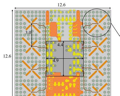
The 28 GHz RFIC package used in this work is presented in Fig. 4.8. The
0.5 mm ball-grid array (BGA) package comprises of a single mold layer, three
passivation (PSV) layers (PSV1, PSV2 and PSV3) and two RDLs (RDL1 and
RDL2) [64]. The dummy solder bumps under the fan-out region are required
for mechanical stability of the package. Presence of these dummy balls in the
fan-out region has been investigated by simulating a microstrip patch antenna
with and without the solder balls in the substrate. Adding these balls in the
substrate results in slight increase in the dielectric constant which has been
taken into account while designing the antenna array. This embedded wafer
level BGA (eWLB) package has 12.6×12.6 mm2 dimension while the die
31(a)
(b)
Fig. 4.7. Cross-sectional view of the wafer level packages (WLP) (a) fan-in WLP (b)
fan-out WLP.
covers around 4.5×4.5 mm2 . This leaves with 12.6×4.05 mm2 space on each
side of the die to design the antenna arrays.
Fig. 4.8. Cross-section of the fan-out WLP used in the project, containing three
passivation (PSV) and two re-distribution layers (RDL).
4.4.2 Linear polarized dipole array
Placement of different antenna elements in the fan-out region has been investi-
gated, which suggests the use of a dipole antenna because of space constraints
and wide beamwidth in the H-plane. As shown in Fig. 4.9, both TX and RX
antenna arrays are identical and comprise of four dipole elements, placed at
RDL1 in the embedded wafer level ball grid array (eWLB) package. The mu-
tual coupling between the elements is significantly reduced with the help of a
narrow metallic strip placed on RDL2 in the middle of every two dipole ele-
ments. Fig. 4.10 shows the mutual coupling between two neighboring dipole
legs. It can be seen that the difference is around 5 dB in the shown frequency
band and this reduction in mutual coupling significantly helps to improve the
impedance bandwidth of the array.
32Fig. 4.9. TX and RX antenna arrays placed at RDL1 in the fan-out area of the 12.6 ×
12.6 mm2 package. The inset shows the zoom-in view.
The intended direction of radiation is through the mold, so to suppress the
back lobe radiations, localized reflectors are placed at quarter wavelength dis-
tance from the antenna array in the FR-4 PCB, as shown in Fig. 4.11. More-
over, to suppress the surface wave propagation inside FR-4, a rectangular cav-
ity is introduced with the help of PCB VIAs.
Fig. 4.10. Mutual coupling between dipole legs with and without the narrow metalic
strip placed in the middle on RDL2.
Horn shaped heatsink
The presence of the heatsink cannot be neglected in the antenna array design
as it is a key requirement in cooling down the active chip. As the heatsink
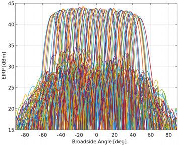
33needs to be attached with the chip, it stays in close proximity to the antenna array which affects the radiation performance of the array. So, it is necessary to take into account the presence of the heatsink while designing the antenna array and this could turn in a positive asset. In this work, the heatsink is shaped as a horn antenna shown in Fig. 4.11, which not only dissipates the heat from the chip but also improve the radiation performance of the antenna arrays. Fig. 4.11. An aluminium heatsink placed on top of the chip package. Reflector backed cavities are also shown in the FR-4 PCB. 4.4.3 Circular polarized crossed dipole array Apart from the linear polarized array, a circular polarized antenna array is designed in the package for 28 GHz 5G applications. A crossed dipole is well known for its circular polarization and dual polarization characteristics [65– 69]. Fig. 4.12 (a) presents the crossed dipole antenna arrays in the package and the zoom-in view shows the dipoles are fed through planar differential pairs coming from the chip pads. The lengths of the two dipoles in a crossed dipole are kept different from each other as suggested in [69] and this difference is further optimized to get the axial ratio less than 3 dB. Moreover, to get the directional coverage towards the broadside direction and suppress the back radiation, a reflector layer is introduced in the PCB at a quarter-wave distance from the dipole array as shown in Fig. 4.12 (b). A half-cylindrical aluminium heatsink is placed on top of the die for heat dissipation. 34
(a)

                                         (b)
Fig. 4.12. Package layout. (a) RX and TX antenna arrays are designed on left and right
to the chip, respectively. The inset shows the zoom-in view of the antenna element.
All the dimensions are in mm. (b) cross-sectional view of the package integrated with
the FR-4 PCB and a heatsink placed on top of the die.

                                                                                   35
5. Measurement Methods
5.1 Reflection Coefficient
The reflection coefficient defines how much power is reflected back due to
impedance mismatching in the transmission path. Equation 5.1 defines the
reflection coefficient (Γ) in terms of load and characteristic impedance.
ZL − Z0
Γ= (5.1)
ZL + Z0
where ZL is load impedance and Z0 is characteristic impedance. If load and
characteristic impedance are matched (are the same), Γ = 0, i.e., no reflection
occurs and maximum power is transferred from source to load. When Γ is
expressed in terms of S-parameters, it is referred to as S11 .
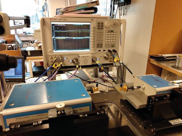
In this thesis, the Vector Network Analyzer (VNA) Keysight PNA N5225A
is used along with the millimeter wave OML extension modules [70] to mea-
sure the impedance matching of the antennas and antenna arrays. Fig. 5.1
shows the above mentioned network analyzer connected with the WR-15 (50
to 75 GHz) extenders. The measurements are carried out using coaxial port
as well as ground signal ground (GSG) probe after performing the one-port
short-open-load (SOL) calibration.
Fig. 5.1. Setup to measure the S-parameters.
365.2 Gain
Gain is an important characteristic in defining the performance of an antenna
that describes the maximum radiation in a certain direction in relation to an
isotropic antenna. The gain is usually presented in dBi where ’i’ stands for
isotropic. In this thesis, gain-transfer or gain-comparison method [24] is used
to measure the gain of antenna arrays. These measurements are carried out
with the help of the Keysight PNA N5225A along with millimeter wave OML
frequency extenders. Waveguide S21 calibration is performed on OML exten-
ders and the losses of the waveguide to coaxial transition and coaxial cable
are measured separately. These losses are then taken into account during post-
processing gain calculations. Three antennas are used in these measurements
as shown in Fig. 5.2, where the transmitting antenna can be of any type or gain,
while the receiver antenna is switched between standard gain horn and antenna
under test (AUT). Input power at the transmitter side should be the same for
both receivers and the system disturbances should be minimum when switch-
ing between the receiving antennas. The gain of AUT can then be calculated
by using the FRIIS equation:
GAUT = GS + PAUT − PS (5.2)
where, GAUT is the gain of AUT, GS is the gain of standard horn antenna,
PAUT is power received by AUT and PS is the power received by standard horn
antenna. All values are in dB.
Fig. 5.2. Setup to measure the gain using gain comparison method. TX is on the left
while RX on the right.
5.3 Radiation Pattern
In 2D radiation patterns, azimuth and elevation plane measurements are the
most common representations of an antenna. Two different methods are used
in this work to measure the radiation pattern, 1) rotate the AUT around its
center when the standard antenna remains stationary [Fig. 5.3 (a)] 2) rotate
37the standard horn antenna around the stationary AUT [Fig. 5.3 (c)]. When
measuring the far-field radiation patterns, the second method is feasible for
millimeter and sub-millimeter wave measurements where the far-field distance
to the antenna is not very high. The physical setup for the aforementioned
methods is shown in Fig. 5.3 (b) and (d), respectively.
(a) (b)
(c) (d)
Fig. 5.3. Antenna radiation pattern measurement setup. (a) AUT is rotated in azimuth
and elevation plane so the distance from the standard antenna remains constant. (b)
Actual measurement setup for schematic shown in (a). (c) AUT is stationary and
standard antenna is rotated in the azimuth and elevation plane around the AUT in
large circles in such a way that the distance to the AUT remains constant. (d) Actual
measurement setup for schematic shown in (c).
5.4 Polarization
The polarization of an electromagnetic (EM) wave is defined by the orienta-
tion of the E field component in the plane perpendicular to the direction of
propagation. As shown in Fig. 5.4 where z is the direction of wave propaga-
tion, the wave is said to be linear polarized if the E-field varies linearly [(as in
panel (a) of the figure]. The linear polarized wave could be horizontal, vertical
or oriented any other angle. Likewise, looking in the plane perpendicular to
38the direction of propagation, the wave is said to be circular or elliptical polar-
ized if the E vector-head makes a circle [as in Fig. 5.4 (b)] or ellipse [as in
Fig. 5.4 (c)] in that plane, respectively.
(a) (b) (c)
Fig. 5.4. Illustration of different polarizations. (a) Linear (b) Circular and (c) Elliptical
polarization.
5.5 Polarization Measurement
For a linear polarized antenna, two radiation patterns are of great interest;
co-polarization and cross-polarization patterns. As the name suggests, co-
polarization radiation pattern of a linear polarized antenna is measured by
placing AUT and standard antenna in a way that their E-field vector has the
same orientation. Whereas to measure the cross-polarization radiation pat-
tern, any one of the two antennas is rotated by 90°. The higher is the isolation
between co- and cross-polarization measured power levels, the better linear
polarized is the AUT.
5.5.1 Axial ratio measurement
Most practical circular polarized antennas are not purely circular but rather
elliptical polarized, having a major and a minor axis as shown in Fig. 5.4 (c).
The ratio of major to minor axis is called the axial ratio (AR) of the antenna.
The value of AR can be between 0 dB (for pure circular polarized antenna)
and ∞ (for pure linear polarized antenna).
The measurement setup for the AR of an antenna is shown in Fig. 5.5,
where the linear polarized (LP) antenna is rotated around its center in the plane
perpendicular to the direction of propagation, and power level is measured
at different steps during this rotation. As an example, for an AUT that is
broadside directed, Fig. 5.6 (a) shows the power levels measured at every 6
degrees in the above mentioned rotation, resulting in an ellipse. The axial ratio
and the orientation of major axis can be determined by the normalized polar
39You can also read