A 24 GHz Direct Conversion Receiver for FMCW Ranging Radar Based on Low Flicker Noise Mixer - MDPI
←
→
Page content transcription
If your browser does not render page correctly, please read the page content below
electronics
Article
A 24 GHz Direct Conversion Receiver for FMCW Ranging
Radar Based on Low Flicker Noise Mixer
Dongze Li 1,2 , Qingzhen Xia 1,2 , Jiawei Huang 1,2 , Jinwei Li 1,2 , Hudong Chang 1 , Bing Sun 1
and Honggang Liu 1, *

                                            1   High-Frequency High-Voltage Device and Integrated Circuits R & D Center, Institute of Microelectronics,
                                                Chinese Academy of Sciences, Beijing 100029, China; lidongze@ime.ac.cn (D.L.);
                                                xiaqingzhen@ime.ac.cn (Q.X.); huangjiawei@ime.ac.cn (J.H.); lijinwei18@mails.ucas.edu.cn (J.L.);
                                                changhudong@ime.ac.cn (H.C.); sunbing@ime.ac.cn (B.S.)
                                            2   School of Microelectronics, University of Chinese Academy of Sciences, Beijing 100029, China
                                            *   Correspondence: liuhonggang@ime.ac.cn; Tel.: +86-010-8299-5803

                                            Abstract: In this paper, a 24 GHz direct conversion receiver (DCR) for frequency-modulated
                                            continuous-wave (FMCW) ranging radar based on low flicker noise mixer in 90 nm silicon-on-
                                            insulator (SOI) CMOS technology is presented. A low-noise and low-power low-noise-amplifier
                                            (LNA) adopting simultaneous noise and input matching (SNIM) method is designed. Neutralized
                                            technology and boost inductor are introduced to improve performance. The measurement results of
                                            standalone LNA show that the peak gain is 17.2 dB at 23.8 GHz and the −3 dB bandwidth is around
                                            2.2 GHz from 22.8 GHz to 25 GHz. The LNA achieves an average 3 dB NF within the 24 GHz band.
                                            A current-bleeding mixer is used to lower noise and the factors influencing flicker noise have been

                                     discussed. Proper element values and local oscillator (LO) power have been chosen to make the mixer
                                            low-noise. Measurement results illustrate that the receiver exhibits 20.3 dB peak gain, 7 dB SSB noise
Citation: Li, D.; Xia, Q.; Huang, J.; Li,
                                            figure (NF) and −22 dBm IP1dB . Flicker noise of the mixer and the receiver are measured respectively
J.; Chang, H.; Sun, B.; Liu, H. A 24
GHz Direct Conversion Receiver for
                                            and the noise knee-point of receiver is observed 60 kHz. The receiver consumes only 16 mW with
FMCW Ranging Radar Based on Low             chip area of 0.65 mm2 including pads. The results demonstrate that the proposed receiver can be a
Flicker Noise Mixer. Electronics 2021,      promising candidate for FMCW ranging radar.
10, 722. https://doi.org/10.3390/
electronics10060722                         Keywords: receiver; 24 GHz; SOI; flicker noise; mixer; DCR; FMCW

Academic Editor: Egidio Ragonese

Received: 14 February 2021                  1. Introduction
Accepted: 15 March 2021
                                                 Since the Federal Communications Commission (FCC) granted unlicensed 24 GHz
Published: 18 March 2021
                                            band as Industrial Scientific Medical (ISM) band, intense research activity toward real-
                                            ization of highly integrated solutions around 24 GHz band is presently underway [1].
Publisher’s Note: MDPI stays neutral
                                            Advances in integrated circuit and semiconductor device technologies are now enabling
with regard to jurisdictional claims in
                                            the development of low-cost radar products for the automotive [2], industrial [3] and
published maps and institutional affil-
                                            consumer electronics [4]. Among them, the classical direct-conversion receiver has at-
iations.
                                            tracted wide-spread attention recently for its simple architecture and easy integration
                                            with the baseband circuit, as well as for its low power consumption and potentially low
                                            manufacturing costs [1].
                                                 A simplified block diagram of a DCR is illustrated in Figure 1. The echo signal is first
Copyright: © 2021 by the authors.
                                            picked up by a receiver antenna before being passed through a band select filter. The process
Licensee MDPI, Basel, Switzerland.
                                            is usually carried out in a printed circuit board (PCB). Afterwards, the signal is scaled up
This article is an open access article
                                            by a low-noise-amplifier (LNA) and is subsequently frequency down-converted by the
distributed under the terms and
                                            mixer with a LO signal produced by the voltage-controlled oscillator (VCO). The LNA and
conditions of the Creative Commons
Attribution (CC BY) license (https://
                                            mixer are key parts to complete the down-conversion operation and their performance
creativecommons.org/licenses/by/
                                            influence subsequent detection circuit block most. In this work, the designs mainly cover
4.0/).
                                            the implementation and optimization of the low noise amplification and subsequent

Electronics 2021, 10, 722. https://doi.org/10.3390/electronics10060722                                      https://www.mdpi.com/journal/electronics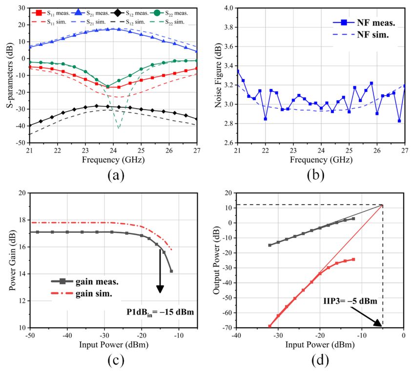
Electronics 2021, 10, 722                                                                                          2 of 12

                            frequency downconversion. Then, they are integrated into a low-power radar receiver
                            radio frequency (RF) front-end.

                            Figure 1. Simplified block diagram of DCR (direct conversion receiver).

                                  Nevertheless, the flicker noise is the biggest obstacle in pursing the DCR design.
                            In millimeter-wave radars, the FMCW type has drawn the most attention because of
                            its compact size and robustness over weather, temperature and light conditions [5–8].
                            However, when a DCR radar is used to measure the distance, the intermediate frequency
                            (IF) calculated from FMCW may lie in the high flicker noise area. As shown in Figure 2,
                            the useful baseband signal will be “buried” in noise, leading to poor measured result. A
                            low flicker noise receiver is attractive in DCR applications. Several publications mentioned
                            low flicker noise designs. Traditional current bleeding method was described in [9,10] and
                            in [11] a gm-boost method was introduced with an additional circuitry connected to the
                            switching pair transistor of the mixer to enhance gain. No measured results have been
                            reported on 24 GHz low flicker noise receiver. In this paper, an intuitive and understandable
                            current bleeding method is introduced to get relatively low flicker noise. Flicker noise of
                            the mixer and the receiver are measured respectively for the first time.

                            Figure 2. Baseband signal degraded by flicker noise.

                                 The SiGe technology was once the first choice due to its excellent-performance and
                            high-efficiency [2], but the low integration level and high cost are insufferable. In recent
                            years, the burgeoning CMOS technology has become a hotspot for low-cost mm-wave
                            radar chips [12] with its high integration and low cost. However, the lossy substrate
                            and low-Q-factor passive components, such as inductors and capacitors, make it hard to
                            achieve a high-gain, low-noise and low-power-consumption receiver. Compared with bulk
                            CMOS technology, the SOI’s buried oxide layer above low resistivity substrate decreases
                            RF coupling to the conductive silicon substrate [13]. Based on that, the SOI CMOS process
                            is promising to overcome the weakness mentioned above. By greatly improving the circuit
                            performance with limited increased cost, the SOI CMOS is expected to be cost-effective for
                            good performance, low cost radar chip.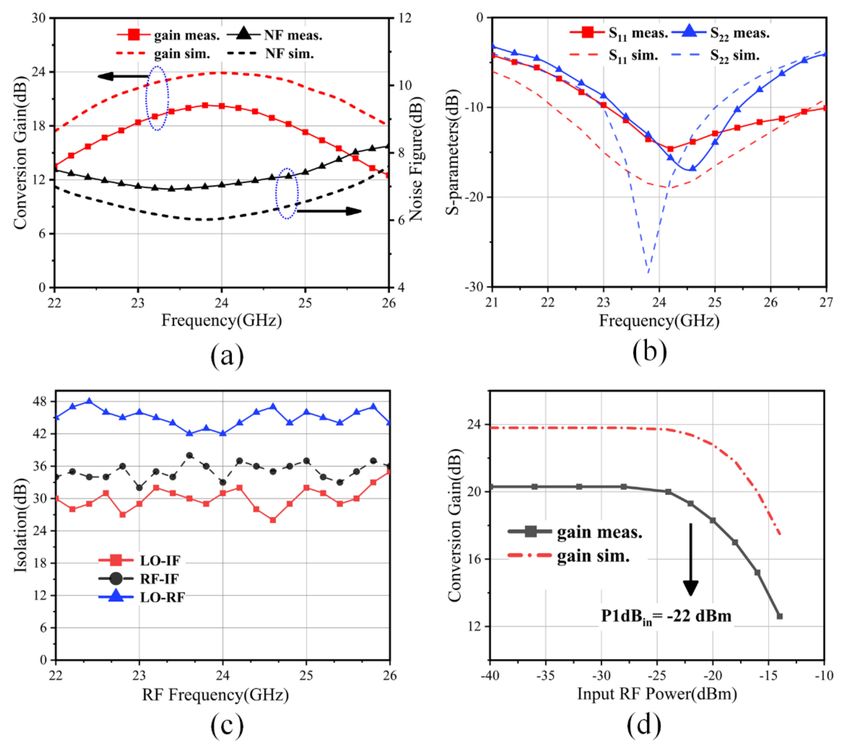
Electronics 2021, 10, 722                                                                                              3 of 12

                                 In this paper, a low noise receiver is proposed. The paper is organized as follows-in
                            Section 2, the FMCW principle is presented. In Section 3, the low noise receiver circuit
                            implication is described in detail. A low-noise and low-power LNA is proposed. The factors
                            influencing flicker noise of mixer are analyzed and a low flicker noise mixer is designed.
                            Measurement results and comparison with simulation results are shown in Section 4. Results
                            indicate that the proposed receiver promises for 24 GHz FMCW Ranging Radar.

                            2. FMCW Principle
                                 The principle of the FMCW ranging radar is discussed in detail here [14]. The fre-
                            quency of FMCW signal changes linearly with time. A simplified model of FMCW signal
                            can be seen in Figure 3. By calculating the frequency difference, the delay between the
                            transmitted wave and the reflected wave can be known to determine the position of the
                            target. It can be expressed as
                                                                           c· T · f r
                                                                       R=                                             (1)
                                                                              2B
                            where R stands for the distance between target and radar, c is the speed of light, T is the
                            duration of the chirp, f r is the beat frequency and B is the bandwidth of carrier frequency.

                            Figure 3. FMCW (frequency-modulated continuous-wave) principle of a sawtooth wave.

                                  As mentioned above, the beat frequency f r goes linearly with distance R. If the target
                            is relatively close to the radar, the R is small; thus, the beat frequency f r is also small,. For
                            example, when the distance between radar and target is 3 m, B is 250 MHz and T = 0.5 ms
                            is a regular resolution. Thus, the calculated 10 kHz beat frequency f r is lying in the high
                            flicker noise area exactly. As a consequence, the short-range detecting ability deteriorates.
                                  The beat frequency containing information of target is calculated from received RF
                            signal and LO signal and it is irrelevant to the received signal scope. In this way, the
                            receiver used for FMCW can loosen restriction of linearity.

                            3. Circuit Implementations
                                 Figure 4 shows the proposed direct down-conversion receiver with dimensions of the
                            RF active devices. The passive element values of proposed circuit are shown in Table 1.
                            These element values are based on the results of EM simulation. The receiver is based on
                            the zero IF architecture with RF and LO signals operating in the 24 GHz frequency band.
                            Low noise, low power consumption and high integration are some of the important system
                            requirements of the receiver. To avert lossy balun and reduce the power consumption
                            of this circuit, single-end topology is used. Ld2 was the load of LNA and its inductance
                            was chosen to form the matching circuit with Cp2 and Lp2 between the output of LNA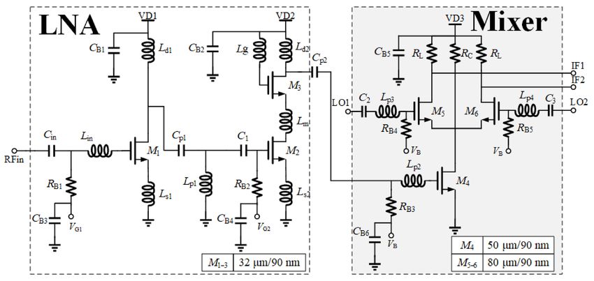
Electronics 2021, 10, 722                                                                                           4 of 12

                            and input of mixer. The LO input ports of the mixer were matched to 50 Ω impedance by
                            introducing the matching inductors Lp3 and Lp4 .

                                        Figure 4. Schematic of proposed receiver.

                            Table 1. Values of the circuit elements of the proposed receiver.

                               Cin        CB1–6       Cp1        Cp2        C1-3        Lin      Ls1      Ls2      Ld1
                              1.25 pF     2 pF       200 fF      550 fF     1 pF      720 pH    300 pH   270 pH   600 pH
                                Ld2        Lm          Lg         Lp1        Lp2       Lp3–4     RB1–5     RL       RC
                              450 pH     130 pH     150 pH      180 pH     300 pH     430 pH    1.2 kΩ    800 Ω    60 Ω

                                According to the system noise cascading formula, to keep the whole system low noise,
                            LNA as the first stage should have enough gain and low noise [15]. The mixer used for
                            down-converting RF signals should keep low flicker noise. Detailed design methods are
                            described in following parts.

                            3.1. LNA Design
                                  As depicted in Figure 4, a two-stage single-end LNA is designed in our work. The
                            first stage plays the key part in the noise figure of the system. To meet the requirements
                            of noise figure and gain, a common-source (CS) amplifier is set to be first stage to keep
                            the circuit low-noise, followed by a cascode amplifier to enhance gain. SNIM method [16]
                            was introduced in this design to ensure high gain and low NF without sacrificing each
                            other, which used to be a tradeoff. As shown in Figure 4, Ls1 and Ls2 worked as source
                            degeneration inductors to simplify the LNA’s input and noise matching. The researcher
                            in [13] reported that the SNIM state will be easily influenced by the bias circuit when
                            designing LNAs, leading to mismatch and deteriorated performance. Based on simulated
                            results, a 1200 Ω resistor was chosen in the bias circuit and the bias circuit was placed
                            proposition before Lin . The input port of the LNA is matched to 50 Ω impedance. In
                            receiver the output port of the LNA is matched to mixer and in standalone LNA the output
                            port of the LNA is matched to 50 Ω impedance.
                                  To reduce the power consumption as much as possible, bias voltage of amplificatory
                            transistors is elaborately set to 0.55 V for enough gain, acceptable NF and power consump-
                            tion. Moreover, sizes of transistors M1 , M2 and M3 were selected elaborately through
                            simulation. Lm , as neutralized inductor, was added between the CS and the common-gate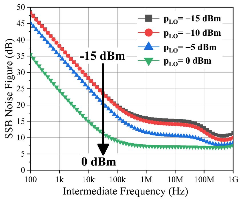
Electronics 2021, 10, 722                                                                                                    5 of 12

                                  (CG) transistors to resonate with parasitic capacitor to minimize the NF and increase the
                                  gain [15]. Meantime, an inductor Lg was added at the gate of the CG transistor as resonant
                                  tank to boost gain at the target frequency [17]. Lm was well-designed transmission line
                                  fabricated with upmost metal to maintain high Q, as well as Lg . A matching network
                                  composed of Cp1 , Lp1 and C1 is used to get interstage match. CB1 –CB4 are bypass capacitors
                                  for leaching the clutter signal from supply source.

                                  3.2. Low Flicker Noise Mixer Design
                                       In general, the mixer flicker noise shown in and flicker noise figure shown in Equations (2)
                                  and (3) are [18]:
                                                                                 8Iss f LO
                                                                  Vn,out ( f ) =           Rl · Vn,LO ( f )                    (2)
                                                                                   S LO
                                                                                   8Iss f LO
                                                                              π2     S LO  · Vn,LO ( f )         1
                                                            NF (1/f ) = 1 +               2
                                                                                                           ·                    (3)
                                                                                        4gm Rl                 4kTRs
                                  where Iss is the DC current flowing through each pair of LO switch transistor; k is Boltzmann
                                  constant; fLO is frequency of LO signal; SLO is the slope of the differential LO wave form;
                                  Vn,LO ( f ) is flicker noise of switch transistor; gm is gm of amplifying transistor; Rl is load
                                  resistance; Rs is the source resistance. From equations above, smaller Iss and higher SLO
                                  help to decrease the flicker noise, so long as other parameters stay unchanged. In this
                                  design, reducing the Iss and enlarging the SLO are considered to reduce the flicker noise of
                                  the mixer.
                                       A conventional single-balanced mixer is shown in Figure 5a,b shows a single-balanced
                                  mixer with current-bleeding technology. For a conventional single-balanced mixer, as
                                  shown in Figure 5a, transistor M1 acts as the driver-stage to convert the input RF voltage
                                  into current signals and transistors M2–3 are biased at near pinch-off region to act as
                                  switches and steer the current depending on the LO signal.

             Figure 5. (a) Conventional single-balanced mixer; (b) single-balanced mixer with current-bleeding technology.

                                         From Figure 5a, the driver-stage current ID1 is equal to switch-stage current ID2 plus
                                  ID3 . Increasing in the driver stage current (ID1 ) forces the reduction of load resistance RL to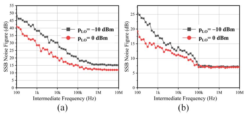
Electronics 2021, 10, 722                                                                                             6 of 12

                            maintain the fixed DC working state, degrading conversion gain of the mixer. Furthermore,
                            large current at switch-stage leads to high noise [19]. Therefore, at that case, current-
                            bleeding technology is introduced. In Figure 5b, the driver-stage current ID4 is equal to
                            switch-stage current including ID2 and ID3 plus bleeding current Ib . In other words, current
                            bleeding allows the control of the DC current for the switching transistors separately from
                            that of the driver-stage. By these means, ID4 can be higher than ID5 + ID6 and switch-stage
                            current can be lowered to reduce the flicker noise of proposed mixer.
                                 Assuming the driver-stage current ID1 in Figure 5a is equal to the driver-stage current ID4
                            in Figure 5b. Based on Equation (2), the mixer flicker noise in Figure 5a,b can be expressed as:
                                                                               4ID1 f LO
                                                            Vn,out ( f ) a =             Rl · Vn,LO ( f )                (4)
                                                                                 S LO

                                                                          4( ID1 − Ib ) f LO
                                                        Vn,out ( f )b =                      Rl · Vn,LO ( f )            (5)
                                                                                S LO
                                  Because of the bleeding current Ib , flicker noise in Equation (5) is smaller than that
                            in Equation (4). In this way, the flicker noise with current-bleeding structure in Figure 5b
                            promises smaller than that with conventional structure in Figure 5a.
                                  Referred to Figure 4, the proposed mixer adopted a resistor RC as a bleeding current
                            source. Resistances of load resistor RL and bleeding source resistor RC are selected by
                            elaborate simulation to keep good performance. In the design, RC was chosen to be 60 Ω
                            and load resistor was 800 Ω. The analysis on the mixer of static operating point shows
                            that the bleeding current Ib takes 97% of whole DC current ID4 . The drain voltages of M4 ,
                            M5 /M6 are 0.5 V and 1.1 V. The voltage drop of load resistor RL is 0.1 V, making sure the
                            headroom of this design under a 1.2 V supply voltage. However, the small resistance of RC
                            caused conversion gain loss to a certain extent. The simulation result showed that signal
                            power loss caused by RC was about 70%, leading to about 5 dB conversion gain loss.
                                  Based on the bleeding-current mixer, simulation was carried out on different LO power
                            to find a suitable one to achieve low flicker noise. Result is depicted in Figure 6, showing that
                            flicker noise is decreasing with LO power increasing. The result is in accord with Equation (3).
                            From Figure 6, the LO power is increasing from −15 dBm to 0 dBm. Larger LO power was
                            not adopted, because the 24 GHz frequency source could only offer moderate LO power in
                            a system, for example, −10 dBm. Larger LO power needs additional amplifiers and power
                            consumption, making system not cost-efficient. At last, a 0 dBm LO power was chosen.

                            Figure 6. Simulated flicker noise of mixer with different LO (local oscillator) power.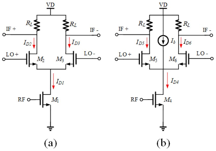
Electronics 2021, 10, 722 7 of 12
4. Results
The 90 nm SOI CMOS technology has been utilized in this work for the receiver
realization. The technology features five metal layers with two thick RF metals on the top.
The upper two RF metal layers with 3.3 um thickness have been extensively utilized for the
realization of on-chip transmission lines and spiral inductors. The design benefited from
the high resistivity of the SOI substrate; thus, the traditional patterned ground shields on
the bottom of on-chip spiral inductors could be omitted. High-Q inductors and capacitors
can be realized. In addition, all the critical on-chip interconnections are based on the
shielded co-planar transmission line structures. Taking into consideration the influence of
electromagnetic coupling between lines and passive components, elaborate and complete
EM simulation was carried out to ensure the accuracy of this design.
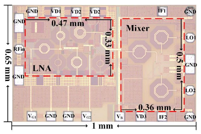
Figure 7 shows the micrograph of the realized receiver circuit. Decoupling capacitors
with 2 pF capacitance were placed between every DC pad and closest ground pad to filter
clutter from DC sources. The compact receiver chip achieves a total chip area (including the
pads) of 0.65 mm2 (1 mm × 0.65 mm). Test chips for two main building blocks namely the
LNA and mixer have also been integrated on separate dies and tested alone. Standalone
LNA and mixer occupy 0.16 mm2 and 0.18 mm2 , respectively. Chips have been bonded
on PCB for characterization. All RF signals have been provided through probe station.
Small-signal measurements were carried out with Agilent N5247A network analyzer. The
Agilent N8975A NFA offered platform for NF measurements.
Figure 7. Chip photo of the proposed receiver.
Performance of the LNA has been presented in Figure 8. The measured and simulated
small-signal S-parameters, NF, P1dB and IIP3 of LNA are depicted in Figure 8a–d, separately.
The measured S21 reached 17.2 dB of its peak at 23.8 GHz and the −3 dB bandwidth
is around 2.2 GHz from 22.8 GHz to 25 GHz. Compared with simulation results, the
deteriorated S11 and S22 worsen gain and bandwidth. The S11 is lower than −10 dB from
22.5 GHz to 26.6 GHz and S22 is under −10 dB from 23.2 GHz to 24.6 GHz. The parameter
standing for isolation from output to input S12 is below −30 dB within the whole working
band. The results in Figure 8b show that the LNA achieves an average 3 dB NF within
the 24 GHz band. The linearity performance is illustrated in Figure 8c,d. Figure 8c plots
the power gain versus input power and the IP1dB could be observed −15 dBm. The IIP3 is
found to be −5 dBm in Figure 8d.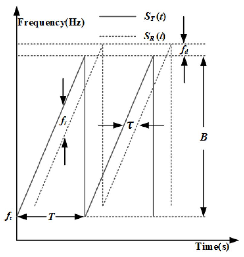
Electronics 2021, 10, 722                                                                                                         8 of 12

       Figure 8. (a) S-parameters of LNA (low-noise-amplifier); (b) NF (noise figure) of LNA; (c) P1dB of LNA; (d) IIP3 of LNA.

                                      A second set of experiments was carried out on the receiver including LNA and mixer.
                                 Another signal source has been introduced to feed the 0 dBm LO signal to mixer. The mea-
                                 surements were carried out by sweeping the RF and LO frequency with fixed IF of 125 MHz.
                                 Figure 9 presents the measured and simulated results of the receiver chip. Figure 9a shows
                                 the simulated and measured conversion gain and noise figure performance of the receiver
                                 and 20.3 dB gain and 7 dB SSB NF are achieved. Compared with the simulation results,
                                 with influence of parasitic part and test environment, the measured conversion gain is
                                 3.5 dB lower and the NF is 1 dB higher. The −3 dB bandwidth of receiver is constrained
                                 mainly by LNA, which is 2.2 GHz from 22.8 GHz to 25 GHz as well. Shown in Figure 9b is
                                 the RF and LO matching performance of the receiver. Even though measured results are
                                 worse than simulated results, the S11 is below −10 dB from 23 GHz to 27 GHz and S22 is
                                 below −10 dB from 23.2 GHz to 25.4 GHz. It means that RF port and LO port input match
                                 well, respectively. The port-to-port isolation has been characterized for proposed receiver
                                 from 21 GHz to 27 GHz and shown in Figure 9c. All the isolation levels are more than 30 dB
                                 in 24 GHz band. The LO-IF isolation is much lower, because the LO signal is fed directly to
                                 the mixer with relatively higher amplitude. With 24 GHz RF and 125 MHz IF, the input
                                 power at 1 dB gain compression point value of −22 dBm has been measured in Figure 9d.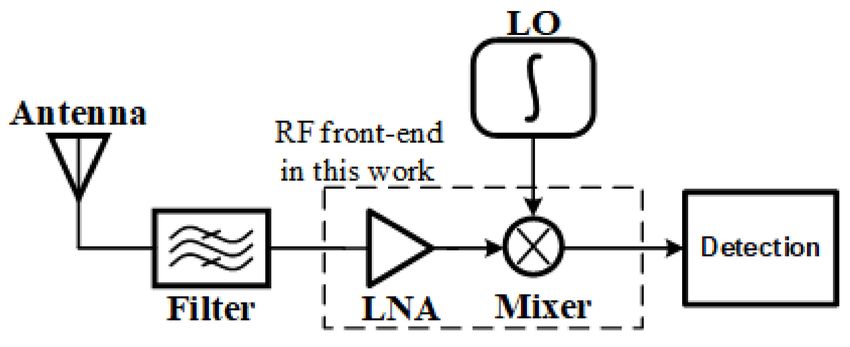
Electronics 2021, 10, 722                                                                                                   9 of 12

      Figure 9. (a) Conversion gain and NF (noise figure) of receiver; (b) S-parameters of RF (radio frequency) and LO (local
      oscillator) ports; (c) Measured port solation of receiver; (d) P1dB of receiver.

                                       Measured flicker noise results of standalone mixer and receiver are shown in Figure 10.
                                 To verify influence of LO power on flicker noise, two LO power are set to −10 dBm and
                                 0 dBm. The IF is selected from 100 Hz to 10 MHz and log scale is used to make results
                                 clear and intuitive. The results indicate that larger LO power can reduce the flicker noise
                                 of receiver, same as the simulated results. From Figure 10a, the flicker noise of mixer is
                                 higher than above simulation result. The reason may be inexact noise model of transistor
                                 and loss introduced by measure equipment. The literature often uses the term “knee-point”
                                 for the frequency below which the flicker noise dominates over thermal noise. Commonly,
                                 we consider the frequency at which the noise figure is 3 dB higher than the lowest noise
                                 figure to be knee-point. With a 0 dBm LO power, the knee-point is observed to be 60 kHz.
                                 Compared with the 48 kHz ideal simulated knee-point reported in [18], this circuit achieved
                                 a relatively low noise corner. In Figure 10b, because of the former-stage high-gain LNA,
                                 the contribution about NF of mixer part has been reduced. Then, a relatively low noise is
                                 achieved. Furthermore, as shown in Figure 10, noise under two different LO power stays
                                 almost the same when IF is larger than 100 kHz. With parameters in Equation (1), 100 kHz
                                 IF results from 30 m target distance. In a real scenario, when the target distance is larger
                                 than 30 m, a lower LO power can be used to save power consumption whilst introducing
                                 no more noise.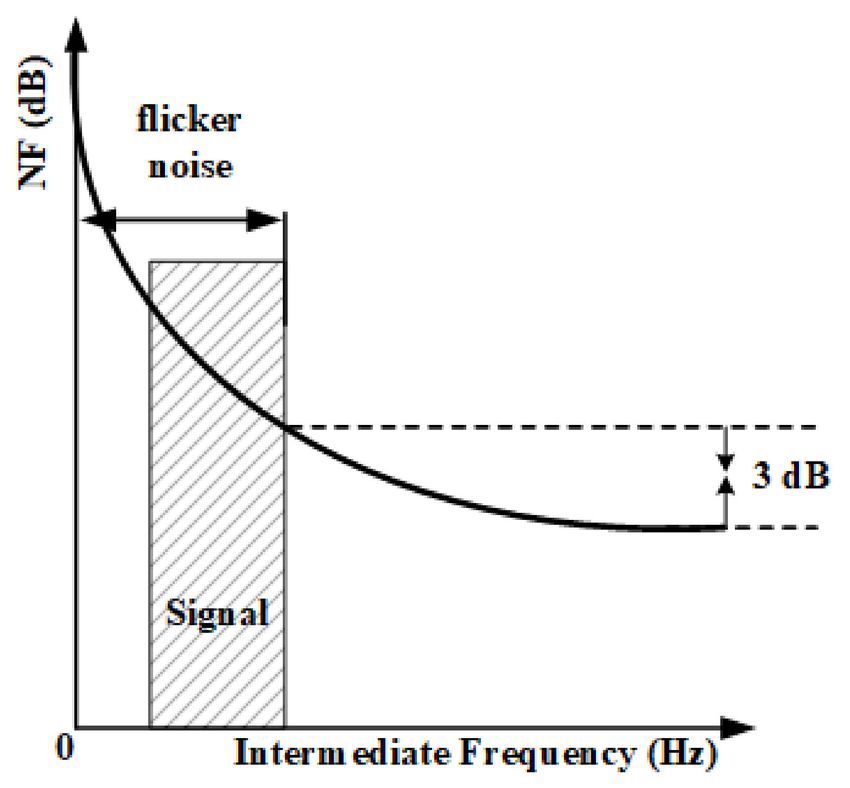
Electronics 2021, 10, 722                                                                                                       10 of 12

                            Figure 10. (a) Flicker noise results of mixer; (b) flicker noise results of receiver.

                                       Table 2 compares the realized receiver performance with the published state-of-art
                                  K-band receivers. From this comparison, it can be seen that the realized 24 GHz CMOS
                                  receiver compares the state-of-the-art realizations with a balanced performance even in
                                  a non-superior process. The gain is not so high as [20] because high-gain variable-gain
                                  amplifier (VGA) can be integrated in later design easily. This design achieves a knee-point
                                  of 60 kHz. It’s the first time to report a low flicker noise measured result. In order to
                                  distinguish the power consumption of bias circuit is included or not, the PDC part has been
                                  divided into two lines: PDC1 and PDC2 . The former stands for the power consumption
                                  including the bias circuit and the latter stands for the power consumption excluding the
                                  bias circuit. As talked above, the linearity restriction can be loosened in FMCW application,
                                  so the −22 dBm IP1dB is adequate.

                                                Table 2. Performance comparison table.

                             This Work                       [20]                       [21]               [22]        [23] 1
    Technology               90 nm SOI             0.13 um CMOS                    65 nm CMOS         65 nm CMOS     45 nm SOI
      Inclusion             LNA + Mixer          LNA + Mixer + VGA                 LNA + Mixer        LNA + Mixer   LNA + Mixer
   RF/IF (GHz)                24/0.125                  24/0.1                       24/0.002            21.5/0.1     24/NA
       CG (dB)                  20.3                      36                           28.3                14.5         26.2
       NF (dB)                    7                       9.9                           5                   5.7          5.6
    IP1dB (dBm)                 −22                      −35                           −28                 −40          NA
  Knee-point (kHz)               60                      NA                            NA                  NA           NA
     PDC1 (mW)                 21.1 1                    40.8                           26                 NA           NA
     PDC2 (mW)                   16                      NA                            NA                 0.683         NA
   Area 2 (mm2 )                0.65                      0.8                          0.66                 0.4         NA
                                                   1   simulation results; 2 including pads.

                                  5. Conclusions
                                       In this paper, a low-noise 24 GHz direct conversion receiver for FMCW ranging radar
                                  is designed and fabricated in 90 nm SOI CMOS technology. A low-noise and low-power
                                  LNA is proposed. To enhance gain of the receiver and reduce NF, the SNIM method
                                  was used in the input. Neutralized technology and boost inductors were introduced to
                                  improve performance. A 24 GHz current-bleeding mixer was introduced and the factors
                                  influencing flicker noise have been discussed. The measured results show the proposed
                                  receiver exhibits 20.3 dB peak gain and 7 dB SSB NF. A −22 dBm IP1dB and well-matched
                                  RF port S11 and LO port S22 have been measured. More than 30 dB isolations between RF,
                                  LO and IF ports are obtained within working frequency band. Flicker noise of both mixer
Electronics 2021, 10, 722 11 of 12
and receiver are measured and the knee point of receiver is observed 60 kHz. Combined
with the FMCW principle, the receiver indicates when the target distance is larger than
30 m, a lower LO power can be used to save power consumption. The receiver consumes
only 16 mW with chip area of 0.65 mm2 including pads. It suggests that the proposed SOI
CMOS DCR receiver can be a promising candidate for FMCW ranging radar.
Author Contributions: Conceptualization, D.L.; methodology, Q.X.; software, J.H.; validation, J.L.;
resources, H.C.; writing—review and editing, B.S.; project administration, H.L. All authors have read
and agreed to the published version of the manuscript.
Funding: This work was supported by the National Key Research and Development Program of
China under Grant No. 2016YFA0202304 and 2016YFA0201903, General Program of National Natural
Science Foundation of China under Grant No.61674168 and 61504165, as well as the Opening Project of
Key Laboratory of Microelectronics Devices and Integrated Technology, Institute of Microelectronics,
Chinese Academy of Sciences.
Acknowledgments: The authors would like to thank Yankui Li for the measurement support.
Conflicts of Interest: The authors declare no conflict of interest. The funders had no role in the design
of the study; in the collection, analyses, or interpretation of data; in the writing of the manuscript, or
in the decision to publish the results.
References
1. Mazzanti, A.; Sosio, M.; Repossi, M.; Svelto, F. A 24 GHz Subharmonic Direct Conversion Receiver in 65 nm CMOS. IEEE Trans.
Circuits Syst. I Regul. Pap. 2010, 58, 88–97. [CrossRef]
2. Ragonese, E.; Scuderi, A.; Giammello, V.; Messina, E.; Palmisano, G. A fully integrated 24GHz UWB radar sensor for automotive
applications. In Proceedings of the 2009 IEEE International Solid-State Circuits Conference—Digest of Technical Papers, San
Francisco, CA, USA, 8–12 February 2009; pp. 306–307. [CrossRef]
3. Subramanian, V.; Zhang, T.; Boeck, G. Low Noise 24 GHz CMOS Receiver for FMCW Based Wireless Local Positioning. IEEE
Microw. Wirel. Compon. Lett. 2011, 21, 553–555. [CrossRef]
4. Evans, R.J.; Farrell, P.M.; Felic, G.; Duong, H.T.; Le, H.V.; Li, J.; Li, M.; Moran, W.; Morelande, M.R.; Skafidas, E. Consumer radar:
Technology and limitations. In Proceedings of the International Conference on Radar, Adelaide, Australia, 9–12 September 2013;
pp. 21–26. [CrossRef]
5. Park, J.; Ryu, H.; Ha, K.-W.; Kim, J.-G.; Baek, D. 76–81-GHz CMOS Transmitter With a Phase-Locked-Loop-Based Multichirp
Modulator for Automotive Radar. IEEE Trans. Microw. Theory Tech. 2015, 63, 1399–1408. [CrossRef]
6. Luo, T.-N.; Wu, C.-H.E.; Chen, Y.-J.E. A 77-GHz CMOS Automotive Radar Transceiver With Anti-Interference Function. IEEE
Trans. Circuits Syst. I Regul. Pap. 2013, 60, 3247–3255. [CrossRef]
7. Ginsburg, B.P.; Subburaj, K.; Samala, S.; Ramasubramanian, K.; Singh, J.; Bhatara, S.; Murali, S.; Breen, D.; Moallem, M.; Dandu,
K.; et al. A multimode 76-to-81GHz automotive radar transceiver with autonomous monitoring. In Proceedings of the 2018 IEEE
International Solid-State Circuits Conference—(ISSCC), San Francisco, CA, USA, 11–15 February 2018; pp. 158–160. [CrossRef]
8. Dudek, M.; Nasr, I.; Bozsik, G.; Hamouda, M.; Kissinger, D.; Fischer, G. System Analysis of a Phased-Array Radar Applying
Adaptive Beam-Control for Future Automotive Safety Applications. IEEE Trans. Veh. Technol. 2015, 64, 34–47. [CrossRef]
9. Wei, P.; Diao, S.; Huang, D.; Fu, Z.; Lin, F. A K-Band Down-Conversion mixer design with integrated baluns in 65nm CMOS. In
Proceedings of the Proceedings of 2012 5th Global Symposium on Millimeter-Waves, Harbin, China, 27–30 May 2012; pp. 282–285.
[CrossRef]
10. Ali, M.K.; Hamidian, A.; Malignaggi, A.; Arnous, M.T.; Boeck, G. Low flicker noise high linearity direct conversion mixer for
K-band applications in a 90 nm CMOS technology. In Proceedings of the 2014 20th International Conference on Microwaves,
Radar and Wireless Communications (MIKON), Gdańsk, Poland, 16–18 June 2014; pp. 1–4. [CrossRef]
11. Ahn, D.; Kim, D.-W.; Hong, S. A K-Band High-Gain Down-Conversion Mixer in 0.18 µm CMOS Technology. IEEE Microw. Wirel.
Compon. Lett. 2009, 19, 227–229. [CrossRef]
12. Krishnaswamy, H.; Hashemi, H. A Fully Integrated 24GHz 4-Channel Phased-Array Transceiver in 0.13 µm CMOS Based on a
Variable-Phase Ring Oscillator and PLL Architecture. In Proceedings of the IEEE International Solid-State Circuits Conference.
Digest of Technical Papers, San Francisco, CA, USA, 11–15 February 2007; pp. 124–591. [CrossRef]
13. Li, D.; Xia, Q.; Huang, J.; Li, J.; Chang, H.; Sun, B.; Liu, H. A 4-mW Temperature-STable 28 GHz LNA with Resistive Bias Circuit
for 5G Applications. Electronics 2020, 9, 1225. [CrossRef]
14. Ma, T.; Deng, W.; Chen, Z.; Wu, J.; Zheng, W.; Wang, S.; Qi, N.; Liu, Y.; Chi, B. A CMOS 76–81-GHz 2-TX 3-RX FMCW Radar
Transceiver Based on Mixed-Mode PLL Chirp Generator. IEEE J. Solid-State Circuits 2019, 55, 233–248. [CrossRef]
15. Huang, B.-J.; Lin, K.-Y.; Wang, H. Millimeter-Wave Low Power and Miniature CMOS Multicascode Low-Noise Amplifiers with
Noise Reduction Topology. IEEE Trans. Microw. Theory Tech. 2009, 57, 3049–3059. [CrossRef]Electronics 2021, 10, 722 12 of 12
16. Nguyen, T.-K.; Kim, C.-H.; Ihm, G.-J.; Yang, M.-S.; Lee, S.-G. CMOS Low-Noise Amplifier Design Optimization Techniques. IEEE
Trans. Microw. Theory Tech. 2004, 52, 1433–1442. [CrossRef]
17. Yu, Z.; Feng, J.; Guo, Y.; Li, Z. Analysis and design of a V-band low-noise amplifier in 90 nm CMOS for 60 GHz applications.
IEICE Electron. Express 2015, 12. [CrossRef]
18. Kong, Y.; Yan, N. High gain and low flicker noise down-conversion mixer applied in 24GHz FMCW radar. In Proceedings of the
2018 IEEE MTT-S International Wireless Symposium (IWS), Chengdu, China, 6–10 May 2018; pp. 1–4. [CrossRef]
19. Lai, D.; Chen, Y.; Wang, X.; Chen, X. A CMOS Single-Differential LNA and current bleeding CMOS mixer for GPS Re-
ceivers. In Proceedings of the 2018 2010 IEEE 12th International Conference on Communication Technology, Nanjing, China,
11–14 November 2010; pp. 677–680. [CrossRef]
20. Wang, H.; Jiao, C.; Zhang, L.; Zeng, D.; Yang, D.; Wang, Y.; Yu, Z. A low-power ESD-protected 24GHz receiver front-end with
π-type input matching network. In Proceedings of the 2011 IEEE International Symposium of Circuits and Systems (ISCAS), Rio
de Janeiro, Brazil, 15–18 May 2011; pp. 2877–2880. [CrossRef]
21. Cheng, J.; Hsieh, C.; Wu, M.; Tsai, J.; Huang, T. A 0.33 V 683 uw K-Band Transformer-Based Receiver Front-End in 65 nm CMOS
Technology. IEEE Microw. Wirel. Compon. Lett. 2015, 25, 184–186. [CrossRef]
22. Ding, Y.; Vehring, S.; Maurath, D.; Gerfers, F.; Boeck, G. A 24 GHz Zero-IF IQ-receiver using low-noise quadrature sig-
nal generation. In Proceedings of the 2017 IEEE Asia Pacific Microwave Conference (APMC), Kuala Lumpur, Malaysia,
13–16 November 2017; pp. 1226–1229. [CrossRef]
23. Wang, Y.; Cui, J.; Zhang, R.; Sheng, W. Fully differential Ultra-wideband LNA-Mixer for K to Ka Band receiver in 45nm CMOS
SOI technology. In Proceedings of the 2019 IEEE Asia-Pacific Microwave Conference (APMC), Singapore, 10–13 December 2019;
pp. 16–18. [CrossRef]You can also read