Lithiation-Induced Shuffling of Atomic Stacks
←
→
Page content transcription
If your browser does not render page correctly, please read the page content below
Letter

                                                                                                                                pubs.acs.org/NanoLett

Lithiation-Induced Shuffling of Atomic Stacks
Anmin Nie,†,#,§ Yingchun Cheng,‡,§ Yihan Zhu,∥,§ Hasti Asayesh-Ardakani,† Runzhe Tao,#
Farzad Mashayek,¶ Yu Han,∥ Udo Schwingenschlögl,‡ Robert F. Klie,# Sreeram Vaddiraju,⊥
and Reza Shahbazian-Yassar*,†,#,¶
†
 Department of Mechanical Engineering-Engineering Mechanics, Michigan Technological University, 1400 Townsend Drive,
 Houghton, Michigan 49931, United States
‡
 Department of Physical Science and Engineering, King Abdullah University of Science & Technology, Thuwal, 23955-6900,
 Kingdom of Saudi Arabia
∥
  Advanced Membranes and Porous Materials Center, Physical Sciences and Engineering Division, King Abdullah University of
 Science & Technology, Thuwal, 23955-6900, Kingdom of Saudi Arabia
⊥
  Artie McFerrin Department of Chemical Engineering, Texas A&M University, 3122 TAMU, College Station, Texas 77843, United
 States
#
 Department of Physics, University of Illinois at Chicago, Chicago, Illinois 60607, United States
¶
  Mechanical and Industrial Engineering Department, University of Illinois at Chicago, Chicago, Illinois 60607, United States
    *
    S Supporting Information

    ABSTRACT: In rechargeable lithium-ion batteries, under-
    standing the atomic-scale mechanism of Li-induced structural
    evolution occurring at the host electrode materials provides
    essential knowledge for design of new high performance
    electrodes. Here, we report a new crystalline−crystalline phase
    transition mechanism in single-crystal Zn−Sb intermetallic
    nanowires upon lithiation. Using in situ transmission electron
    microscopy, we observed that stacks of atomic planes in an
    intermediate hexagonal (h-)LiZnSb phase are “shuffled” to
    accommodate the geometrical confinement stress arising from
    lamellar nanodomains intercalated by lithium ions. Such
    atomic rearrangement arises from the anisotropic lithium diffusion and is accompanied by appearance of partial dislocations.
    This transient structure mediates further phase transition from h-LiZnSb to cubic (c-)Li2ZnSb, which is associated with a nearly
    “zero-strain” coherent interface viewed along the [001]h/[111]c directions. This study provides new mechanistic insights into
    complex electrochemically driven crystalline−crystalline phase transitions in lithium-ion battery electrodes and represents a noble
    example of atomic-level structural and interfacial rearrangements.
    KEYWORDS: lithium-ion batteries, in situ STEM, atomic scale, phase transition, Zn4Sb3 nanowires

N      umerous research efforts have been devoted toward the
       next generation of lithium ion batteries (LIBs) due to the
ever-growing need for high specific energy density and good
                                                                              Intermetallic alloys often undergo electrochemically driven
                                                                           crystalline−crystalline phase transitions that results in complex
                                                                           charge−discharge cycling performance. In particular, Sb-based
cycling performance.1−3 The main challenge facing LIBs is the              intermetallic alloys have received imminence attention in
discovery of new electrode materials with promising electro-               rechargeable battery community for their high theoretical
                                                                           capacities and suitable operating voltages.14−16 New and
chemical lithium ion storage properties and a mechanistic
                                                                           elegant concepts are introduced behind the design of these
understanding of the reactions taking place in the cells.4,5 For
                                                                           Sb-based intermetallic electrodes due to the strong structural
next generation LIBs, electrochemically driven phase transitions           relationship with their lithiated products. For instance, SnSb
are widely involved in the electrode materials and also closely            electrodes provide a high capacity and controllable volume
linked with LIBs performance.6−8 Recent in situ transmission               expansion due to both Sn and Sb metals reacting with Li and
electron microscopy (TEM) works have documented Li-                        distributing a ductile Sn phase during cycling.17,18 A reversible
induced crystalline to amorphous phase transitions9,10 or Li-              process of lithium insertion and metal extrusion was suggested
induced atomic ordering within amorphous matrix.11,12
However, direct atomic-scale observations of electrochemically             Received: June 22, 2014
driven crystalline−crystalline phase transition in LIBs have               Revised: August 14, 2014
hardly been achieved.13                                                    Published: August 26, 2014

                              © 2014 American Chemical Society      5301                        dx.doi.org/10.1021/nl502347z | Nano Lett. 2014, 14, 5301−5307
Nano Letters                                                                                                                                            Letter

Figure 1. Morphology and microstructural evolution of individual Zn4Sb3 nanowires during charging against lithium metal. (a) Time-lapse
morphology evolution of the Zn4Sb3 nanowire. As the reaction front (marked by red arrow) passed by, the nanowire expanded both in radial and
axial direction. Cracks and some nanoparticles formed at the late stage of lithiation. (b) SAED pattern taken from area S1 (marked in (a)) with [11̅0]
zone axis before reaction front passing by. (c) SAED pattern taken from area S2 (marked in (a)) after the lithiation. (d) Intensity profile from the
electron diffraction pattern shown in (c) along the red arrow line. The peaks corresponding with the specific rings in the electron diffraction pattern
are indexed to be LiZnSb, Zn, LiZn, and either Li2ZnSb or Li3Sb.

in Cu2Sb electrodes with a stable face-centered-cubic (fcc) Sb                 Sb alloys. Taking advantage of an aberration-corrected scanning
host framework for both the incoming and extruded metal                        transmission electron microscope (STEM) with potential to
atoms.19 In addition, quasi-intercalation concept was proposed                 identify atomic distances as small as 0.7 Å20 and image the light
in orthorhombic ZnSb due to the layered structures of ZnSb                     elements such as oxygen,21 lithium,22,23 and hydrogen24 in
and hexagonal LiZnSb (h-LiZnSb).14 Most of these mecha-                        crystal structures by embracing the annular bright field (ABF)
nisms were proposed in light of ex situ X-ray diffraction (XRD),                STEM technique, we directly observed the dynamics of
which has intrinsic limitations in resolving aperiodic compo-                  lithiation in individual single-crystal Zn4Sb3 nanowires. The
nents like strains, defects, and disorders at high spatial                     kinetics of lithiation was found to be highly anisotropic and
resolution. Therefore, the dynamic nature of these interesting                 relevant to the interfacial structures of the reaction front at
phenomena does need to be further explored by in situ tools.                   different stages of lithiation. Atom-resolved images of interfacial
  In this work, we reveal a new type of lithiation-triggered                   structures captured at different lithiation stages clearly reveal
crystalline−crystalline phase transitions at atomic-scale for Zn−              that the initial lithiation of Zn4Sb3 nanowire proceeded via
                                                                        5302                          dx.doi.org/10.1021/nl502347z | Nano Lett. 2014, 14, 5301−5307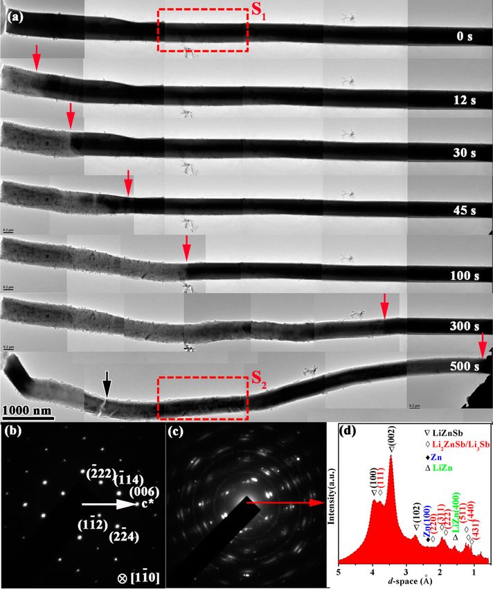
Nano Letters                                                                                                                                         Letter

Figure 2. Atomic resolution STEM images of phase transition from h-LiZnSb to c-Li2ZnSb. (a) Atomic resolution HAADF image for h-LiZnSb
along [001]h zone axis. Inset is the corresponding colored HAADF image. (b) ABF image for h-LiZnSb along [001]h zone axis. Top inset is the
corresponding colored ABF image. The colored ABF image highlights the Li visibility as green. Bottom inset corresponds to intensity profiles along
P1 and P2 from HAADF and ABF images, respectively. The presence of Li atoms is clearly detectable in the intensity profile along P2. (c) Atomic
resolution HAADF image of the interfacial structure between h-LiZnSb (Above red dotted line and along [001]h zone axis) and c-Li2ZnSb (Below
red dotted line and along [111]c zone axis). The two areas show different stacking sequences (Top: ABABAB, Bottom: ABCABC). (d) Atomic
resolution HAADF image shows c-Li2ZnSb [111]c projection after the interface migration.

formation of intermediate h-LiZnSb and cubic Li2ZnSb (c-                     is given by selected area electron diffraction (SAED) patterns
Li2ZnSb) phases before transforming to Li3Sb with Zn                         (Figure 1b and c). Figure 1b shows the SAED pattern taken
extrusion. Interestingly, we found that the phase transition                 along the [11̅0] zone axis from the section of the nanowire
from h-LiZnSb to c-Li2ZnSb is triggered by stress-induced                    marked as S1. From the SAED pattern, it can be conclude that
shuffling of stacked atomic layers due to the anisotropic                      the nanowire was monocrystalline with a [001] growth
transport of lithium ions.                                                   direction before lithiation, which is consistent with the
   The general chemical and microstructural features of pristine             atomic-resolution STEM images (Supporting Information
Zn4Sb3 nanowire are presented in Figure S1 and S2                            Figure S2). After lithiation, the SAED pattern (Figure 1c)
(Supporting Information). The Zn4Sb3 nanowires are con-                      taken from the same area of the nanowire marked as S2 shows
firmed to be monocrystalline with the [001] growth direction.                 diffraction rings, which indicates the formation of nanocrystals
The Zn4Sb3 nanowire was subjected to lithiation process by                   of new phases. The corresponding intensity profile (Figure 1d)
using an in situ electrochemical cell9 inside TEM (Supporting                along the red arrow line in Figure 1c shows peaks at different
Information Figure S3). Figure 1a (Supporting Information                    position (d-spacing), evidencing the formation of Zn, h-LiZnSb,
Movie S1) shows the propagation of the reaction front in a                   c-Li2ZnSb, Li3Sb, and LiZn. Due to close d-spacing, it is
Zn4Sb3 nanowire during lithiation. As the reaction front                     challenging to explicitly distinguish between c-Li2ZnSb (S.G.
(marked by the red arrow) propagated along the longitudinal                  F4̅3m, a = 6.47 Å, JCPDS Card No.71-0222) and Li3Sb (S.G.
direction, the TEM image contrast changed from dark to gray                  Fm3m, a = 6.57 Å, JCPDS Card No. 04-0791) phases from the
due to phase transition. After lithiation, this nanowire elongated           intensity profile of the SAED pattern (Supporting Information
by about 10%, the diameter increased by about 15%, and the                   Figure S4), which is straightforward, however, for high-
total volume expanded by about 45%. In addition, nanocracks                  resolution imaging.
were formed in the lithiated section of the nanowire matrix as                  Followed by the electrochemically driven solid-state
pointed out by the black arrow in Figure 1a. More detailed                   amorphization of Zn4Sb3, nucleation and growth of h-LiZnSb
structure and phase characterization before and after lithiation             nanocrystals were observed in the lithiated amorphous
                                                                      5303                         dx.doi.org/10.1021/nl502347z | Nano Lett. 2014, 14, 5301−5307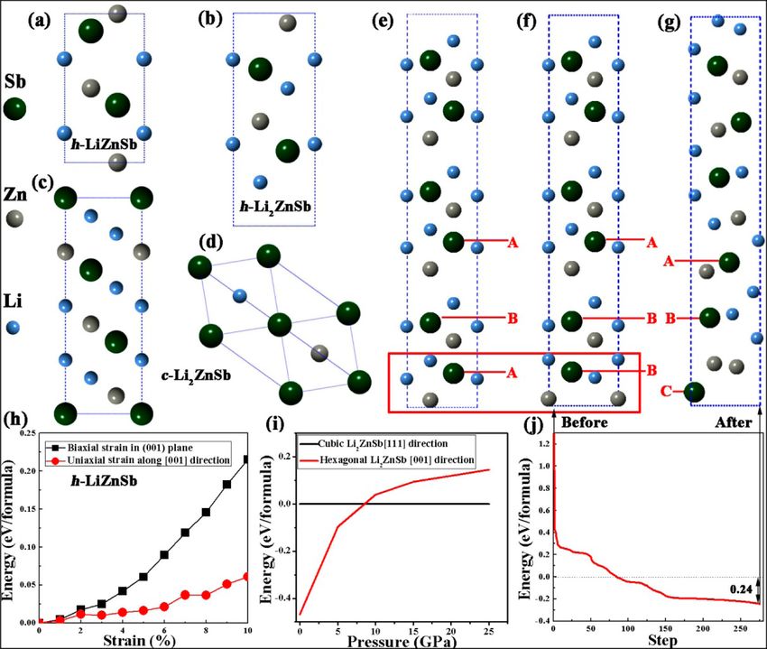
Nano Letters Letter
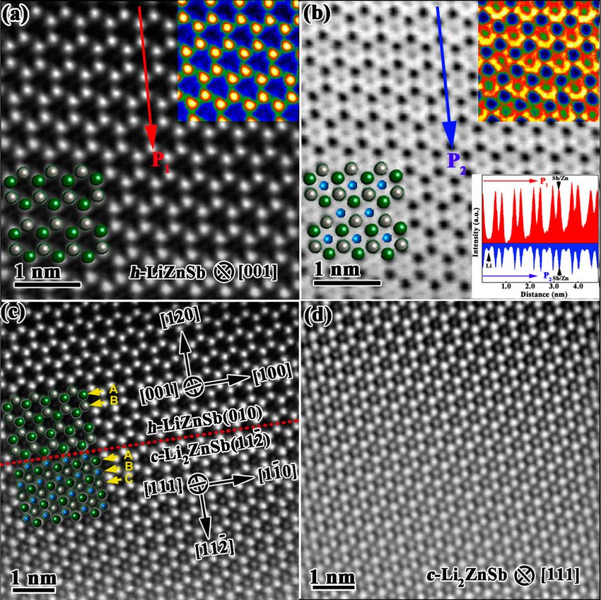
Figure 3. Direct imaging of phase transition from h-LiZnSb to c-Li2ZnSb. (a) Atomic resolution HAADF image showing h-LiZnSb structure viewed
from [100]h direction. The Sb atom layers show ABABAB stacking sequence along [001]h direction. (b) Atomic resolution HAADF image showing
intermediate structure from h-LiZnSb to c-Li2ZnSb. The domains with the ABC stacking sequence, which are named I, II, and III are highlighted by
blue color. (c) Atomic resolution HAADF image of perfect c-Li2ZnSb structure along [11̅0]c direction. The Sb layers show ABCABC stacking
sequence along [111]c direction. (d) Strain mapping along [001]h direction of the h-LiZnSb structure calculated by using GPA from HAADF image
(a). (e) Strain mapping normal to the stacking Sb layers of the intermediate structure calculated by using GPA from HAADF image (b). (f) Strain
mapping along [111]c direction of the c-Li2ZnSb structure calculated by using GPA from HAADF image (c). The color scale is from −10% to 10%.
(g) Schematic representation of phase transition from h-LiZnSb to c-Li2ZnSb. Yellow atoms indicate the new coming lithium ion and black arrows
show the stress direction. Here, the formulas of LiZnSb and Li2ZnSb indicate nonintercalated and intercalated domains, respectively.
LixZn4Sb3 matrix (Supporting Information Figure S5 and S6). LiZnSb structure can be derived by filling one-half of the
Figure 2 shows atomic resolution high angle annular dark field tetrahedral voids periodically with the Zn-cations and all the
(HAADF) and corresponding ABF images of a crystalline octahedral voids with Li ions in an hexagonal close-packed
particle inside the lithiated nanowire, which later was identified (hcp-type) Sb sublattice (Supporting Information Figure S7).
as h-LiZnSb (S.G. P63mc, JCPDS Card No. 34-0508) structure The h-LiZnSb phase is made of Zn/Sb/Li atomic layers stacked
viewed along the [001]h direction. Due to the Z1.7 dependence periodically along the [001]h direction, where Zn/Sb atoms
of HAADF contrast,25 the light elemental atoms (such as Li and alternatively occupy the A/B sites while Li atoms occupy the C
O) can hardly gain intensity in the HAADF image. Thus, in the sites. Here, A, B, and C refer to distinct atomic layers
HAADF image (Figure 2a), bright spots correspond to the perpendicular to the stacking direction.
overlapped Sb (Zn) atomic columns with the corresponding After further lithiation, the phase transition from h-LiZnSb to
intensity line profile along direction P1 as shown in the inset of c-Li2ZnSb was observed. The c-Li2ZnSb phase consists of a
Figure 2b. A false-colored HAADF image with more more densely packed lattice where Zn and Li atoms occupy all
comprehensible contrast was inserted into Figure 2a. The Sb the octahedral and tetrahedral voids formed by the fcc-type Sb
and Zn atomic-columns cannot be discriminated due to the sublattice. Hence, the Sb/Zn/Li/Li atomic layers produced a
overlap of them along the [001] zone axis. This well stacking sequence of ABC along the [111]c direction after full
arrangement is also revealed by the intensity line profile Li intercalation (Supporting Information Figure S8). Figure 2c
along direction P2 in the inset of the ABF image in Figure 2b. shows an atomic resolution HAADF image recorded at a
In comparison with profile P1 in HAADF image, the Li atom lithiated region with the two phases intergrown inside one
columns can be directly observed in profile P2. Actually, the h- nanoparticle. The image above the red dotted line shows
5304 dx.doi.org/10.1021/nl502347z | Nano Lett. 2014, 14, 5301−5307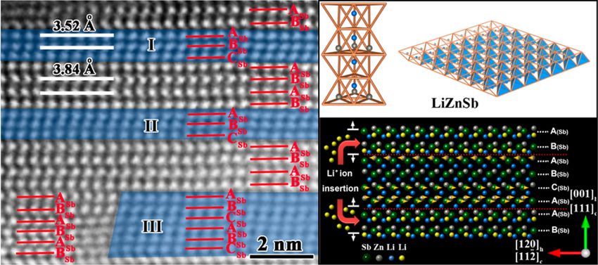
Nano Letters                                                                                                                                             Letter

Figure 4. Ab initio simulations of phase transition from h-LiZnSb to c-Li2ZnSb. (a) Atomic structure of primitive cell of h-LiZnSb viewed along
[100]h. (b) Atomic structure of primitive cell of h-Li2ZnSb viewed along [100]h. (c) Supercell of c-Li2ZnSb viewed along [11̅0]c. (d) Atomic
structure of primitive cell of c-Li2ZnSb viewed along [111]c. (e) 1 × 1 × 3 supercell of h-Li2ZnSb. (f) Supercell of h-Li2ZnSb by sliding one LiLiZnSb
layer along [11̅0]h direction before relaxation. The bottom Sb layer was moved from A site to B site. (g) Supercell of h-Li2ZnSb by sliding one
LiLiZnSb layer after relaxation. The bottom Sb layer trends to occupy C site after relaxation. (h) Energy-strain curve of h-LiZnSb under biaxial strain
in (001)h plane and uniaxial strain along [001]h direction. (i) Energy evolution by applying pressure along h-Li2ZnSb [001] direction and c-Li2ZnSb
[111]c direction. (j) Energy evolution of relaxation of structure in (f).

hexagonally arranged bright atomic columns, which is                            region. The whole domain is occupied by c-Li2ZnSb structure
characteristic for the AB stacked h-LiZnSb phase projected                      projected with [111]c direction with ABC stacking sequence.
along the [001]h direction. The image below the red dotted line                    Figure 3 provides a different view of the lithiation induced
shows the existence of additional atomic columns at the center                  reordering of the stacked atoms between h-LiZnSb and c-
of hexagonal shaped atomic columns. Since Li ions are                           Li2ZnSb from their respective [100]h and [110̅ ]c zone axes.
completely invisible by a HAADF detector due to their low                       From this projection, the crystallographic positions (i.e., ABC
scattering ability, the atomic columns observed at the centers of               sites) of different atomic layers belonging to either hexagonal or
the hexagons corresponds to Sb or Zn atomic column occupied                     cubic phases can be straightforwardly viewed based on their
at the C sites and are indicative of the formation of the c-                    relative displacement along the [120]h/[112̅]c directions. Figure
Li2ZnSb or Li3Sb domains projected along the [111]c direction.                  3a shows an atomic HAADF image of the h-LiZnSb structure
The cubic domain structure is further determined to be c-                       viewed along the [100]h direction. In Figure 3a, the brighter
Li2ZnSb by the energy dispersive X-ray spectroscopy (EDS)                       atomic columns can be clearly identified as Sb sites from the Z-
analysis due to the presence of Zn atoms and HAADF images                       contrast HAADF image and the Sb sublattice exhibits the
viewing along another zone axis (Supporting Information                         ASbBSb stacking mode. Upon further lithiation, we observed
Figure S9). In Figure 2c, notably, Sb/Zn atomic columns at the                  new structural domains (marked as I, II, and III) that are
C sites are less bright near the domain boundary compared                       sandwiched by neighboring ASbBSb-stacked atomic layers and
with those equivalent sites in the c-Li2ZnSb domain below,                      deviate from the pristine h-LiZnSb structure (Figure 3b). These
which can be possibly explained by the presence of the inclined                 domains correspond to several ASbBSbCSb-stacked atomic layers,
diffusional interface that is not parallel to the (010)h plane.                  which appear in the typical cubic fcc phase. Partial dislocation
Perfect coherent relationship between the two phases indicates                  cores (b = 1/3 ⟨120⟩), which were observed in the middle
nearly zero interfacial strain and is essential for a high interface            between Domain III and its left part, indicate transient
mobility during lithium intercalation associated with the phase                 displacement of the atomic layer between the AB and ABC
transition kinetics.26,27 Figure 2d shows an atomic resolution                  stacking domains due to partial lithiation. The lithiation
HAADF image recorded after the interface swept across the                       continues until all the ASbBSb stacks belonging to h-LiZnSb
                                                                         5305                          dx.doi.org/10.1021/nl502347z | Nano Lett. 2014, 14, 5301−5307
Nano Letters Letter
phase are transformed to new ASbBSbCsb stacking mode in c- and 4e. Figure 4h shows the energy-strain curve of h-LiZnSb
Li2ZnSb phase (Figure 3c). Figure 3d−f show the strain under biaxial strain in the (001)h plane and uniaxial strain along
mappings along the stacking direction ([001]h or [111]c) the [001]h direction. The energy required for uniaxial strain
derived by geometric phase analysis (GPA)28 from the HAADF along the [001]h direction is much smaller than that for biaxial
images of Figure 3a−c. In the pristine h-LiZnSb and fully strain in the (001)h plane, which suggests Li ion is easier to
lithiated c-Li2ZnSb (Figure 3d and f), there is no obvious strain intercalate and diffuse between the (001)h planes, which
fluctuation. At the initial lithiation stage of h-LiZnSb (Figure coincides well with our experimental observations. This is also
3e), it is surprising to note that those AB-stacked domains similar to Li intercalation in layered materials, such as
undergo large tensile strain (as measured d spacing ∼ 3.84 Å) graphite.30 In addition, the energy-strain curve also suggests
while the newly formed ABC-stacked ones experience great that the lattice expands more along the [001]h direction than in
compressive strain (d spacing ∼ 3.52 Å, i.e., I, II, and III the (001)h plane, which provides a simple explanation why
domains in Figure 3b), assuming that the upper left region is coexistence of the h-LiZnSb and c-Li2ZnSb phases results in
unlithiated and has a zero strain. Despite the fact that perfect c- perfect coherency viewed along the [001]h direction (Figure
Li2ZnSb phase should have a larger hkl interlayer spacing (3.74 2c) and strain fluctuations viewed along the [100]h direction
Å) than that (3.57 Å) of the h-LiZnSb phase, we here attribute (Figure 3b, e).
the increased interlayer separation of h-LiZnSb domains to the Figure 4a−j provides a more in-depth understanding on why
effect of partial Li intercalation at initial lithiation stage. The h-Li2ZnSb structure does not form as a stable phase during
lithiation occurs at different layers and forms highly tensile lithiation. Figure 4b shows a hypothetical situation where Li
domains due to the facilitated intercalation and diffusion of the intercalation results in h-Li2ZnSb formation. This consideration
lithium ions along the (001)h planes.29 Those nonintercalated is in conflict with our observation that Li2ZnSb is in the cubic
domains sandwiched between neighboring partially lithiated phase. According to our HAADF imaging (Figure 2 and Figure
domains would thus experience great compressive stresses, 3), the correspondent lattice parameters of h-LiZnSb and c-
which account for the rearrangements of the atomic layers and Li2ZnSb are close. We constrain the lattice parameters of
alternation of their stacking order as observed in the domains I, hexagonal and cubic Li2ZnSb as that of pristine h-LiZnSb with
II, and III. Further lithiation in the rearranged domains with applying pressure along the [001]h and [111]c directions. The
shuffled atomic stacks (i.e., domains I, II, and III) eventually total energy of h-Li2ZnSb is 0.17 eV/formula larger than that of
drive all the atomic layers to the ABC stacked Li2ZnSb cubic c-Li2ZnSb by calculation (Figure 4i). Therefore, the h-Li2ZnSb
phase, and is accompanied by the bulk stress relief through is a metastable phase during Li intercalation under constrain
volume expansion. Based on these experimental observations, a and should transform to cubic phase to lower the total energy.
hypothetical mechanism of the lithiation induced crystalline− The transition from h-Li2ZnSb to c-Li2ZnSb can be explained
crystalline phase transition is proposed here in Figure 3g. by the sliding mechanism as shown in Figure 4e-f. The h-
Owing to the highly anisotropic lithiation kinetics in h-LiZnSb Li2ZnSb contains two layers of Li in the (001)h plane. Due to
that has more closely packed Sb atomic layers on the (001) weak interaction between Li layers and the Zn/Sb layer, it is
plane, the in-plane lithium diffusion is expected to be much expected that the sliding of different layers in the (001)h plane
faster than the out-of-plane lithium hopping between different is energy favorable. By sliding one LiLiZnSb layer along [110̅ ]h
Sb layers. Such inhomogeneous intercalation of the lithium direction (the Sb layer sliding from A site to B site), as shown
between the layered Sb sublattice leads to a sandwich geometry in Figure 4e and f, we find that the system energy reduced by
consisting of intercalated (Li2ZnSb) and nonintercalated 0.24 eV/formula and the Sb layers preferred to present ABC
(LiZnSb) lamellar domains. Here, the formulas of Li2ZnSb stacking sequence after relaxation shown in Figure 4e and g.
and LiZnSb only represent nonintercalated and intercalated Therefore, we claim that the h-Li2ZnSb is energetically
domains, respectively. These intercalated domains maintain unfavorable and it will transform to c-Li2ZnSb by layer sliding.
their stacking order well but experience a remarkable uniaxial In fact, the phase transition from hexagonal to cubic crystals has
expansion along the [001] direction, which induces a giant been reported in nanoclusters, such as CdSe.31,32 The transition
compressive stress on their neighboring nonintercalated is attributed to sliding of parallel planes driven by pressure.
domains and shuffles the atomic stacks in these domains. In summary, we reported here a new mechanism by which Li
Subsequent lithium-ion intercalation into these rearranged ions induced phase transitions in the host electrode. Using
domains in return gives a compressive stress on the lithiated h- atomic resolution STEM and observing the real time dynamics
Li2 ZnSb ones and cause similar atomic displacement. of lithiation process in ZnSb single crystals, we observed that
Continuous lithiation results in the back and forth “breath- the h-LiZnSb transferred into c-Li2ZnSb structure instead of a
ing-like” lattice expansion and contraction in nanodomains that direct transition to Li3Sb. The two phases of LiZnSb and
are coupled with the rearrangement of atomic stacks. Following Li2ZnSb have a coherent interfacial structure with a ⟨120⟩{001}
such a “shuffling” mechanism, fully lithiated c-Li2ZnSb h-LiZnSb//⟨112̅⟩{111}c-Li2ZnSb corresponding relationship.
nanophases locating at an energy minimum would start to According to the experimental evidence, we propose that basal
nucleate, and eventually lead to the formation of bulk c-Li2ZnSb atom layer is “shuffled” caused by the local lithium ion
crystals with a global volume expansion. This phase transition intercalation in the h-LiZnSb lattice. This results in the phase
mechanism would lead to an orientation relationship of transition from h-LiZnSb to c-Li2ZnSb.
⟨120⟩{001}h-LiZnSb//⟨112̅⟩{111}c-Li2ZnSb, which is also The observation of new mechanism for Li-induced
supported by the experimentally observed orientation relation- crystalline−crystalline phase transition indicates that more
ship between the h-LiZnSb and c-Li2ZnSb domains (Support- comprehensive theories explaining the structural change in
ing Information Figure S10). crystalline electrode materials need to be developed. This
Ab initio simulations help to provide theoretical evidence for observed mechanism can also be applicable to other layered
our proposed “shuffling” mechanism for the lithiation-induced electrode materials developed for new battery chemistries
h-LiZnSb to c-Li2ZnSb phase transition, as shown in Figure 4a including sodium or multivalent systems. The correlation of
5306 dx.doi.org/10.1021/nl502347z | Nano Lett. 2014, 14, 5301−5307Nano Letters Letter
atoms with the electrochemical behavior provides deeper (18) Aldon, L.; Garcia, A.; Olivier-Fourcade, J.; Jumas, J.-C.;
insight into the atomic pathway of phase transitions opening Fernández-Madrigal, F. J.; Lavela, P.; Vicente, C. P.; Tirado, J. L. J.
new opportunities to develop high performance rechargeable Power Sources 2003, 119, 585−590.
batteries. (19) Morcrette, M.; Larcher, D.; Tarascon, J.-M.; Edström, K.;
■
Vaughey, J.; Thackeray, M. Electrochim. Acta 2007, 52, 5339−5345.
(20) Nie, A.; Gan, L.-Y.; Cheng, Y.; Asayesh-Ardakani, H.; Li, Q.;
ASSOCIATED CONTENT Dong, C.; Tao, R.; Mashayek, F.; Wang, H.-T.; Schwingenschlögl, U.
*
S Supporting Information ACS Nano 2013, 7, 6203−6211.
Experimental details and additional figures and movies. This (21) Klie, R. F.; Qiao, Q.; Paulauskas, T.; Ramasse, Q.; Oxley, M. P.;
material is available free of charge via the Internet at http:// Idrobo, J. Phys. Rev. B 2012, 85, 054106.
(22) Oshima, Y.; Sawada, H.; Hosokawa, F.; Okunishi, E.; Kaneyama,
pubs.acs.org
■
T.; Kondo, Y.; Niitaka, S.; Takagi, H.; Tanishiro, Y.; Takayanagi, K. J.
Electron Microsc. 2010, 59, 457−461.
AUTHOR INFORMATION (23) Gu, L.; Zhu, C.; Li, H.; Yu, Y.; Li, C.; Tsukimoto, S.; Maier, J.;
Corresponding Author Ikuhara, Y. J. Am. Chem. Soc. 2011, 133, 4661−4663.
*E-mail: Reza@mtu.edu. (24) Ishikawa, R.; Okunishi, E.; Sawada, H.; Kondo, Y.; Hosokawa,
F.; Abe, E. Nat. Mater. 2011, 10, 278−281.
Author Contributions (25) Hartel, P.; Rose, H.; Dinges, C. Ultramicroscopy 1996, 63, 93−
§
These authors contribute equally. 114.
Notes (26) Puri, S.; Wadhawan, V. Kinetics of phase transitions; CRC Press:
Boca Raton, FL, 2009.
The authors declare no competing financial interest.
■
(27) Meethong, N.; Huang, H.; Speakman, S. A.; Carter, W. C.;
Chiang, Y. M. Adv. Funct. Mater. 2007, 17, 1115−1123.
ACKNOWLEDGMENTS (28) Hÿtch, M.; Snoeck, E.; Kilaas, R. Ultramicroscopy 1998, 74,
R.S.-Y. acknowledges the financial support from the National 131−146.
Science Foundation (Awards No. CMMI-1200383 and DMR- (29) Persson, K.; Hinuma, Y.; Meng, Y. S.; Van der Ven, A.; Ceder,
G. Phys. Rev. B 2010, 82, 125416.
1410560) and the American Chemical Society-Petroleum
(30) Shu, Z.; McMillan, R.; Murray, J. J. Electrochem. Soc. 1993, 140,
Research Fund (Award No. 51458-ND10). The acquisition of 922−927.
the UIC JEOL JEM-ARM200CF is supported by an MRI-R2 (31) Wang, Z.; Wen, X.-D.; Hoffmann, R.; Son, J. S.; Li, R.; Fang, C.-
grant from the National Science Foundation (Award No. C.; Smilgies, D.-M.; Hyeon, T. Proc. Natl. Acad. Sci. U. S. A. 2010, 107,
DMR-0959470). Support from the UIC Research Resources 17119−17124.
Center is also acknowledged. (32) Wickham, J. N.; Herhold, A. B.; Alivisatos, A. Phys. Rev. Lett.
■
2000, 84, 923.
REFERENCES
(1) Armand, M.; Tarascon, J.-M. Nature 2008, 451, 652−657.
(2) Poizot, P.; Laruelle, S.; Grugeon, S.; Dupont, L.; Tarascon, J.
Nature 2000, 407, 496−499.
(3) Chan, C. K.; Peng, H.; Liu, G.; McIlwrath, K.; Zhang, X. F.;
Huggins, R. A.; Cui, Y. Nat. Nanotechnol. 2007, 3, 31−35.
(4) Tarascon, J.-M.; Armand, M. Nature 2001, 414, 359−367.
(5) Bruce, P. G.; Freunberger, S. A.; Hardwick, L. J.; Tarascon, J.-M.
Nat. Mater. 2011, 11, 19−29.
(6) Delmas, C.; Maccario, M.; Croguennec, L.; Le Cras, F.; Weill, F.
Nat. Mater. 2008, 7, 665−671.
(7) Yamada, A.; Koizumi, H.; Nishimura, S.-i.; Sonoyama, N.; Kanno,
R.; Yonemura, M.; Nakamura, T.; Kobayashi, Y. Nat. Mater. 2006, 5,
357−360.
(8) McDowell, M. T.; Lee, S. W.; Harris, J. T.; Korgel, B. A.; Wang,
C.; Nix, W. D.; Cui, Y. Nano Lett. 2013, 13, 758−764.
(9) Huang, J. Y.; Zhong, L.; Wang, C. M.; Sullivan, J. P.; Xu, W.;
Zhang, L. Q.; Mao, S. X.; Hudak, N. S.; Liu, X. H.; Subramanian, A.
Science 2010, 330, 1515−1520.
(10) Liu, X. H.; Wang, J. W.; Huang, S.; Fan, F.; Huang, X.; Liu, Y.;
Krylyuk, S.; Yoo, J.; Dayeh, S. A.; Davydov, A. V. Nat. Nanotechnol.
2012, 7, 749−756.
(11) Gao, Q.; Meng, G.; Nie, A.; Mashayek, F.; Wang, C.; Odegard,
G. M.; Shahbazian-Yassar, R. Chem. Mater. 2014, 1660.
(12) Gu, M.; Wang, Z.; Connell, J. G.; Perea, D. E.; Lauhon, L. J.;
Gao, F.; Wang, C. ACS Nano 2013, 7, 6303−6309.
(13) Zhu, Y.; Wang, J. W.; Liu, Y.; Liu, X.; Kushima, A.; Liu, Y.; Xu,
Y.; Mao, S. X.; Li, J.; Wang, C. Adv. Mater. 2013, 5461−5466.
(14) Park, C. M.; Sohn, H. J. Adv. Mater. 2010, 22, 47−52.
(15) Zhao, X.; Cao, G. Electrochim. Acta 2001, 46, 891−896.
(16) Xu, J.; Wu, H.; Wang, F.; Xia, Y.; Zheng, G. Adv. Energy Mater.
2013, 3, 286−289.
(17) Fernández-Madrigal, F. J.; Lavela, P.; Vicente, C. P.; Tirado, J.
L.; Jumas, J. C.; Olivier-Fourcade, J. Chem. Mater. 2002, 14, 2962−
2968.
5307 dx.doi.org/10.1021/nl502347z | Nano Lett. 2014, 14, 5301−5307You can also read