SIMULATIONS OF RESONANT TUNNELLING THROUGH INAS/ALSB HETEROSTRUCTURES FOR ULTRARAM MEMORY - IOPSCIENCE
←
→
Page content transcription
If your browser does not render page correctly, please read the page content below

Journal of Physics D: Applied Physics

PAPER • OPEN ACCESS

Simulations of resonant tunnelling through InAs/AlSb heterostructures
for ULTRARAM™ memory
To cite this article: Dominic Lane and Manus Hayne 2021 J. Phys. D: Appl. Phys. 54 355104

View the article online for updates and enhancements.

                              This content was downloaded from IP address 46.4.80.155 on 01/08/2021 at 10:19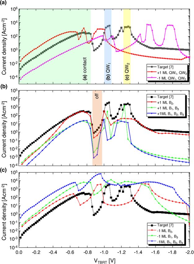
Journal of Physics D: Applied Physics
J. Phys. D: Appl. Phys. 54 (2021) 355104 (7pp) https://doi.org/10.1088/1361-6463/ac0a09
Simulations of resonant tunnelling
through InAs/AlSb heterostructures for
ULTRARAM™ memory
Dominic Lane∗ and Manus Hayne
Department of Physics, Lancaster University, Lancaster LA1 4YB, United Kingdom
E-mail: d.lane@lancaster.ac.uk
Received 19 April 2021, revised 25 May 2021
Accepted for publication 10 June 2021
Published 22 June 2021
Abstract
ULTRARAM™ is a III–V semiconductor memory technology which allows non-volatile logic
switching at ultra-low energy (per unit area). This is achieved by exploiting triple-barrier
resonant tunnelling (TBRT) through a series of InAs/AlSb heterojunctions specifically
engineered for this purpose. Electrons tunnelling through the barriers at low bias are trapped in
a floating gate, in which the presence or absence of charge defines the memory logic. Here, we
report detailed non-equilibrium Green’s functions simulations of the InAs/AlSb TBRT
heterostructure, which is the principal source of ULTRARAM™’s extraordinary performance
benefits. The effects of variations to the heterostructure layer thickness are investigated for
performance optimization, and for assessing growth and process tolerances for commercial
implementation on 12′′ Si wafers. Trade-offs between power, speed, logic disturbance and data
retention time are identified. Importantly, most one monolayer alterations to the tunnelling
region show the required characteristics for ULTRARAM™ memory operation, thus some
tolerance in any future commercial fabrication process is identified.
Keywords: compound semiconductor, resonant tunnelling, non-volatile memory (NVM),
non-volatile RAM (NVRAM), InAs/AlSb
(Some figures may appear in colour only in the online journal)
1. Introduction a small amount of energy. As the nature of these require-
ments appears antithetical, the widely accepted view is that
The development of a universal technology that replaces cur- universal memory is unfeasible [1] or almost impossible [2].
rent memory types has long been a major objective in the ULTRARAM™ is an emerging, floating-gate (FG) memory
semiconductor industry. A ‘universal memory’ should pos- technology that utilises the unique band offsets of the 6.1 Å
sess the speed of static random access memory, the non- semiconductor family (InAs, AlSb and GaSb) [3]. In par-
volatility, low-cost and high-density of flash and endurance of ticular, the non-volatility of the memory is derived from
dynamic random access memory. This necessitates a robust the extraordinarily large conduction band (CB) offset of
logic state which can nevertheless be easily changed with the InAs/AlSb heterojunction (2.1 eV), which plays a sim-
ilar role to the semiconductor-oxide barriers used in flash
∗
memories [4]. However, in ULTRARAM™, multiple ultrathin
Author to whom any correspondence should be addressed.
InAs/AlSb layers are used to form a triple-barrier resonant tun-
nelling (TBRT) structure between the channel and the FG [5].
Original content from this work may be used under the terms
of the Creative Commons Attribution 4.0 licence. Any fur-
This reconciles the contradictory requirements of a universal
ther distribution of this work must maintain attribution to the author(s) and the memory, as the tunnelling structure provides a 2.1 eV energy
title of the work, journal citation and DOI. barrier to retain memory logic, but allows resonant tunnelling
1361-6463/21/355104+7$33.00 1 © 2021 The Author(s). Published by IOP Publishing Ltd Printed in the UK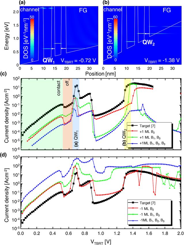
J. Phys. D: Appl. Phys. 54 (2021) 355104                                                                                     D Lane and M Hayne

of electrons (i.e. transparent barriers) at program/erase (P/E)
voltages less than 2.5 V, around 10 times lower than flash [6].
    The remarkable performance characteristics of
ULTRARAM™ are predicted by detailed simulations of
quantum transport [7], and encouraging results have been
demonstrated in single devices and 2 × 2 arrays at room
temperature on GaAs substrates at 20 µm gate lengths [8],
with implementation on Si substrates on-going [9]. Moreover,
recent experimental results validate our previous simulation
work, including the proposed half-voltage architecture for ran-
dom access memory (RAM) applications [10]. Our previous                 Figure 1. Device schematic for ULTRARAM™ memory as
                                                                        fabricated in [8–10], with Al2 O3 gate dielectric to prevent hole
theoretical investigations were for a specific layer thickness          leakage currents (not to scale). Material layers are presented
configuration of the triple-barrier InAs/AlSb tunnelling junc-          alongside with the TBRT region of particular interest to this work
tion [7]. In practice, growth of these layers with exact mono-          marked by a yellow arrow. Thicknesses of the TBRT layers are
layer (ML) precision is not straightforward. Indeed, thick-             given in table 1.
nesses could be offset across the entire growth due to imprecise
calibration, or vary across the wafer. This is of particular con-
                                                                                Table 1. Layer thicknesses of the TBRT region (Å).
cern for the commercial development of ULTRARAM™, as
it is vital that the InAs/AlSb heterostructures currently grown                                    B1       QW1       B2        QW2       B3
on 3′′ Si [9] be transferred onto 12′′ Si substrates in order to        Material                   AlSb     InAs      AlSb      InAs      AlSb
be cost-competitive. In this work, we present non-equilibrium
                                                                        Target [7]                  18       30        12        24        18
Green’s function (NEGF) simulations of the ULTRARAM™
                                                                        Equal QWs                   18       24        12        24        18
resonant tunnelling region, where layer thicknesses are varied          +1 ML QW1 , QW2             18       36        12        30        18
to investigate the effect on the performance of the memory.             −1 ML QW1 , QW2             18       24        12        18        18
Choices of layer alterations presented here are ±1 ML (i.e.             +1 ML B1 , B2 , B3          24       30        18        24        24
one lattice constant, 6 Å). It is possible for alterations of           −1 ML B1 , B2 , B3          12       30         6        24        12
0.5 ML to occur; however, these have a smaller impact on                +1 ML B1 , B3               24       30        12        24        24
the memory performance. Furthermore, the thinnest layer of              −1 ML B1 , B3               12       30        12        24        12
the tunnelling region has a target thickness of just 2 MLs              +1 ML B2                    18       30        18        24        18
(12 Å), so an increase of 2 MLs would represent a doubling              −1 ML B2                    18       30         6        24        18
in thickness, whilst a decrease of 2 MLs removes the layer              Channel and FG thicknesses are fixed to 120 Å. InAs and AlSb material
entirely.                                                               parameters can be found in the program database for nextnano. MSB and
                                                                        are fixed to experimental values [7, 13, 14].

2. Memory concept
                                                                        the memory [7, 12]. Consequently, this work will focus on
Logic switching of the memory state in ULTRARAM™ is                     the properties of charge retention and tunnelling of electrons
achieved via TBRT through the InAs/AlSb heterostructure.                between channel and FG only, with voltages (V TBRT ) given
Under an applied bias of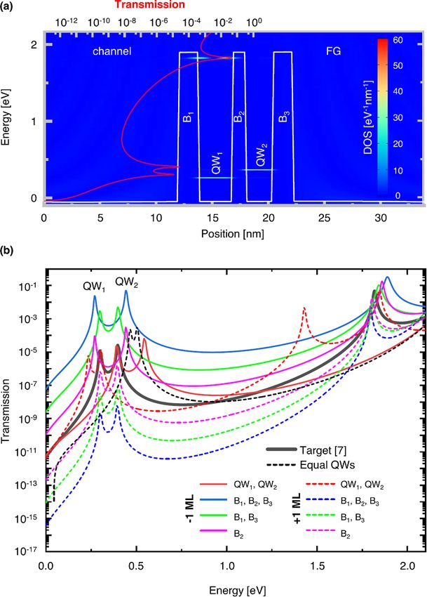
J. Phys. D: Appl. Phys. 54 (2021) 355104                                                                                      D Lane and M Hayne

3. Non-volatility

The ability of a memory to retain its logic state is important for
memory performance in both RAM and mass storage applic-
ations [16]. It has been predicted that the intrinsic (300 K)
storage time of electrons in the InAs/AlSb system exceeds the
age of the universe [17]. However, this prediction is based
on thermal excitation of electrons over the barrier potential.
To investigate the non-volatility of ULTRARAM™ we must
consider the effects of the TBRT structure on the transpar-
ency of the barriers. This is accomplished using NEGF sim-
ulations of the TBRT region at 300 K under zero applied bias.
The simulation results detailed here are modelled using next-
nano multi-scattering Büttiker (MSB) software, the details of
which can be found in [7, 13]. Figure 2(a) shows the calcu-
lated CB edge (white) for the target TBRT structure, where
the barriers and wells are labelled in accordance with table 1.
The colour scale of the density of states (DOS) demonstrates
the confinement energies of the QWs (QW1 and QW2 ). The
transmission function, T, i.e. the likelihood of electrons leav-
ing or entering the FG, is shown by the red line (log-scale).
It is extremely small in the energy region below the barrier
height; however, it possesses three distinct points of interest.
The first is a transmission peak corresponding to the resonant
state of the QW1 ground state, the second is the transmission
peak for the QW2 ground state, and, finally, the largest trans-
mission peak is for the second confined state of QW1 . Note that
for the target TBRT structure in figure 2, QW2 is too narrow
to have a second confined QW state. The largest transmission
peak of T = 0.04 resides at an energy (E) of around 1.8 eV,
which corresponds to an electron storage time of about 1010                 Figure 2. NEGF transmission calculations for the ULTRARAM™
years at room temperature [17]. The lower energy (QW1 and                   TBRT region at 300 K under zero bias. (a) Position-resolved,
                                                                            electron energy levels of the QWs for the target heterostructure,
QW2 ) transmission peaks are at T ∼ 10−5 , E = 0.29 eV and at               where the colour-scale indicates the DOS. The conduction band
T ∼ 10−5 , E = 0.4 eV, respectively. Although the peaks reside              calculation is shown by the white line. The corresponding
at a much lower energy, corresponding to millisecond stor-                  transmission function (red line) demonstrates the peak alignments
age times at room temperature for localization energies of that             with the confined energy levels in the structure. (b) Transmission
size [17], the probability of transmission is very low, making it           functions for each layer thickness alteration described in table 1.
                                                                            Results are described in detail in the text.
unlikely that these peaks impact on the retention capability of
the memory. Indeed, fabricated devices show stable memory
retention exceeding 24 h at 300 K with little or no state decay
[8, 10].                                                                    with QW2 becomes coincident with that of QW1 in the tar-
    Monolayer alterations to the target structure are assessed by           get structure, in both cases corresponding to a QW thickness
repeating the NEGF calculations under the same conditions for               of 30 Å, and the peak associated with QW1 moves to lower
each of the alterations listed in table 1. The results for the trans-       energy. The 1 ML increase also shifts the transmission peak
mission function are presented in figure 2(b). Alterations to the           associated with the second confined state of QW1 to lower
QW thicknesses shifts the ground states of the QWs. A 1 ML                  energy, and introduces a new peak associated with the second
reduction in QW thickness shifts the start of the QW1 trans-                confinement energy of QW2 at similar energy and transmis-
mission peak to a higher energy (solid red line, figure 2(b))               sion to the second confined state of QW1 in the target structure.
by around 100 meV, with similar transmission, such that it is               Overall, with barriers at the target widths, the energies and
coincident with the transmission peak associated with QW2 in                magnitudes of the transmission peaks are closely associated
the target structure. This is not unexpected as the QW width                with given QW widths, and somewhat independent of each
in both cases is the same. In the same way, the transmission                other. If QW thicknesses are equal, the increased overlap inter-
peak associated with QW2 shifts to higher energy. The result                action between the wells increases transmission by an order of
would be an improvement in retention compared to the target                 magnitude, as shown in figure 2(b) (black dashed line).
structure. The converse argument can be made for increasing                    Reducing the thickness of the barriers increases the trans-
QW thicknesses by 1 ML (dotted red line, figure 2(b)), which                mission probabilities. A 1 ML thickness reduction of all barri-
would decrease retention. The transmission peak associated                  ers increases the transmission probability at the QW1 ground

                                                                        3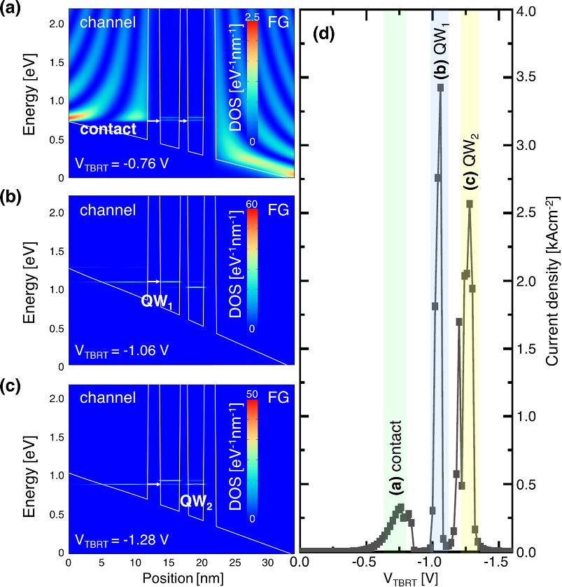
J. Phys. D: Appl. Phys. 54 (2021) 355104                                                                                  D Lane and M Hayne

state energy by about three orders of magnitude to T = 0.02,
with a consequential detrimental impact on the non-volatility
of the memory (solid blue line, figure 2(b)). Reducing the
thickness of the central barrier (B2 ) results in greater separa-
tion between QW1 and QW2 peak energies as the energy split-
ting effect from the interaction of the two QW ground states
due to the Pauli exclusion principle is increased [18]. This
pushes the QW1 energy lower which could negatively impact
retention, however the transmission remains relatively small
(solid pink line, figure 2(b)). Unsurprisingly, increasing the
barrier thicknesses has the opposite effect, and will result in
improved retention capability of ULTRARAM™ if required
(dotted blue, green and pink lines, figure 2(b)), with success-
ive 1 ML increases in barrier thickness each delivering a reduc-
tion in QW peak transmission of about an order of magnitude.
There will be a trade-off between the resonant-tunnelling cur-
rent characteristics and the charge-blocking properties, so we
cannot yet conclude that thickening the barriers is a super-
ior design choice for the technology until the full extent of
ULTRARAM™ retention properties have been investigated
experimentally. Crucially, we find that the retention of the
memory should not be detrimentally impacted by most 1 ML
alterations, with the main retention concerns being the cases
                                                                        Figure 3. Simulations of the target TBRT junction for the memory
where thickness is reduced for all barriers. Fortunately, the           (300 K) for tunnelling of the program cycle. (a) DOS of states for
latter scenario is experimentally relatively unlikely, as it rep-       the ‘leads’ (contacts) under bias corresponding to the contact peak
resents a large change in percentage error in layer thickness           of the current density plot. (b) DOS (colour scale) plot for the
for layers grown in close proximity to each other. This is a            tunnelling voltage of QW1 current density peak. (c) DOS (colour
promising result regarding the commercial implementation of             scale) plot for the tunnelling voltage of QW2 current density peak.
                                                                        (d) Current density plot of the TBRT region as a function of applied
ULTRARAM™, but demonstrates that process and growth                     bias. Labelled peaks correspond to the resonant energy alignments
tolerances are of paramount importance.                                 of (a)–(c).

4. Tunnelling current                                                   electric field, the sloping of the CB forms a triangular quantum
                                                                        potential well at the channel-B1 interface such that resonant
The TBRT mechanism used to program (i.e. add electrons to               tunnelling through the structure is a 2D-2D process with a con-
the FG) for ULTRARAM™ memory devices is demonstrated                    centrated DOS. Here, electrons occupy the triangular quasi-
in figure 3, where all calculations are again carried out using         bound state due to inelastic scattering. Without the inclusion
the nextnano MSB software package [13]. Resonant tunnel-                of inelastic scattering the device operates in an entirely differ-
ling occurs under the condition that the energy of electrons            ent way whereby the current-density characteristic is entirely
in the channel align with the available energies of the TBRT            determined by the properties of the lead (contact), rather than
structure (i.e. the QW1 or QW2 ground state energies). This is          by details of the CB in the device [20]. Two large tunnelling
measured as a current density through the barriers, as shown            current density peaks emerge corresponding to alignment with
in figure 3(d), containing three distinct peaks. The DOS plots          the QW1 and QW2 ground states at V TBRT = −1.06 V and
under applied bias reveal the resonant conditions of the large          V TBRT = −1.28 V, respectively. Tunnelling through the QW2
tunnelling currents (figures 3(a)–(c)) as labelled on the cur-          state can occur despite the QW1 state residing at higher energy
rent density plot. The low-voltage peak (figure 3(a)) occurs            due to the wave-function overlap between the QWs, which can
when the electron energies from the contact align with the              be seen in the DOS plots of figure 3(c).
QW ground states, producing a broad peak. However, if we                   When interpreting a resonant tunnelling current-density
turn our attention to the device construction shown in figure 1,        plot for the purposes of ULTRARAM™ memory there are
the channel is such that the contact is spatially separated from        important properties to consider. First, there is the magnitude
the gate stack, therefore resonant tunnelling directly from the         of the current density peaks, which is directly related to
contact (i.e. ballistic tunnelling that bypasses the InAs CB            the device switching speed [7], where larger current peaks
entirely) is not possible. We conclude that this is not part            improve performance. Second is the voltage (V TBRT ) at which
of the ULTRARAM™ tunnelling mechanism and is an arte-                   the peak occurs; a high voltage will consume more power,
fact of the simulation construction. Indeed, experimental stud-         whilst a very small voltage is more likely to have logic dis-
ies support this assertion [8–10, 19]. The peaks occurring at           turbances under readout biasing. Lastly, is the sharpness of
higher voltages are the expected resonant tunnelling peaks              the onset of the peaks; a significant tunnelling current away
(figures 3(b) and (c)). As the TBRT region is under a large             from the P/E peak voltage will also cause logic disturbances

                                                                    4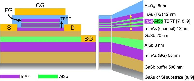
J. Phys. D: Appl. Phys. 54 (2021) 355104                                                                                       D Lane and M Hayne

                                                                               retention as discussed in the previous section. It is worth
                                                                               noting that this speed reduction may be significant, but it
                                                                               is likely that ULTRARAM™ would still outperform current
                                                                               memory technologies as the tunnelling mechanism is intrins-
                                                                               ically fast [7, 8, 21]. Increasing the thickness of the middle
                                                                               barrier (red dots, figure 4(b)) greatly reduces the tunnelling
                                                                               current from QW2 (compared to QW1 ) due to the reduction
                                                                               in wave-function overlap between the QWs, with the ground
                                                                               state of QW1 above the energy QW2 (similar to figure 3(c)).
                                                                               Logic disturbances at low voltages within the architecture can
                                                                               be evaluated from the region below the peak, depicted by the
                                                                               orange shading in figure 4(b), where we ignore tunnelling from
                                                                               the contact for reasons previously discussed (labelled ‘off’).
                                                                               Increasing barrier thickness reduces the current density in the
                                                                               off region which could be used to reduce logic disturbance.
                                                                               However, it should be noted here that testing on fabricated
                                                                               devices retained robust logic states after 105 disturbance cycles
                                                                               [8, 10].
                                                                                   Reducing the barrier thicknesses increases the current dens-
                                                                               ities, as shown in figure 4(c). However, the maximum increase
                                                                               from these alterations is just over one order of magnitude, so
                                                                               switching speed benefits must be carefully weighed against
                                                                               other requirements of the memory. Decreasing the thickness
                                                                               of the outer barriers, B1 and B3 , slightly increases the current-
                                                                               density (figure 4(c), green triangles), but broadens the peaks
                                                                               and produces a more gradual ramp to peak current (with omit-
                                                                               ted contact tunnelling i.e. the in the off region). This could
                                                                               negatively impact logic disturbance, both during readout and
                                                                               for the unique half-voltage RAM architecture [7, 10], as well
Figure 4. Nextnano MSB NEGF simulations (300 K) of TBRT                        as retention ability. Reducing the thickness of the middle bar-
current density for the program cycle for each of the alterations              rier causes energy splitting of the two QW ground states [18],
listed in table 1. Results are described in detail in the text. (a) 1 ML
                                                                               which results in the QW1 peak moving to a lower voltage
alterations to the QWs. (b) Increased barrier thicknesses.
(c) Decreased barrier thicknesses.                                             requirement and the QW2 peak moving to a higher voltage
                                                                               (figure 4(c), red dots). There are no obvious disadvantages
                                                                               to this configuration, and the energy shift in QW1 could be
[7]. It can be seen in figure 3 that the resonant tunnelling cur-              used for lower voltage memory operation using a single peak
rent forms sharp peaks at a little over 1 V, indicating that the               for the resonant-tunnelling current density. Reducing all bar-
TBRT structure is highly suitable for the implementation of                    rier thicknesses results in a much broader current density rela-
FG memory, as demonstrated in experimental work to date                        tion, where it is likely that any gains in switching speed are
[5, 8–10]. The simulations are repeated under the same condi-                  outweighed by the degradation of other memory perform-
tions for each of the structures listed in table 1 for the program             ance aspects. Most alterations possess desirable P cycle tun-
cycle, and are shown in figure 4. Alterations to the QW thick-                 nelling characteristics for ULTRARAM™ operation, which
nesses (figure 4(a)) shift their ground state energies such that               is positive for the purposes of production wafer tolerances.
a reduction in thickness increases the required electric field                 The performance trade-offs in the design have been identified,
for resonant tunnelling alignments (pink triangles, figure 4(a)).              however, decisions on this should be informed after a more
Moreover, this shift outweighs the increase in electric field                  extensive experimental investigation of the target design.
caused by thinning the structure. The converse applies when                        The simulations are repeated with a reversed tunnelling bias
thickening the QWs. The magnitude of the current density                       (V TBRT ) to investigate the erase cycle of the memory (remov-
peaks is not significantly affected. Thus, changes to the QW                   ing electrons from the FG). The current-density peaks which
thicknesses could serve as a valuable method in tuning the                     move electrons out of the FG occur at energy alignments with
memory for operation at a desired voltage without hindering                    the QW1 and QW2 ground states in a similar fashion to the
performance.                                                                   P cycle. This is demonstrated in figures 5(a) and (b), where
   Figure 4(b) presents the results of thickening barrier lay-                 the QW DOS alignments in the target structure correspond to
ers on the P cycle current density. Increasing barrier thick-                  the peaks as labelled in the current density plot (figure 5(c),
ness reduces the current density by up to two orders of                        black squares). Increasing the barrier thicknesses reduces the
magnitude, which could degrade the speed of the memory.                        magnitude of the current density peaks (figure 5(c)). Increas-
However, a trade-off could be made with the retention cap-                     ing the thickness of all the barriers or the outer barriers
ability such that speed is exchanged for more robust logic                     (figure 5(c) green and blue triangles, respectively) reduces

                                                                           5
J. Phys. D: Appl. Phys. 54 (2021) 355104 D Lane and M Hayne
However, these benefits should be carefully weighed against a
potentially reduced retention capability and consequences of
split P cycle tunnelling peaks, as previously discussed.
5. Conclusions
The InAs/AlSb TBRT region which forms the basis of the
ULTRARAM™ memory concept has been investigated in
detail using the nextnano.MSB software package (NEGF with
Büttiker probe scattering) to determine memory performance
characteristics. Monolayer alterations are made to the tunnel-
ling structure with the aim of realizing the optimum choice
of layer structure whilst considering the growth tolerances
required of a commercially-produced wafer. Transmission
function calculations indicate that most monolayer alterations
have a minimal effect on the retention capabilities. Thicken-
ing the barriers reduces low-energy transmission, improving
retention, whilst the thinnest barrier configuration investig-
ated allows 0.02 transmission atJ. Phys. D: Appl. Phys. 54 (2021) 355104 D Lane and M Hayne
Manufacturing Hub Grant EP/P006973/, by the ATTRACT Electron Devices Technology & Manufacturing Conf.
project funded by the EC under Grant Agreement 777222 and (EDTM) (Chengdu) (https://doi.org/10.1109/EDTM
by the Joy Welch Educational Charitable Trust. 50988.2021.9420825)
[11] Chou H Y, O’Connor E, O’Mahony A, Povey I M, Hurley P K,
Dong L, Ye P D, Afanas’ev V V, Houssa M and Stesmans A
2016 Band offsets and trap-related electron transitions at
ORCID iD interfaces of (100)InAs with atomic-layer deposited Al2 O3
J. App. Phys. 120 235701
Dominic Lane https://orcid.org/0000-0001-6647-2869 [12] Kolodny A, Nieh S T K, Eitan B and Shappir J 1986 Analysis
and modeling of floating-gate EEPROM cells IEEE Trans.
Electron Devices 33 835
References [13] Birner S Web site of nextnano GmbH company (available at:
www.nextnano.de)
[1] Wong H S and Salahuddin S 2015 Memory leads the way to [14] Li Y et al 2011 Electron mobility in modulation-doped
better computing Nat. Nanotechnol. 10 191 AlSb/InAs quantum wells J. Appl. Phys. 109 073703
[2] Yu S and Chen P 2016 Emerging memory technologies: recent [15] Shinohara K, Shimizu Y, Shimomura S and Hiyamizu S 1999
trends and prospects IEEE Solid-State Circuits Mag. GaAs/Al0.4Ga0.6As triple barrier resonant tunneling
2 43 diodes with (4 1 1)A super-flat interfaces grown by MBE J.
[3] Vurgaftman I et al 2001 Band parameters for III–V compound Cryst. Growth 201 773
semiconductors and their alloys J. Appl. Phys. [16] Bez R and Pirovano A 2004 Non-volatile memory
89 5815 technologies: emerging concepts and new materials Mater.
[4] Pavan P, Bez R, Olivo P and Zanoni E 1997 Flash memory Sci. Semicond. Process. 7 349
cells-an overview Proc. IEEE 85 1248 [17] Nowozin T, Bimberg D, Daqrouq K, Ajour M N and Awedh M
[5] Tizno O, Marshall A R J, Fernández-Delgado N, Herrera M, 2013 Materials for future quantum dot-based memories J.
Molina S I and Hayne M 2019 Room-temperature operation Nanomater. 2013 215613
of low-voltage, non-volatile, compound-semiconductor [18] Harrison P and Valavanis A 2016 Quantum Wells, Wires and
memory cells Sci. Rep. 9 8950 Dots: Theoretical and Computational Physics of
[6] Prall K 2017 Benchmarking and metrics for emerging memory Semiconductor Nanostructures 4th edn (New York: Wiley)
2017 IEEE Int. Memory Workshop (Monterey) p 163
pp 1–5 [19] Hwang H P et al 1994 High peak-to-valley current ratio In/sub
[7] Lane D and Hayne M 2020 Simulations of ultralow-power 0.3/Ga/sub 0.7/As/In/sub 0.29/Al/sub 0.71/As resonant
nonvolatile cells for random-access IEEE Trans. Electron tunneling diodes grown on GaAs 1994 Int. Electron
Devices 67 474 Devices and Materials Symp. (EDMS) (Hsinchu, Taiwan)
[8] Lane D, Hodgson P D, Potter R J, Beanland R and Hayne M p3
2021 ULTRARAM: toward the development of a III–V [20] Kubis T 2009 Quantum transport in semiconductor
semiconductor, nonvolatile, random access memory IEEE nanostructures PhD Thesis Technische Universität München
Trans. Electron Devices 68 2271 [21] Feiginov M 2019 Frequency limitations of resonant-tunnelling
[9] Hodgson P D, Hodgson P D, Sen N and Das S 2021 III–V diodes in sub-THz and THz oscillators and detector J.
non-volatile ULTRARAM™ memory on Si 2021 APL Infrared Millim. Terahz. Waves 40 365
Materials: Materials Challenges for Memory (Mcfm), [22] Lane D and Hayne M Simulations of resonant tunneling
Virtual Conf. vol 37 pp 3038–48 through InAs/AlSb heterostructures for ULTRARAM™
[10] Lane D et al 2021 Demonstration of a fast, low-voltage, III–V memory (dataset) (https://doi.org/10.17635/
semiconductor, non-volatile memory 2021 5th IEEE lancaster/researchdata/467)
7You can also read