Datasheet UFS Spec v3.1 Compliant UniPro Spec v1.8 Compliant M-PHY Spec v4.1 Compliant
←
→
Page content transcription
If your browser does not render page correctly, please read the page content below
Datasheet
UFS 3.1 Total IPTM
                                                            UFS Spec v3.1 Compliant
                                                          UniPro Spec v1.8 Compliant
                                                          M-PHY Spec v4.1 Compliant

Arasan Chip Systems Inc.
2150 North First Street, Suite #240, San Jose, CA 95131
Ph: 408-433-9633
Fax: 408-282-7800
www.arasan.com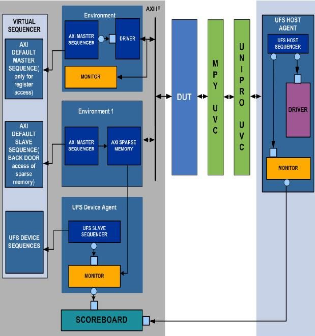
Datasheet

Disclaimer
This document is written in good faith with the intent to assist the readers in the use of the product.
Circuit diagrams and other information relating to Arasan Chip Systems’ products are included as a
means of illustrating typical applications. Although the information has been checked and is believed to
be accurate, no responsibility is assumed for inaccuracies. Information contained in this document is
subject to continuous improvement and development.

Arasan Chip Systems’ products are not designed, intended, authorized or warranted for use in any life
support or other application where product failure could cause or contribute to personal injury or
severe property damage. Any and all such uses without prior written approval of an Officer of Arasan
Chip Systems Inc. will be fully at the risk of the customer.

Arasan Chip Systems Inc. disclaims and excludes any and all warranties, including, without limitation,
any and all implied warranties of merchantability, fitness for a particular purpose, title, and infringement
and the like, and any and all warranties arising from any course or dealing or usage of trade.

This document may not be copied, reproduced, or transmitted to others in any manner. Nor may any
use of information in this document be made, except for the specific purposes for which it is transmitted
to the recipient, without the prior written consent of Arasan Chip Systems Inc. This specification is
subject to change at any time without notice. Arasan Chip Systems Inc. is not responsible for any errors
contained herein.

In no event shall Arasan Chip Systems Inc. be liable for any direct, indirect, incidental, special, punitive,
or consequential damages; or for loss of data, profits, savings or revenues of any kind; regardless of the
form of action, whether based on contract; tort; negligence of Arasan Chip Systems Inc or others; strict
liability; breach of warranty; or otherwise; whether or not any remedy of buyers is held to have failed of
its essential purpose, and whether or not Arasan Chip Systems Inc. has been advised of the possibility of
such damages.

Restricted Rights
Use, duplication, or disclosure by the Government is subject to restrictions as set forth in FAR52.227-14
and DFAR252.227-7013 et seq. or its successor.

Copyright Notice
No part of this specification may be reproduced in any form or means, without the prior written consent
of Arasan Chip Systems, Inc.

Questions or comments may be directed to:

Arasan Chip Systems Inc.
2150 North First Street, Suite 240
San Jose, CA 95131
Ph: 408-282-1600
Fax: 408-282-7800
Email: sales@arasan.com

 Copyright © 2021, Arasan Chip Systems Inc.
Datasheet

Contents
1      Introduction ........................................................................................................ 1
    1.1      About UFS Standard ......................................................................................................... 1
    1.2      Arasan’s Contribution to MIPI .......................................................................................... 1
    1.3      Arasan’s Total IPTM Solution ............................................................................................. 1

2      UFS 3.1 Host IP .................................................................................................... 3
    2.1 Overview .......................................................................................................................... 3
    2.2 Features ............................................................................................................................ 3
    2.3 Architecture...................................................................................................................... 4
      2.3.1 Functional Description................................................................................................ 4
      2.3.2 Functional Block Diagram ........................................................................................... 4
      2.3.3 Functional Block Diagram Description ........................................................................ 5
    2.4 PIN Diagram...................................................................................................................... 7
    2.5 IP Deliverables .................................................................................................................. 8
3      UFS 3.1 Device IP ................................................................................................ 9
    3.1 Features ............................................................................................................................ 9
    3.2 Architecture...................................................................................................................... 9
      3.2.1  Functional Description................................................................................................ 9
      3.2.2  Functional Block Diagram ......................................................................................... 10
      3.2.3  Functional Block Diagram Description ...................................................................... 10
    3.3 PIN Diagram.................................................................................................................... 12
    3.4 Soc Level Integration ...................................................................................................... 13
      3.4.1  IP Deliverables.......................................................................................................... 13
      3.4.2  Verification Environment.......................................................................................... 13

4      UniPro 1.8 .........................................................................................................15
    4.1 Overview ........................................................................................................................ 15
    4.2 Features .......................................................................................................................... 15
    4.3 UniPro System Bus ......................................................................................................... 15
    4.4 Architecture.................................................................................................................... 16
      4.4.1  Functional Block Diagram ......................................................................................... 16
      4.4.2  Functional Block Diagram Description ...................................................................... 16
    4.5 PIN Diagram.................................................................................................................... 18
    4.6 Configurable Features .................................................................................................... 19
    4.7 Deliverables .................................................................................................................... 19

5      M-PHY 4.1 .........................................................................................................20
    5.1      Overview ........................................................................................................................ 20

 Copyright © 2021, Arasan Chip Systems Inc.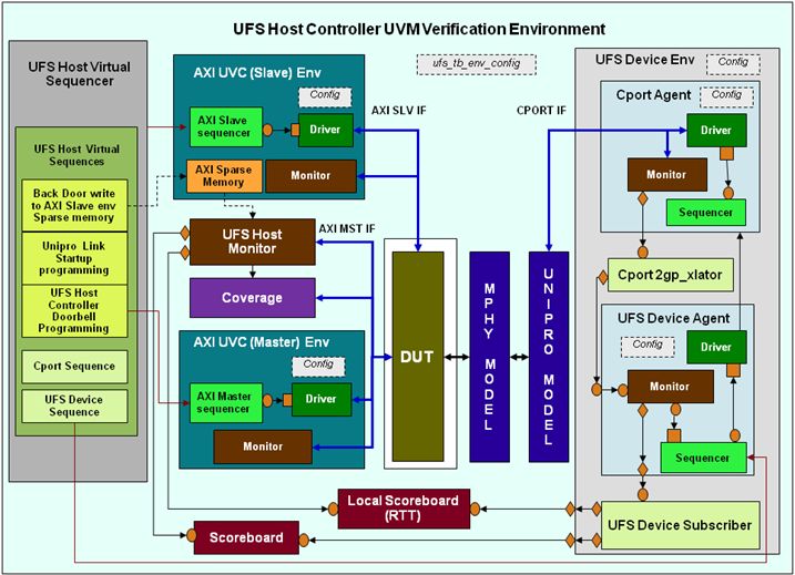
Datasheet

      5.1.1 Lanes ........................................................................................................................ 20
      5.1.2 Signaling ................................................................................................................... 20
      5.1.3 Line Coding .............................................................................................................. 20
      5.1.4 M-PHY Type ............................................................................................................. 21
    5.2 Overview of Arasan M-PHY for UFS ............................................................................... 21
    5.3 Arasan’s M-PHY for UFS Features .................................................................................. 21
    5.4 M-PHY Pad Table ............................................................................................................ 23
      5.4.1 Functional Description of M-PHY Pads for Tx Lane .................................................... 23
      5.4.2 Functional Description of M-PHY Pads for Rx Lane ................................................... 23
      5.4.3 UFS Specific Pins ....................................................................................................... 23
      5.4.4 Protocol Interface (PIF) Signals ................................................................................. 23
    5.5 Power Pads ..................................................................................................................... 27
      5.5.1 Analog Configuration Bit (Trim Bits).......................................................................... 27
    5.6 Hard Macro Deliverables................................................................................................ 27
6      UFS 3.1 Software Stack & Driver .......................................................................29
    6.1      Overview ........................................................................................................................ 29
    6.2      Features .......................................................................................................................... 29
    6.3      Architecture.................................................................................................................... 29
    6.4      Deliverbles ...................................................................................................................... 30
7      UFS 3.1 Hardware Validation Platform .............................................................31
    7.1      Overview ........................................................................................................................ 31
    7.2      Features .......................................................................................................................... 31
    7.3      Description ..................................................................................................................... 31
    7.4      Deliverables .................................................................................................................... 32

8      UFS Verification IP (VIP) ....................................................................................33
    8.1 UVM Verification Environment ...................................................................................... 33
      8.1.1  UVM Verification Environment Components ............................................................ 34
      8.1.2  UFS Host UVM Model ............................................................................................... 35
      8.1.3  UFS Device UVM Model............................................................................................ 36
      8.1.4  Verification Deliverables........................................................................................... 37
    8.2 Verilog Verification Environment ................................................................................... 38
      8.2.1  Generator ................................................................................................................ 38
      8.2.2  Scoreboard ............................................................................................................... 38
      8.2.3  AHB Master Model ................................................................................................... 38
      8.2.4  AXI Slave Model ....................................................................................................... 39
      8.2.5  UniPro Function Model ............................................................................................ 39
      8.2.6  MPHY Function Model .............................................................................................. 39
      8.2.7  DUT .......................................................................................................................... 39

 Copyright © 2021, Arasan Chip Systems Inc.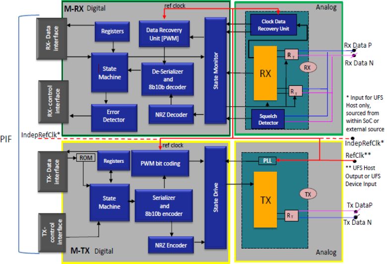
Datasheet
9 Services & Support ............................................................................................41
9.1 Global Support ............................................................................................................... 41
9.2 Arasan Support Team ..................................................................................................... 41
9.3 Professional Services & Customization .......................................................................... 41
9.4 The Arasan Porting Engine ............................................................................................. 41
9.5 Pricing & Licensing.......................................................................................................... 41
Tables
Table 1: UniPro Features and Compile Time Options ...................................................................... 19
Table 2: UniPro Features and Run Time Options ............................................................................. 19
Table 3: Functional description of M-PHY Pads for Tx lane.............................................................. 23
Table 4: Functional Description of M-PHY Pads for Rx Lane ............................................................ 23
Table 5: UFS Specific Pins ............................................................................................................... 23
Table 6: M-TX-CTRL Signals ............................................................................................................. 23
Table 7: M-TX Data Transfer Signals ............................................................................................... 24
Table 8: M-RX CTRL Interface Signals .............................................................................................. 25
Table 9: M-RX Data Interface Signals .............................................................................................. 26
Table 10: Power Pads ..................................................................................................................... 27
Table 11: Ports for trim_bits ........................................................................................................... 27
Figures
Figure 1: Arasan's Total IP Solution ................................................................................................... 2
Figure 2: UFS Host Controller Functional Block Diagram ................................................................... 4
Figure 3 : UFS Host IP Pinout Diagram .............................................................................................. 7
Figure 4 UFS Device Controller Functional Block Diagram ............................................................... 10
Figure 5: UFS Device IP Pinout Diagram .......................................................................................... 12
Figure 6: UFS Device IP – Verification Environment ........................................................................ 14
Figure 7: UniPro Controller Architecture Block Diagram ................................................................. 16
Figure 8: UniPro IP Pinout Diagram ................................................................................................. 18
Figure 9: Illustration of MIPI M-PHY Link ........................................................................................ 20
Figure 10: M-PHY Type1 and Type 2 Module .................................................................................. 21
Figure 11: ACS M-PHY for UFS Block Diagram ................................................................................. 22
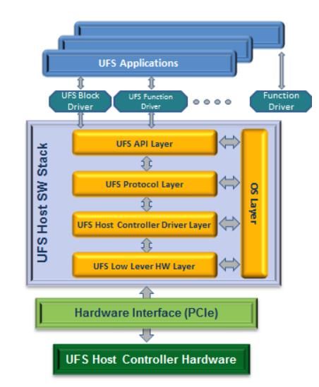
Figure 12: UFS Host Stack Architecture ........................................................................................... 30
Figure 13: UFS HVP Architecture..................................................................................................... 32
Figure 14: UFS Verification Environment Diagram .......................................................................... 33
Figure 15: UFS Host UVM Environment .......................................................................................... 36
Figure 16: UFS Host UVM Environment .......................................................................................... 37
Figure 17: UFS Host Verilog Environment ....................................................................................... 38
Copyright © 2021, Arasan Chip Systems Inc.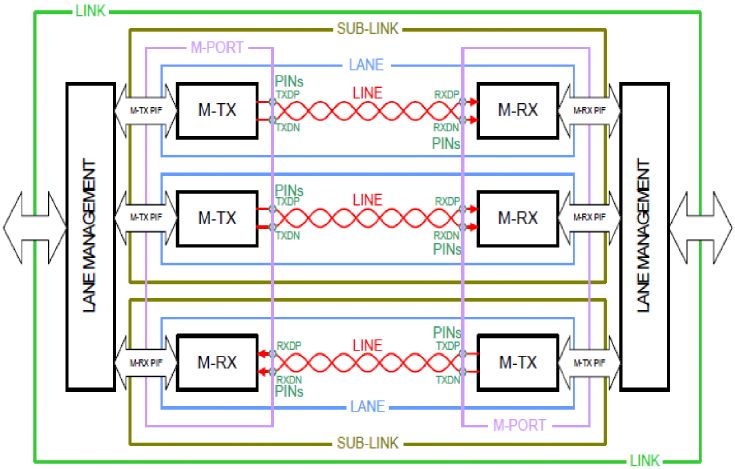
Datasheet

 Copyright © 2021, Arasan Chip Systems Inc.
Datasheet
1 Introduction
1.1 About UFS Standard
UFS (Universal Flash Storage) is a high-performance storage interface, designed for use in
computing and mobile systems, requiring low power consumption such as smart phones and
tablets. Its high-speed serial interface and optimized SCSI protocol enable significant improvements
in throughput and system performance. UFS v3.1 defines bandwidth of up to 1.2 GB/s over two
data lanes.
The UFS standard has been developed and published by JEDEC™ Solid State Technology Association
(www.jedec.org), the global leader in the development of standards for the microelectronics
industry. JEDEC has over 4,000 participants, representing nearly 300 companies, working together
in 50 JEDEC committees.
1.2 Arasan’s Contribution to MIPI
Arasan Chip Systems has been an executive / contributing member with the UFSA since its inception
in 2010. Before that, Arasan has been, and still is, a contributor to the eMMC standard, the
predecessor for UFS, since 2001.
Arasan is the leader of mobile storage, with 300 IP licensees for SD /SDIO, ONFI Compliant NAND,
eMMC and UFS. Our UFS Host and Device IPs were licensed to both Application Processor
companies like Qualcomm, LG and Samsung, as well as the majority of the Memory companies, and
includes Samsung, Micron, SK Hynix, among others.
Arasan’s active involvement and contribution to the relevant standards bodies, lead to deep
domain expertise, which in turn results in early availability of high-quality standards compliant IP for
our customers.
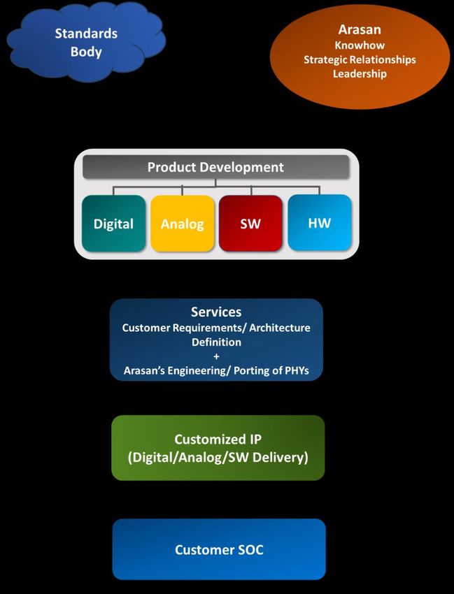
1.3 Arasan’s Total IPTM Solution
Arasan provides a Total IPTM Solution, which encompasses all aspects of IP development and
integration, including analog and digital IP cores, verification IP, software stacks & drivers, and
hardware validation platforms. Benefits of Total IPTM Solution:
• Seamless integration from PHY to Software
• Assured compliance across all components
• Single point of support
• Easiest acquisition process (one licensing source)
• Lowest overall cost including cost of integration
• Lowest risk for fast time to market
Copyright © 2021, Arasan Chip Systems Inc. 1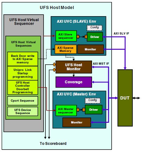
Datasheet

                                   Figure 1: Arasan's Total IPTM Solution

 Copyright © 2021, Arasan Chip Systems Inc.                                 2
Datasheet
2 UFS 3.1 Host IP
2.1 Overview
Universal Flash Storage (UFS) is a JEDEC standard for high performance mobile storage devices
suitable for next generation data storage. UFS is also adopted by Mobile Industry Processor
Interface (MIPI) as a data transfer standard designed for mobile systems. UFS incorporates the MIPI
UniPro standard as well as the MIPI Alliance M-PHY standard. Most UFS applications require large
storage capacity for data and boot code. Applications include mobile phones, tablets, Digital Still
Camera (DSC), Portable Media Player (PMP), MP3, and other applications requiring mass storage,
boot storage, XIP or external cards. The UFS standard is a simple but high-performance serial
interface that efficiently moves data between a host processor and mass storage devices. USF
transfers follow the SCSI model, but with a subset of Small Computer System Interface (SCSI)
commands. The Arasan UFS IP family consists of Host controller IP, Device controller IP, and M-PHY.
The UFS compliant IP cores are interface building blocks that simplify interconnect architectures in
mobile platforms. This leads to smaller footprint, greater interoperability between mobile IP, chips
and devices from diverse sources, and lower power and Electro Magnetic Interface (EMI).
Arasan’s UFS Host Controller IP, described in this document, is designed for ease of integration,
highest interoperability, and fully compliant to the JEDEC standards. It is implemented based on
Arasan’s proven MIPI technology, including UniPro and M-PHY.
The UFS 3.1 specification adds HS-GEAR3 and HS-GEAR4 as mandatory. The UniPro 1.8 specification
adds new attributes and modified some of the existing attributes for each layer.
2.2 Features
• Compliant with the following specification versions:
JESD220E UFS 3.1
JESD223D UFS 3.0 Host Controller Interface (HCI)
MIPI UniPro version 1.8
MIPI M-PHY version 4.1
• Interfaces Supported:
AXI Bus Protocol (AXI)
Advanced High-Performance Bus (AHB), Open Core Protocol (OCP) (Optional)
High-performance M-PHY type 1
• Core Features:
Two Lanes
Low power with multiple power operating modes
Configurable Transmit and Receive First In First Out (FIFO)s
Copyright © 2021, Arasan Chip Systems Inc. 3Datasheet
• Error Detection and Reporting:
Supports data and task management
Supports for multiple commands and tasks
• UFS 3.1:
Deep Sleep Power mode
Host Performance Booster (HPB)
Write Booster
2.3 Architecture
2.3.1 Functional Description
The UFS uses UniPro as the Datalink Layer. UniPro only supports point-to-point links as these
require the highest data rates required by the devices. The principal components of the UFS Host
UniPro IP are AXI Interface, UFS Host Controller Interface, UFS Transport Protocol Layer (UTP),
Transport Layer, Network Layer, Data Link Layer, PHY Adapter Layer and M-PHY.
2.3.2 Functional Block Diagram
Figure 2: UFS Host Controller Functional Block Diagram
Copyright © 2021, Arasan Chip Systems Inc. 4Datasheet
2.3.3 Functional Block Diagram Description
2.3.3.1 PHY Adapter Layer (L1.5)
• Link initialization, Power management, Hibernation, PACP frame handling to Get/Set any
feature at local or peer end
• Interface with M-PHY (Type I) to Send /Receive frames across physical lane
• Skip the Symbol insertion to reduce protocol payload bandwidth at the transmitter in order to
compensate for symbol interval tolerances between fast transmitter and slow receivers
• Data Scrambling is used to mitigate problems related to Electromagnetic Interference
• Max up to HS-G4 Support:
Single Lane and Two Lanes operation support
Lane Management for Two Lanes operation
2.3.3.2 Data Link Layer (L2)
The main responsibilities of Data Link Layer are to provide link between a transmitter and a
receiver, and to multiplex and arbitrate multiple types of data traffic. The Data Link Layer clusters
the PHY Adapter Protocol Data Units’ (PA-PDU’s) 17-bit symbols into data frames. Every data frame
consists of a 1-symbol header, L2 Payload, and a 2-symbol trailer incorporating a checksum (CRC-
16). Payloads with uneven number of bytes are extended with an extra padding byte and the
existence of the padding byte is flagged in the frame’s trailer. Control frames are also available
other than data frames. The control frames do not contain application data, and this allows both
ends of a link to communicate with each other to provide flow control and to handle transmission
of errors.
2.3.3.3 Network Layer (L3)
The purpose of the Network Layer is to allow data to be routed to the proper destination in a
network environment. A source device is responsible for supplying the address of the destination
device it wants to communicate.
2.3.3.4 Transport Layer (L4)
The Transport Layer is the highest protocol layer covered by UniPro. The Transport Layer supports
multiple bidirectional connections between the endpoint devices. UniPro guarantees that data sent
over a single connection arrive in the same order in which it was sent. All data sent over a single
connection has the same Traffic Class number (TC0). The Protocol Data Units (PDU’s) of the
Transport Layer are called Segments
2.3.3.5 Device Management Entity (DME)
Device Management Entity uses UFS Interconnect Layer (UIC) command registers to configure and
control UniPro. For example, Link Initialization, Power Mode change, Hibernate Enter/Exit, End
Point Reset, Set/Get any attributes in UniPro local or peer end are done by the SW using the UIC
command registers.
Copyright © 2021, Arasan Chip Systems Inc. 5Datasheet 2.3.3.6 UFS Host Registers The UFS Host Registers are used to control the operation of the Host controller and to read the status and interrupt information from the Host controller. This is implemented as Memory Mapped IO space (MMIO). 2.3.3.7 UFS Host Controller Interface The communication between the Host SW and UFS device is managed by the UFS Host Controller Interface, using Direct Memory Access (DMA). 2.3.3.8 UFS Transport Protocol Layer The UFS Host sends command, task, and data in UFS Protocol Information Unit (UPIU) format. The UTP block is responsible for framing the command, task and data in UPIU format. 2.3.3.9 System Bus Interface Unit UFS Host IP uses AXI as the system bus interface. AXI slave operates in 32-bit data width which is used for register read/write transactions. The AXI master interface uses 32-bit/64-bit/128-bit data transfer width. 2.3.3.10 M-PHY The M-PHY supports differential signaling techniques for communication. It supports transfer in both HS-MODE and PWM-MODE with different Speed range (PWM) or fixed rates (HS) of communication in LS or HS mode (GEAR) settings. It controls line termination and drive strength. It uses 8b10b symbol encoding. Copyright © 2021, Arasan Chip Systems Inc. 6
Datasheet

            2.4 PIN Diagram
                                 sys1clk
                                                                                      m_tx_cfgclk
                           pwr_on_rst_n
                     reset_bypass_mode                                                 m_tx_reset

                        aximst_awid[1:0]                                              m_tx_linereset
                    aximst_awaddr[63:0]
                                                                                      m_tx_cfgenbl
                      aximst_awlen[3:0]
                    aximst_awcache[3:0]                                               m_tx_cfgupdt

                      aximst_awsize[2:0]
                                                                                      m_tx_attrwrn
                     aximst_awburst[1:0]
                                                                                      m_tx_attrid[7:0]
                         aximst_awvalid

                         aximst_awready                                               m_tx_inlncfg

                         aximst_wid[1:0]                                              m_tx_attrwrval[7:0]
                     aximst_wdata[127:0]
                                                                                      m_tx_cfgrdy_n
                      aximst_wstrb[15:0]
                                                                                      m_tx_attrrdval[7:0]
                           aximst_wlast

                          aximst_wvalid                                               m_tx_symbolclk

                         aximst_wready                                                m_tx_protdordy[7:0]
                         aximst_bid[1:0]
                                                                                      m_tx_datanctrl[7:0]
                       aximst_bresp[1:0]
                                                                                      m_tx_symbol[79:0]
                           aximst_bvalid
                          aximst_bready                                                m_tx_burst
                         aximst_arid[1:0]                                               m_tx_phydirdy
                     aximst_araddr[63:0]
                                                                                       m_tx_save_status
                       aximst_arlen[3:0]
                                                                                      m_tx_adapt_req
                      aximst_arsize[2:0]
                                                                                      m_tx_adapt_active
                     aximst_arburst[1:0]

                          aximst_arvalid                                                m_rx_cfgclk
                         aximst_arready
                                                                                        m_rx_reset
                         aximst_rid[1:0]
                     aximst_rdata[127:0]                                                m_rx_cfgenbl
      AXI
Interface
                      aximst_rresp[1:0]                 UFS Host                        m_rx_cfgupdt
                            aximst_rlast

                           aximst_rvalid                   IP                          m_rx_attrwrn

                          aximst_rready                                                 m_rx_attrid[7:0]
                        axislv_awid[3:0]
                                                                                       m_rx_inlncfg
                     axislv_awaddr[31:0]
                       axislv_awlen[3:0]                                               m_rx_attrwrval[7:0]
                      axislv_awsize[2:0]
                                                                                       m_rx_cfgrdy_n
                     axislv_awburst[1:0]
                          axislv_awvalid                                               m_rx_attrrdval[7:0]    LANE0
                         axislv_awready                                                m_rx_hiber_exit
                         axislv_wid[3:0]
                                                                                       m_rx_linereset
                      axislv_wdata[31:0]
                       axislv_wstrb[3:0]
                                                                                        m_rx_lccrd_det
                            axislv_wlast
                           axislv_wvalid                                               m_rx_symbolclk
                           axislv_wready
                                                                                       m_rx_phydordy[7:0]
                          axislv_bid[3:0]
                        axislv_bresp[1:0]                                               m_rx_datanctrl[7:0]
                           axislv_bvalid
                                                                                       m_rx_symbol[79:0]
                           axislv_bready
                         axislv_arid[3:0]                                              m_rx_burst
                     axislv_araddr[31:0]
                        axislv_arlen[3:0]                                             m_rx_symbolerr[7:0]
                       axislv_arsize[2:0]
                      axislv_arburst[1:0]
                          axislv_arvalid
                          axislv_arready
                                                                                                              LANE1
                          axislv_rid[3:0]
                        axislv_rresp[1:0]
                       axislv_rdata[31:0]
                             axislv_rlast
                           axislv_rvalid
                           axislv_rready
                                sys1_intr

                                            Figure 3 : UFS Hos t IP Pinout Di agram

             Copyright © 2021, Arasan Chip Systems Inc.                                                               7
Datasheet
2.5 IP Deliverables
• Synthesizable RMM compliant Verilog RTL code.
• Easy-to-use comprehensive OVM/UVM based randomized test environment (Ref. Sec 8, UFS
VIP).
• Synthesis scripts
• Technical documents
• User guide
Copyright © 2021, Arasan Chip Systems Inc. 8Datasheet
3 UFS 3.1 Device IP
3.1 Features
• Compliant with the following specification versions:
JESD220E UFS 3.1
MIPI UniPro version 1.8
MIPI M-PHY version 4.1
• Interface Supported:
AXI Bus Protocol (AXI)
Advanced High-Performance Bus (AHB), Open Core Protocol (OCP) (Optional)
High-performance M-PHY type 1
• Core Features:
Two Lanes
Low power with multiple power operating modes
Configurable Transmit and Receive First In/First Out (FIFO)s
• Error Detection and Reporting:
Supports data and task management
Supports for multiple commands and tasks
• UFS 3.1:
Deep Sleep Power mode
Host Performance Booster (HPB)
Write Booster
3.2 Architecture
3.2.1 Functional Description
The Arasan UFS 3.1 Device controller IP includes PHY Adapter Layer, Data Link Layer, Network Layer,
Transport Layer, UFS Transport Protocol Layer (UTP), UFS Device Controller Interface, UFS Device
Registers, Device Management Entity and System Bus Interface Unit.
Copyright © 2021, Arasan Chip Systems Inc. 9Datasheet
3.2.2 Functional Block Diagram
Figure 4 UFS Device Controller Functional Block Diagram
3.2.3 Functional Block Diagram Description
3.2.3.1 PHY Adapter Layer (L1.5)
• Link initialization, Power management, Hibernation, PACP frame handling to Get/Set any feature
at local or peer end
• Interface with M-PHY (Type I) to Send /Receive frames across physical lane
• Skip the Symbol insertion to reduce protocol payload bandwidth at the transmitter in order to
compensate for symbol interval tolerances between fast transmitter and slow receivers
• Data Scrambling is used to mitigate problems related to Electromagnetic Interference
• HS-G3 and HS-G4 Support
3.2.3.2 Data Link Layer (L2)
The main responsibilities of Data Link Layer are to provide link between a transmitter and a
receiver, and to multiplex and arbitrate multiple types of data traffic. The Data Link Layer clusters
the PHY Adapter Protocol Data Units (PA-PDUs) 17-bit symbols into data frames. Every data frame
consists of a 1-symbol header, L2 Payload, and a 2-symbol trailer incorporating a checksum (CRC-
16). Payloads with uneven number of bytes are extended with an extra padding byte and the
existence of the padding byte is flagged in the frame’s trailer. Control frames are also available
Copyright © 2021, Arasan Chip Systems Inc. 10Datasheet other than data frames. The control frames do not contain application data, and this allows both ends of a link to communicate with each other to provide flow control and to handle transmission of errors. 3.2.3.3 Network Layer (L3) The purpose of the Network Layer is to allow data to be routed to the proper destination in a network environment. A source device is responsible for supplying the address of the destination device with which it intends to communicate. 3.2.3.4 Transport Layer (L4) The Transport Layer is the highest protocol layer covered by UniPro. The Transport Layer supports multiple bidirectional connections between the endpoint devices. UniPro guarantees that data sent over a single connection arrive in the same order in which it is sent. All data sent over a single connection has the same Traffic Class number (TC0). The Protocol Data Units (PDUs) of the Transport Layer are called Segments. 3.2.3.5 Device Management Entity (DME) Device Management Entity uses UFS Interconnect Layer (UIC) command registers to configure and control UniPro. For example, Link Initialization, Power Mode change, Hibernate Enter/Exit, End Point Reset, Set/Get any attributes in UniPro local or peer end are done by the SW using the UIC command registers. 3.2.3.6 UFS Device Registers The UFS Device Registers are used to control the operation of the Device controller and to read the status and interrupt information from the Device controller. This is implemented as Memory Mapped IO space (MMIO). 3.2.3.7 UFS Device Controller Interface The communication between Host SW and UFS device is managed by UFS Device Controller Interface using Direct Memory Access (DMA). 3.2.3.8 UFS Transport Protocol Layer The UFS Device receives command, task, and data in UFS protocol information unit (UPIU) format. The UTP block is responsible for framing the DATA Payload from Device System Memory in UPIU format and send to UFS Host. This module is also responsible for parsing the DATAOUT UPIU received from UFS Host and send only the data payload to Device System Memory. 3.2.3.9 System Bus Interface Unit UFS Host IP uses AXI as the system bus interface. AXI slave operates in 32-bit data width which is used for register read/write transactions. The AXI master interface uses 32-bit/64-bit/128-bit data transfer width. Copyright © 2021, Arasan Chip Systems Inc. 11
Datasheet

3.3 PIN Diagram
                                         sys1clk
                                   pwr_on_rst_n
                            reset_bypass_mode

                               aximst_awid[1:0]
                            aximst_awaddr[63:0]
                              aximst_awlen[3:0]                          m_tx_cfgclk
                            aximst_awcache[3:0]                          m_tx_reset
                             aximst_awprot[2:0]
                                                                         m_tx_linereset
                             aximst_awlock[1:0]
                                                                         m_tx_cfgenbl
                             aximst_awsize[2:0]
                                                                         m_tx_cfgupdt
                            aximst_awburst[1:0]
                                                                         m_tx_attrwrn
                                 aximst_awvalid
                                                                         m_tx_attrid[7:0]
                                aximst_awready
                                                                         m_tx_inlncfg
                                aximst_wid[1:0]
                            aximst_wdata[127:0]                          m_tx_attrwrval[7:0]

                             aximst_wstrb[15:0]                          m_tx_cfgrdy_n
                                   aximst_wlast                          m_tx_attrrdval[7:0]
                                  aximst_wvalid
                                                                         m_tx_symbolclk
                                  aximst_wready
                                 aximst_bid[1:0]                         m_tx_protdordy[7:0]

                               aximst_bresp[1:0]                         m_tx_datanctrl[7:0]

                                  aximst_bvalid                          m_tx_symbol[79:0]
                                  aximst_bready                           m_tx_burst
                                aximst_arid[1:0]
                                                                          m_tx_phydirdy
                            aximst_araddr[63:0]
                               aximst_arlen[3:0]                          m_tx_save_status
                                                                         m_tx_adapt_req
                            aximst_awcache[3:0]
                             aximst_awprot[2:0]                          m_tx_adapt_active
                                                                                                 LANED
                             aximst_awlock[1:0]                            m_rx_cfgclk

                              aximst_arsize[2:0]                           m_rx_reset

                             aximst_arburst[1:0]                           m_rx_cfgenbl

                                  aximst_arvalid                           m_rx_cfgupdt

                                 aximst_arready                           m_rx_attrwrn

                      AXI        aximst_rid[1:0]       UFS                m_rx_attrid[7:0]
                Interface      aximst_rresp[1:0]      Device              m_rx_inlncfg
                             aximst_rdata[127:0]
                                                        IP                m_rx_attrwrval[7:0]
                                    aximst_rlast
                                   aximst_rvalid                          m_rx_cfgrdy_n

                                  aximst_rready                           m_rx_attrrdval[7:0]
                               axislv_awid[3:0]
                                                                          m_rx_hiber_exit
                            axislv_awaddr[31:0]
                                                                          m_rx_linereset
                              axislv_awlen[3:0]
                                                                           m_rx_lccrd_det
                             axislv_awsize[2:0]

                            axislv_awburst[1:0]                           m_rx_symbolclk

                                 axislv_awvalid                           m_rx_phydordy[7:0]

                                axislv_awready                            m_rx_datanctrl[7:0]
                                axislv_wid[3:0]                           m_rx_symbol[79:0]
                             axislv_wdata[31:0]
                                                                          m_rx_burst
                              axislv_wstrb[3:0]
                                   axislv_wlast                           m_rx_symbolerr

                                  axislv_wvalid
                                  axislv_wready
                                 axislv_bid[3:0]
                               axislv_bresp[1:0]                                                LANE 1
                                   axislv_bvalid
                                  axislv_bready
                                axislv_arid[3:0]
                             axislv_araddr[31:0]
                               axislv_arlen[3:0]
                              axislv_arsize[2:0]
                             axislv_arburst[1:0]
                                  axislv_arvalid
                                 axislv_arready
                                  axislv_rid[3:0]
                               axislv_rresp[1:0]
                              axislv_rdata[31:0]
                                    axislv_rlast
                                   axislv_rvalid
                                  axislv_rready
                                       sys1_intr

                                       Figure 5: UFS Device IP Pinout Diagram

 Copyright © 2021, Arasan Chip Systems Inc.                                                              12
Datasheet
3.4 Soc Level Integration
3.4.1 IP Deliverables
• Synthesizable RMM Compliant Verilog RTL of the IP Core
• Technical documents
• Gate count estimates available upon request
• Easy to use test environment
• Synthesis scripts
3.4.2 Verification Environment
The Arasan UFS Device Verification IP, bundled and delivered with the UFS Device silicon IP, is a
comprehensive test environment for verification, validation, debugging, and testing of UFS Device
application for functionality, compliance, and interoperability. The UFS Device verification allows
the complete and extensive testing of a UFS Device application; it also ensures full functionality of
the System on Chip (SoC) or Application Specific Integrated Circuit (ASIC) before the design is
finalized.
The UFS Device Verification IP is delivered with UVM test bench which includes UniPro functional
model, M-PHY function model, UFS Device UVM model, UFS Host UVM model, AXI master model,
and AXI slave model. The Arasan UFS Device UVM Verification test environment consists of UVM
agents for UFS Host and UFS Device, UVM Scoreboard, UVM Monitor for checking UFS Host and UFS
Device Functionality, UVM Functional Coverage Model for UFS Device, System Verilog Assertion
Checkers and Design Under Test (DUT) components. Deliverables:
• Comprehensive suite with simulation tests for ease of SoC integration
• Verification components and test files provided
• Verification environment well documented
• Verification test plan well documented
• Functional and Code Coverage reports
Copyright © 2021, Arasan Chip Systems Inc. 13Datasheet
Figure 6: UFS Device IP – Verification Environment
Copyright © 2021, Arasan Chip Systems Inc. 14Datasheet 4 UniPro 1.8 4.1 Overview Unified Protocol (UniPro) specified by the MIPI® Alliance defines a layered protocol for interconnecting devices within a mobile system such as cellular telephone, handheld computer, digital camera or another mobile terminal. UniPro allows devices to exchange data at high data rates, with low pin counts and at low energy per transferred bit. It is applicable to a wide range of device types such as application processors, co-processors, modems etc. and to different types of data traffic. 4.2 Features The following is a top-level feature support for the Arasan MIPI® UniPro 1.8 digital IP core. • In-system configurable power modes • Multi-Lane Support [Optional – 1,2,3 or 4 Lanes) • Two Traffic Classes [TC0, TC1] on priority-based transmission • Pre-emption during data frame transmission • Support end-to end flow control 4.3 UniPro System Bus The Arasan MIPI® UniPro 1.8 digital IP core supports an integrated AXI system bus for direct connection to a host system bus which supports the following features: • Separate read/write channels to enable low-cost DMA • Ability to issue multiple outstanding addresses • Separate address/control and data phases. Copyright © 2021, Arasan Chip Systems Inc. 15
Datasheet

4.4 Architecture
4.4.1 Functional Block Diagram

                         Figure 7: UniPro Controller Architecture Block Diagram

4.4.2 Functional Block Diagram Description
4.4.2.1 System Bus Interface Unit
UniPro IP uses AXI as the system bus interface. The AXI slave interface uses 32-bit data transfer
width for register Read/Write operations. The AXI master interface uses 32-bit/64-bit/128-bit data
transfer width for DMA operations.

4.4.2.2 DMA Registers
The DMA Registers are used to control the operation of the DMA Controller and also to read the
status and interrupt information. This is implemented as Memory Mapped IO space (MMIO).

4.4.2.3 DMA Controller
The DMA Controller is a powerful scatter-gather based direct memory access (DMA) with three
descriptor threads, with programmable Burst size, providing low CPU utilization. The DMA can
operate in 32-bit or 64-bit or 128-bit data transfer mode. The transfer size on the AXI bus is sized

 Copyright © 2021, Arasan Chip Systems Inc.                                                            16
Datasheet
accordingly. The DMA transfers data to/from the FIFO interface and the data buffers in the host
memory. Descriptors that reside in the host memory act as pointers to these buffers. The DMA
supports Transmit and Receive operations independently and is controlled by a set of registers
called the DMA Registers.
4.4.2.4 Device Management Entity (DME)
Device Management Entity controls UniPro operation such as Link Initialization, Power Mode
Change, Hibernate Enter/Exit, End Point Reset, Set/Get any attributes in UniPro local or peer end.
This is controlled by software through the register set.
4.4.2.5 Test Feature
Traffic Generator (TstSrc) - Programmable traffic generator that creates sequences of Messages
(T_SDUs) containing well-defined byte sequences of well-defined lengths.
Traffic Analyzer (TstDt) - TstDst acts as a consumer and analyzer of the incoming T_SDUs. The
analysis capability of TstDst is configured and can be enabled and disabled as desired.
4.4.2.6 Transport and Network Layers
• Segmentation
• L3/L4 header addition to the UPIU packet to form the UniPro frame. Removal of L3/L4 header
information from UniPro frames and sends to the upper layer
4.4.2.7 Data Link Layer
• Flow control mechanism
• AFC frame sending / receiving
• CRC generation / checking
• Addition of L2 header and trailer information to the segment from Transport
• Layer/Network Layer and send across PHY Adapter Layer
• Removal of L2 header and trailer information from frames received from PHY Adapter Layer and
send across Transport Layer/Network Layer
4.4.2.8 PHY Adaptor Layer
• Link initialization, Power management, Hibernation, PACP frame handling to Get/Set any
feature at local or peer end
• Interface with M-PHY (Type I) to Send /Receive frames across physical lane
• Skip the Symbol insertion to reduce protocol payload bandwidth at the transmitter in order to
compensate for symbol interval tolerances between fast transmitter and slow receivers
• Data Scrambling is used to mitigate problems related to Electromagnetic Interference
• HS-G3 and HS-G4 Support
Copyright © 2021, Arasan Chip Systems Inc. 17Datasheet
4.5 PIN Diagram
Figure 8: UniPro IP Pinout Diagram
Copyright © 2021, Arasan Chip Systems Inc. 18Datasheet
4.6 Configurable Features
Table 1: UniPro Features and Compile Time Options
Feature Compile Time Options
AXI data bus width 32-bit, 64-bit and 128-bit data transfer is
supported
RAM configurability Configurable
Table 2: UniPro Features and Run Time Options
Feature Run Time Options
Cports 1-3 Cports are supported. Each Cport could be TCO or TCI
which is programmable by the software
E2E E2E feature could be enabled or disabled by the software
Pre-emption Pre-emption could be enabled or disabled by the
software
4.7 Deliverables
• Arasan MIPI® UniPro 1.8 digital IP core in RMM-compliant synthesizable RTL design in Verilog
• Test Plan Document
• User Guide
• Verilog based Test Environment
• Verification Report
• Spyglass Report
• Synthesis Script and Report
• Code Coverage Metrics (Exceptions Documented)
Copyright © 2021, Arasan Chip Systems Inc. 19Datasheet
5 M-PHY 4.1
5.1 Overview
An M-PHY configuration (LINK) consists of minimum two unidirectional Lanes. Each of these PHY
Lane modules communicates via two Lines to a complementary part on the other side of the Lane
Interconnect. The M-PHY is intended to be a low pin count, power efficient serial interface with
high bandwidth capabilities.
5.1.1 Lanes
Each Lane Module is unidirectional and consists of M-Tx or an M-Rx. The serial interconnect consists
of two differential lines each. These I/O functions are controlled by a Lane Control and Interface
Logic block. An overview of a typical M-PHY Link is shown below:
Figure 9: Illustration of MIPI M-PHY Link
5.1.2 Signaling
Both High-Speed (HS) and Low-Speed (LS) signals have a low voltage swing of 100 mV (Small
Amplitude) or 200mV (Large amplitude). High-Speed functions are used for High-Speed Data traffic.
The Low-Speed functions are mainly used for control and can have data transfer support.
5.1.3 Line Coding
All data transmitted (high-speed and low speed) are 8b10b encoded. The target BER for any M-PHY
based PHY link is 10-10.
Copyright © 2021, Arasan Chip Systems Inc. 20Datasheet
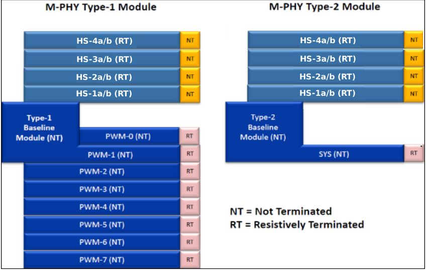
5.1.4 M-PHY Type
M-PHY can be of two types Type-I or Type-II. Both systems have similar functionality and features
for the High-Speed mode with support for HS-G1, HS-G2, HS-G3 and HS-G4. They however do differ
in the Low-Speed functionality. Figure below summarizes the available speeds between Type-I and
Type-II systems.
Figure 10: M-PHY Type1 and Type 2 Module
5.2 Overview of Arasan M-PHY for UFS
Arasan’s M-PHY utilizes the UFS requirements for M-PHY and consists of a power-efficient solution
for the architecture. The M-PHY consists of the analog transceivers, high speed PLL, data recovery
units as well as the state-machine control all in a single GDSII. The interface is compliant to M-PHY
pin configurations for seamless integration to the controller.
5.3 Arasan’s M-PHY for UFS Features
• Complaint to MIPI Alliance Standard for M-PHY specification Version 4.1
• Supports high speed data transfer G1A/B, G2A/B, G3A/B and G4A/B with data rates of up to
11660.8 Mb/s
• Supports M-PHY Type-I system
Copyright © 2021, Arasan Chip Systems Inc. 21Datasheet
• Support for reference clock frequencies of 19.2MHz/26MHz/38.4MHz/52MHz
• Reference clock shared between Host and device, as per UFS specification
• Supports low speed transfer G0-G7 with a bit rate of up to 576 Mb/s
• PWM signaling for Low speed [LS] data
• Supports error detection mechanism for sequence errors and contentions
• Data lanes support transfer of data in high-speed mode.
• Supports LS burst, HS burst, STALL, SLEEP, HIBERN8 states.
• Supports squelch detection
• Has clock divider unit to generate clock for parallel data reception and transmission from and to
the PIF.
• Activates and disconnects high speed terminators for reception and transmission.
• Supports standard PHY transceiver compliant to MIPI Specification
• Supports standard PIF interface compliant to MIPI Specification.
• On-chip clock generation configurable for either transmitter or a receiver
• Testability for Tx, Rx and PLL
Figure 11: ACS M-PHY for UFS Block Diagram
Copyright © 2021, Arasan Chip Systems Inc. 22Datasheet
5.4 M-PHY Pad Table
5.4.1 Functional Description of M-PHY Pads for Tx Lane
Table 3: Functional description of M-PHY Pads for Tx lane
Pin Direction Description
TXDP Output Positive polarity of low voltage differential clock signal
for transmitter
TXDN Output Negative polarity of low voltage differential clock signal
for transmitter
5.4.2 Functional Description of M-PHY Pads for Rx Lane
Table 4: Functional Description of M-PHY Pads for Rx Lane
Pin Direction Description
RXDP Input Positive polarity of low voltage differential data signal
for receiver
RXDN Input Negative polarity of low voltage differential data signal
for receiver
5.4.3 UFS Specific Pins
Table 5: UFS Specific Pins
Pin Direction Description
Refclk Input Reference clock (local for the Host)
5.4.4 Protocol Interface (PIF) Signals
Table 6: M-TX-CTRL Signals
Pin Direction Description
tx_cfgclk Input Transmit Control Interface Clock.
tx_reset Input Active-high asynchronous reset to reset M-TX.
Should be asserted for at least 100 ns.
tx_attrid[7:0] Input This signal indicates the configuration attributes for read
or write operations, or M-TX Capability attribute or
OMCS Status Attributes for read operation.
tx_attrrdval[7:0] Output Attribute Read data from M-TX.
tx_attrwrval[7:0] Input Attribute Write data to M-TX.
Input Attribute write enable to M-TX.
‘1‘ - Write operation.
Copyright © 2021, Arasan Chip Systems Inc. 23Datasheet
‘0’ - Read operation.
tx_cfgenbl Input Configuration Enable to M-TX.
This signal indicates an enable for attribute read or write
operation.
tx_inlncfg Input tx_inlncfg is used in conjunction with tx_attrwrn and
tx_cfgenbl to
direct a write operation to the M-TX's shadow memory
bank or to
the M-TX's effective configuration bank.
‘0’ - shadow memory bank.
‘1’ - effective configuration
Note: Unipro can only read from the effective
configuration bank.
tx_cfgupdt Input This signal indicates to transfer the contents of the
shadow memory to the effective configuration bank.
tx_cfgupdt Output This signal indicates whether M-TX is ready to accept
write data.
‘0’ - M-TX is ready to accept write data.
‘1’ - M-TX is not ready to accept write data.
tx_linereset Input This signal indicates M-TX to issue LINERESET.
tst_rtcontrol Input tst_rtcontrol carries real-time signals to control
implementation-specific signals, e.g. test features, inside
the M-TX. These signals are asynchronous to any clock
on the M-TXDATA or M-TX-CTRL interfaces.
Table 7: M-TX Data Transfer Signals
tx_savestate_status_n Output tx_savestate_status_n indicates the MTX is entering or
exiting a SAVE state. The Protocol Layer can use this
signal to understand when the M-TX is not transmitting
PREPARE, SYNC, HOB, PAYLOAD, TOB, BURST Extension
or LINE-CFG information. The M-TX sets
tx_savestate_status_n to “0” when it enters into a SAVE
state. The M-TX sets tx_savestate_status_n to “1” when
it exits a SAVE state.
tx_symbolclk Input M-TX DATA Symbol Clock
tx_phydirdy Input PHY Data Input Ready.
This signal indicates that M-TX is ready to accept new
data.
tx_symbol[79:0] Input tx_symbol is used for BURST data transfer to the M-TX.
The contents of this bus depend on the whether the
8b10b encoding function
in the M-TX is bypassed.
When the M-TX 8b10b encoding function is bypassed,
tx_symbol carries the raw data to send on the LINEs,
Copyright © 2021, Arasan Chip Systems Inc. 24Datasheet
parallelized according to the implemented width. The
LSb of tx_symbol shall correspond to the earliest
transmitted bit.
When the M-TX 8b10b encoding function is enabled, 32
LSbs of tx_symbol is used to carry the unencoded DATA
or control symbol. The M-TX shall ignore the unused
MSbs of tx_symbol.
tx_protdordy[7:0] Input PHY Data Output Ready
This signal indicates that data is available in the
corresponding tx_symbol.
tx_datanctrl[7:0] Input tx_datanctrl indicates the type of symbol on tx_symbol.
The bits of tx_datanctrl are mapped to the same as the
bits of
tx_protdordy.
‘0’ - data symbol.
‘1’ - control symbol.
tx_burst Input This active high signal indicates that burst is in progress.
tst_rtobserve Output tst_rtobserve makes internal M-TX realtime signals
observable, e.g. through DMA, by the Protocol Layer, or
external test equipment.
These signals are asynchronous to any clock on the M-
TX-DATA or
M-TX-CTRL interfaces.
tx_adapt_active Output TX_ADAPT_ACTIVE = 1 indicates to the Protocol that MTX is
in ADAPT sub-state. The signal is asserted after PREPARE.
The signal is de-asserted with the end of the ADAPT sequence.
tx_adapt_req Input The Protocol Layer shall set TX_ADAPT_REQ to “1” to initiate
an ADAPT sequence.
Once set to “1”, the M-TX shall send the PREPARE sequence
followed by the ADAPT sequence.
The Protocol shall de-assert TX_ADAPT_REQ with
TX_ADAPT_ACTIVE = 1 earliest, but latest with the end of the
ADAPT sequence when the MTX returns to STALL. The
Protocol Layer shall ensure RX_ADAPT_Control set to ADAPT
prior to assertion of this signal.
Table 8: M-RX CTRL Interface Signals
Signal Direction Description
rx_cfgclk Input Receive Control Interface Clock.
rx_reset Input Active-high asynchronous reset to reset M-RX.
Should be asserted for at least 100 ns.
rx_linereset Output This signal indicates the status of LINERESET.
‘1’ - LINERESET is detected.
‘0’ - LINERESET is in exit state
rx_attrid[7:0] Input This signal indicates the configuration attributes for read
or write operations, or M-RX Capability attribute or
OMCS Status Attributes for read operation.
rx_attrrdval[7:0 Output Attribute read value from M-RX.
Copyright © 2021, Arasan Chip Systems Inc. 25Datasheet
rx_attrwrval[7:0] Input Attribute write value to M-RX.
rx_attrwrn Input Attribute write enable to M-RX.
‘1‘ - Write operation.
‘0’ - Read operation.
rx_cfgenbl Input Configuration Enable to M-RX.
This signal indicates an enable for attribute read or write
operation.
rx_inlncfg Input rx_inlncfg is used in conjunction with rx_attrwrn and
rx_cfgenbl to direct a write operation to the M-RX's
shadow memory bank or to the M-RX's effective
configuration bank.
‘0’ - shadow memory bank.
‘1’ - effective configuration
Note: Unipro can only read from the effective
configuration bank.
rx_cfgupdt Input RX_CfgUpdt transfers the contents of the INLINE-CR
registry to the effective configuration bank during a
SAVE state.
rx_cfgrdyn Output This signal indicates whether M-RX is ready to accept
write data.
‘0’ - M-RX is ready to accept write data.
‘1’ - M-RX is not ready to accept write data.
rx_hibern8exit_t Output rx_hibern8exit_type-i indicates the M-RX is exiting
ype-i HIBERN8. The MRX sets RX_Hibern8Exit_Type-I to “1”
when it detects a DIF-Z to DIFN transition on the LINE.
The M-RX sets rx_hibern8exit_type-i to “0” when the
MRX is in either HIBERN8 or DISABLED state.
rx_lccrddet Output rx_lccrddet indicates that M-RX received an LCC-READ
sequence, which results in the update of corresponding
attributes in the M-RX.
tst_rtcontrol Input tst_rtcontrol carries real-time signals to control
implementation-specific signals, e.g. test features, inside
the M-RX. These signals are asynchronous to any clock
on the M-RXDATA or M-RX-CTRL interfaces.
Table 9: M-RX Data Interface Signals
Signal Direction Description
rx_symbolclk Input M-RX DATA Symbol Clock
rx_symbol[79:0] Input rx_symbol is used for BURST data transfer from the M-
RX.
When the 10b8b decoding function is bypassed,
rx_symbol carries the raw data as received on the LINEs,
parallelized according to the implemented width. The
LSb of rx_symbol shall correspond to the earliest
received bit.
Copyright © 2021, Arasan Chip Systems Inc. 26Datasheet
When the 10b8b decoding function is enabled; only the
32 LSbs of rx_symbol are used to carry the decoded
DATA or control symbol. The MRX shall set the
remaining MSbs to “0”.
rx_phydordy[7:0] Input PHY Data Output Ready
This signal indicates that data is available in the
corresponding rx_symbol.
rx_datanctrl[7:0] Input tx_datanctrl indicates the type of symbol on rx_symbol.
The bits of rx_datanctrl are mapped to the same as the
bits of rx_protdordy.
‘0’ - data symbol.
‘1’ - control symbol.
rx_burst Input This active high signal indicates that burst is in progress.
tst_rtobserve Output tst_rtobserve makes internal M-RX realtime signals
observable, e.g. through DMA, by the Protocol Layer, or
external test equipment. These signals are asynchronous
to any clock on the M-RXDATA or M-RX-CTRL interfaces.
5.5 Power Pads
Table 10: Power Pads
Pin Type Direction Description
VDDD POWER INOUT Power supply for Digital M-PHY
VSSD POWER INOUT
VDDPLL POWER INOUT Power supply for PLL
VSSPLL POWER INOUT
VDDB POWER INOUT Power supply for Bias Generation
VSSB POWER INOUT
VDD_IO POWER INOUT I/O power supply for internal LDO
VSS_IO POWER INOUT
5.5.1 Analog Configuration Bit (Trim Bits)
Table 11: Ports for trim_bits
Register Direction Description
trim_0[31:0] Input Trim bits for M-PHY
trim_1[31:0] Input Trim bits for M-PHY
trim_2[31:0] Input Trim bits for M-PHY
trim_3[31:0] Input Trim bits for M-PHY
Note: Since this is hard IP - pinout, it is subject to change depending on process node, feature etc.
5.6 Hard Macro Deliverables
Copyright © 2021, Arasan Chip Systems Inc. 27You can also read