Distilling nanoscale heterogeneity of amorphous silicon using tip-enhanced Raman spectroscopy (TERS) via multiresolution manifold learning - Nature
←
→
Page content transcription
If your browser does not render page correctly, please read the page content below

ARTICLE
                  https://doi.org/10.1038/s41467-020-20691-2                 OPEN

                  Distilling nanoscale heterogeneity of amorphous
                  silicon using tip-enhanced Raman spectroscopy
                  (TERS) via multiresolution manifold learning
                  Guang Yang 1 ✉, Xin Li1,4 ✉, Yongqiang Cheng1, Mingchao Wang2, Dong Ma                                            1,   Alexei P. Sokolov1,3,
                  Sergei V. Kalinin 1, Gabriel M. Veith 1 & Jagjit Nanda1 ✉
1234567890():,;

                  Accurately identifying the local structural heterogeneity of complex, disordered amorphous
                  materials such as amorphous silicon is crucial for accelerating technology development.
                  However, short-range atomic ordering quantification and nanoscale spatial resolution over a
                  large area on a-Si have remained major challenges and practically unexplored. We resolve
                  phonon vibrational modes of a-Si at a lateral resolution of
ARTICLE                                                                 NATURE COMMUNICATIONS | https://doi.org/10.1038/s41467-020-20691-2

S
       ilicon is central for a gamut of applications including large-        components)18,26. To date, there are a few studies in which TERS
       scale     integrated     electronic   circuits1,   photonics2,        was used for studying the structural heterogeneity of amorphous
       photovoltaics3,4, and energy storage units5–7. It is well             carbon27. The nanoscale structural heterogeneity and local
known that the essences of Si-based materials, including optical,            structure of a-Si have not been explored using TERS so far.
electrical8 properties, and nuclear spin9, are highly related to their          We herein illustrate a multiresolution analytical framework
atomic structures. Ever since Russell reported the first observation          based on graph-analytics and an unsupervised manifold learning
of the first-order inelastic Raman scattering in a Si single crys-            algorithm to facilitate identifying the nanoscale structure of a-Si
tal10, Raman spectroscopy has been intensively used to investigate           thin film. High-dimensional hyperspectral TERS mapping on the
the Si crystal structure11, phonon dispersion12, electronic states13,        a-Si thin film comprises thousands of TERS spectra. The multi-
local stress and strain14,15, and thermal properties16, which are            resolution manifold learning (MML) algorithm projects the TERS
integral to the performances of silicon-based devices. Despite its           mapping to a low dimensional (i.e. 2D) manifold space, thereby
versatility, the applications of micro-Raman spectroscopy to                 allowing for ease of straightforward data visualizations and
characterize the submicron-to-nanoscale chemistry and physics                structural categorization. Unlike traditional manifold learning
are severely restrained by the intrinsic diffraction limit of the            methods targeting solely on overlaying the prior-known labels
visible light (i.e. >200 nm) based on Abbe’s law17. Tip-enhanced             over the manifold points28, the MML proposed here does not
Raman spectroscopy (TERS) provides an apertureless means of                  require any prior bias regarding the material structure and
mapping Raman scattering at the nanometer scale (~10 nm) in-                 instrumental modality29,30. Benefiting from this nature, the
sample plane18,19. TERS is based on strong and local enhance-                underlying a-Si structural and physical properties, such as the
ment of the Raman signal by the surface plasmon resonance                    average Si–Si distortion angle and the strain-free energy can be
(SPR) on the metallic tip surface. Additionally, a non-resonant              quantified without a human-specified physical threshold at a
enhanced electromagnetic field (EM-field) occurs at the apex of                lateral spatial resolution of
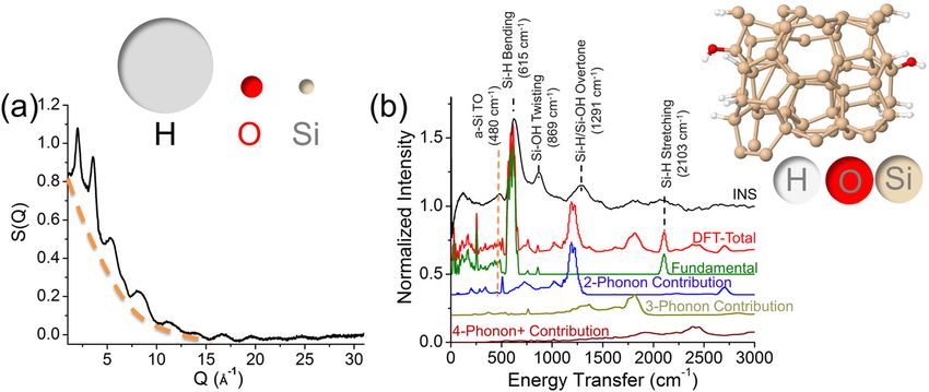
NATURE COMMUNICATIONS | https://doi.org/10.1038/s41467-020-20691-2                                                                    ARTICLE

Fig. 1 The integrated workflow comprising hyperspectral TERS imaging and the multi-resolution manifold learning (MML) algorithm. The low
dimensional physical parameters characterizing material structures such as local defects and atomic vibrations are translated into the high dimensional
Raman spectra via hyperspectral tip-enhanced Raman spectroscopy (TERS) imaging transfer functions. The intrinsic low dimensionality of the physics
suggests the structure of TERS measurements on the sample as a whole can be projected to a low dimensional latent manifold space via the
multiresolution manifold learning (MML). Exploration data analysis such as clustering can be efficiently conducted on the low-dimensional manifold space
to reveal salient features for evaluating material structure heterogeneity by human reasoning and updating domain knowledge in a loop.

graph construction and manifold layout can be found in the                      numerous other studies34–38, including the modes of the
“Method” section). Clustering can be subsequently performed on                  longitudinal-acoustic (LA, 312 cm−1), longitudinal-optical (LO,
the low-dimensional manifold to underpin the intrinsic structure                400 cm−1), and transverse-optical (TO, 473 cm−1), respectively34.
within the manifold that corresponds to the material structure                  The second-order phonon modes (denoted as 2LA and 2TO) of
heterogeneity. To better partition intrinsic manifold clusters                  either a-Si or c-Si tip are also observable (Fig. 2a). The intensity of
(facilitating clustering tasks), Li et al. recently proposed a Graph-           the second-order phonon modes is generally low, perhaps due to
Bootstrapping procedure29,30 that iteratively reconstructed the                 the off resonance of the laser frequency with the a-Si direct band
NN graph based on previous manifold positions and then                          gap39. Due to the low signal-to-noise ratio, such second-order
recalculated manifold coordinates based on the reconstructed NN                 phonon modes are difficult to be distinguished in standard
graph. The projected low dimensional manifold clusters represent                Raman spectroscopy (Fig. S3b) on a-Si, corroborating the
featured spectral property of the materials, thereby allowing for               essential role of TERS in this study. Note that the local laser
gaining insights of latent material structures via external valida-             power was set low (25 µW) to avoid laser-induced heating effect
tions such as first principle theories. This, in turn, benefits a                 on a-Si surface, which is known to be strong in TERS measure-
future experimental design with human-reasoning for gaining a                   ments40. It has been shown that above a threshold power density
deeper structure–property relationship of the materials (Fig. 1).               value, the laser-induced heating effect could alter the silicon
   The characteristic TERS spectra obtained from the a-Si surface               structures and ultimately affect the Raman measurements41. The
are shown in Fig. 2a. All spectra contain a sharp peak located at               local laser power density used here has shown to keep the a-Si
520 cm−1, ascribed to the first–order TO mode for the crystal                    surface intact in our previous report42. TERS mapping is able to
silicon derived from the TERS (Fig. S3). For c-Si, only the zone-               provide an overview of the intensity distribution of a given
center TO mode is detectable based on the excitation of the                     vibrational mode. The normalized intensity (at 520 cm−1 for TO
visible Raman laser to the lattices of the diamond structure, with              mode) of each vibrational peak is quantified by the color bar with
the Si–Si bond angle of 109.5o10,11,31. Notably, the coexistence of             the correspondence mapping representing the abundance of each
the a-Si and c-Si TO modes in Fig. 2a does not indicate that the a-             chemical moiety. Figure. 2b presents the relative intensity distribu-
Si is partially crystallized on the surface32. A further inspection on          tion of the a-Si TO mode (approximately centered at 473 cm−1). The
the a-Si surface using confocal micro-Raman spectroscopy with a                 TERS spectra taken from two spots (denoted as A and B) ~80 nm
much higher laser power did not reflect the existence of the c-Si                apart from each other exhibit different TO mode intensity (Fig. 2a).
TO band at 520 cm−1 (Fig. S3). Instead, a few broad Raman                       This clearly indicates that the a-Si surface phonon mode unveiled by
bands were featured in several frequency regions, indicating that               TERS expresses nanoscale heterogeneity. TERS mapping of the a-Si
the sputtered-silicon in this study is in the totally amorphous                 2LA mode is shown in Fig. 2c. Clearly, the feature of the intensity
state. The broadening of the several Raman bands results from                   distribution of 2LA mode differs from that of the TO mode shown in
the loss of the long-range translational symmetry and corre-                    Fig. 2b, demonstrating the highly heterogeneous feature of the pho-
sponding reciprocal lattice of the c-Si, which allows for detection             non modes on a-Si surface. It is also manifested the spectrum taken
of the entire phonon density of the states (DOS) across the whole               from Point C on the TERS map shows a larger 2LA mode intensity
first BZ zone reflected by the Raman spectra33. Though it is                      than those from Points A and B, but the TO band intensity is lower
inappropriate to correlate the traveling wave vectors to the                    than the latter two (Fig. 2a). The a-Si 2TO mode at 943 cm−1 has a
phonon feature in amorphous solids, we assign the a-Si TERS                     favorable distribution on the upper side of the scanned region
bands to phonon frequencies for ease of comparison with                         (Fig. 2d), different from the distribution of the above-mentioned

NATURE COMMUNICATIONS | (2021)12:578 | https://doi.org/10.1038/s41467-020-20691-2 | www.nature.com/naturecommunications                              3
ARTICLE                                                                   NATURE COMMUNICATIONS | https://doi.org/10.1038/s41467-020-20691-2

Fig. 2 TERS spectra from selected locations and TERS mappings based on a single peak. a The tip-enhanced Raman spectroscopy (TERS) spectra
collected from various locations on the amorphous silicon a-Si surface labeled by “A” to “D” in (b–d). TERS mapping of an individual peak intensity centered
at (b) 473 cm-1 (a-Si transvers optical or TO mode), (c) 642 cm-1 (2nd-order longitudinal acoustic or 2LA mode), and (d) 943 cm−1 (2TO mode). A hybrid
TERS mapping combining the peak intensity distribution in (b–d) is shown in Fig. S2. The color bar scales the single peak intensity for each TERS mapping.

phonon modes. The TERS mapping generated based on a single-                    categorized into seven clusters (Fig. 3a) in the 2D manifold space.
mode intensity clearly demonstrates that (i) TERS is capable of                Here we denote these clusters as “parent clusters” to differentiate
depicting the a-Si phonon mode in nanoscale, and (ii) the abundance            from the “child clusters” derived at finer resolution grids in
of different a-Si phonon modes is highly heterogeneous and varies              manifold space. The mean TERS spectrum of each cluster is
across the scanned area. The TERS enhancement of the 3rd and 4th               shown in Fig. 3b. An immediate observation on Fig. 3b is that the
order phonon modes is unobvious (See Fig. S5).                                 TO band at ~470 cm−1 intensity varies among clusters. The
   The mapping analysis based on the single variant method (i.e.               intensity of the second-order phonon peaks also varies, although
intensity of a single TERS band) is insufficient to lead to a                   not much obvious as the TO mode. To quantify the analysis on
comprehensive understanding of the surface structure of the a-                 the TERS bands below 600 cm−1, we implemented peak decon-
Si18. Analysis based on an individual TERS band by nature fails to             volution of the overlapped phonon vibrational modes of a-Si,
capture the overall spectral pattern of TERS mapping. To retain                including LA, LO, TO modes and c-Si TO mode. A TERS peak
the global features embedded in the full set of TERS spectra, we               deconvolution example is given in Fig. 3c based on the spectrum
then performed manifold learning and clustering of TERS spec-                  of cluster 0. It is noteworthy that further improving the dispersion
tral dataset (see details in method section). Note that the TERS               by using grating with more groves per mm didn’t assist in better
mapping was implemented on a 1 × 1 µm2 area with a 20 nm step                  resolving the phonon modes of the a-Si (Fig. S9). The atomistic
size, it yields 2500 TERS spectra in total, with a lateral spectral            level local structure of a-Si random network is characterized by
resolution approximately

NATURE COMMUNICATIONS | https://doi.org/10.1038/s41467-020-20691-2                                                                       ARTICLE

Fig. 3 The parent manifold layout, mean TERS spectra and transverse optical mode peak position via Graph-Bootstrapping algorithm. a The parent
manifold layout via the Graph-Bootstrapping method (see details in “Method” section) colored by the cluster labels. b The mean tip-enhanced Raman
spectroscopy (TERS) spectrum for each cluster (spectrum normalized against the c-Si transverse optical or TO mode at 520 cm−1). c Peak deconvolution
of the silicon TO modes, longitudinal optical (LO) mode and longitudinal acoustic (LA) mode. d The TO-band center arranged in declining order. The error
bar stands for the Gaussian fitting deviation of the peak center. Δθ is defined as the deviation of the Si–Si bond angle in the a-Si random network from that
of the single-crystal Si (109.5°).

sensitive to
ARTICLE                                                                  NATURE COMMUNICATIONS | https://doi.org/10.1038/s41467-020-20691-2

Fig. 4 Viability evaluation of TERS spectral clustering by the multiresolution manifold learning algorithm and the similarity loading. a Average
tip-enhanced Raman spectroscopy (TERS) spectrum of each cluster and its nearest neighbor in experimental data. b Similarity loading of each cluster.
The color bar represents the reciprocal of Euclidean distance between the mean TERS spectrum and the as-taken TERS spectrum of each pixel within
a given cluster.

percentage
NATURE COMMUNICATIONS | https://doi.org/10.1038/s41467-020-20691-2                                                                           ARTICLE

Fig. 5 The child clusters at the finer resolution grid. a An overview of child manifold clusters at the finer resolution grid, stemmed from Parent Cluster 2
and (b) the corresponding mean tip-enhanced Raman spectroscopy (TERS) spectra of the child clusters. The peak centered at 2435 cm-1 of Child Cluster 8
represents unique structural defects different from other child clusters. c Similarity loading of Child Cluster 8 that shows a bright blob around the black
singular patches in similarity loading of Parent Cluster 2 in Fig. 4. d Overview of child clusters stemmed from Parent Cluster 0 and (e) the corresponding
mean Raman spectra of the child clusters. f The similarity loading of Child Cluster 1 that shows a bright blob around the black singular patches in Parent
Cluster 0 similarity loading in Fig. 4. The color bar represents the reciprocal of Euclidean distance between the mean TERS spectrum and the as-taken TERS
spectrum of each the pixel within a given cluster.

Fig. 6 The neutron scattering plot and inelastic neutron scattering spectrum of a-Si. a Neutron scattering plot of the structure factor, S versus the
scattering vector, Q collected from amorphous silicon a-Si under the same sputtering condition to deposit the a-Si thin film. The dashed curve guides the
eye as an indication of the background from incoherent scattering. Inset schematically illustrates the relative size of the incoherent scattering cross-section
(XS) of proton (80.260), the coherent XS of oxygen (4.232), and the coherent XS of silicon (2.163). b Comparison between the experimental inelastic
neutron scattering spectrum of the amorphous silicon a-Si sample and that calculated using DFT based on the atomic conformations shown in the inset
image. The calculated total spectrum combines the fundamental vibrational modes and higher order excitations up to 10 orders.

broad background shown in Fig. 6a due to incoherent scattering                   2189 cm−159,. Given that the surface selection rule complied by
from H. The reactions between the air water and dangling Si bond                 TERS differs from those for IR and Raman18, it is difficult to
results in silane- and siloxane- type moieties on a-Si (see Sup-                 precisely predict the active TERS vibrational modes for SiHx
porting Information).                                                            compounds in this frequency region.
   The simplest protonated Si compound is Si–H. The reported                        Inelastic neutron scattering spectroscopy (INS) allows for
Raman scattering center for monohydrate (Si-H) ranges between                    measuring the vibrational modes in the absence of the selection
2030 cm−158,. and 2090 cm−159,. Binding more protons to Si                       rules for hydrogen atom60, thereby exhibiting a comprehensive
leads to blueshift of the Si–H stretching mode, with the maximum                 picture of all possible vibrational modes on the a-Si sample used
frequency found for hydrogenated sputtered Si–H4 compound at                     here. Figure 6b shows an INS spectrum of the a-Si sample. To

NATURE COMMUNICATIONS | (2021)12:578 | https://doi.org/10.1038/s41467-020-20691-2 | www.nature.com/naturecommunications                                      7
ARTICLE                                                                 NATURE COMMUNICATIONS | https://doi.org/10.1038/s41467-020-20691-2

unambiguously assign the vibrational modes, we further per-                  nanoscale structure, such as defects of semiconductor devices in
formed density functional theory (DFT) calculation on a surface              both fundamental research and industrial applications.
hydrogenated a-Si, assuming a “water splitting” mechanism (see                  While the current study solely focuses on a-Si thin film, the
supporting information) to form the Si–H and Si–OH functional                combination of ultra-sensitive surface spectroscopy, TERS and
groups on the a-Si surface (Fig. 6b, inset). The existence of the –H         the efficient multiresolution manifold learning algorithm should
and –OH functional groups in the a-Si sample is validated by the             boost scientific discoveries in a broad scope of disciplines, such as
excellent agreement between the experimental INS spectrum and                solid-state electrolytes, metal–organic framework (MOF), and
that calculated by DFT in Fig. 6b. The most distinguished proof of           low-dimension materials, revealing the unknown unknowns to
the Si–H bond presence is the Si–H bending mode centered at                  material and domain scientists.
615 cm−1. The presence of the Si–OH groups is evidenced by the
Si–OH twisting bands centered at 869 cm−1 from INS spec-                     Methods
trum61. Intriguingly, both experimental and DFT calculated INS               a-Si thin film deposition. The a-Si thin film was RF magnetron sputtered onto a
spectra show a broad band at around 2430 cm−1, assigned to the               copper foil using a Si target (99.99%, Kurt J. Lesker) in an in-house sputtering
4-phonon overtone of the Si–H bending mode. In fact, the Si–H                device. Base pressure was below 5 × 10⁻⁸ Torr and the target to substrate distance
                                                                             was 7 cm. The thickness of the a-Si was 50 nm as measured by a quartz-crystal
stretching vibrational mode (frequency as ν) is closely related to           microbalance (QCM). This type of a-Si thin film was then used for TERS mea-
the electronegativity of the near-neighbor surroundings, with a              surement. To increase the amount of material for neutron experiments, 20 µm a-Si
simplified induction model formulated as62                                    films were deposited on the copper substrates. Immediately after the deposition, the
                                                                             a-Si samples were transferred to an Ar-filled glovebox (O2 < 0.1 ppm, H2O < 0.1
                          ν ¼ ν o þ bΣXA                              ð2Þ    ppm) in less than one minute.

where νo and b are empirically derived constants and XA is
                                                                             TERS setup and measurements. A physical vapor deposition (PVD) method was
defined as the stability-ratio (SRX) electronegativity63. The values          used to fabricate TERS probes from commercial AFM tips (Bruker, OTESPA-R3,
of νo and b were found to be 1741 and 34.7 for molecular com-                resonance frequency = 300 kHz, spring constant = 26 N/m, tip apex diameter = 7
pounds, respectively62. The sum is over three neighbors, assum-              nm)18. Briefly, three sequential depositions of chromium (Cr) (2 nm adhesion
ing tetracoodination among the neighboring atoms with the                    layer), silver (Ag, plasmonic layer, ~40 nm), and aluminum (Al, protection layer,
                                                                             1.5 nm) were performed. Al converts to a dense alumina that provides good
central Si. Different atomic species have various values of SRX,             mechanical and chemical protection without influencing significantly on tip optical
namely XSi = 2.62, XH = 3.55, and XO = 5.2161.                               properties. TERS tip fabrication details can be found in Reference65. A shiny
   In this context, the Si-H stretching mode can further blueshift           lithium foil was put aside with the sample. There was no observable color change of
to above 2250 cm−161,64. Based on Eq. (2), the highest possible              the lithium foil over the course of TERS measurement, indicating a decent inert gas
frequency for Si-H stretching mode calculated is 2283 cm−1 for               quality inside the glove box. All TERS measurements were performed on an atomic
                                                                             force microscope (AFM, AIST-NT SMART PROBE) in connection with a Raman
O3–Si–H type compound. However, this value is still 152 cm−1                 spectrometer (HORIBA Co., Xplore) in an argon-filled glove box. For TERS
lower than the X-mode shown in the TERS spectrum in Parent                   measurements, the 532 nm laser wavelength was chosen with a local power density
Cluster 2, Child Cluster 8 (Fig. 5b). Given that the a-Si thin film is        of 25 µW. The grating number was 600 grooves/mm, and the objective was 100×
highly disordered on the surface intrinsically, we reason that there         (N.A. = 0.7). The tapping mode was chosen with oscillation amplitude of 20 nm
                                                                             and a ~2 nm minimum distance from the sample surface for AFM. The mapped
possibly exists overly coordinated surface Si atoms of low abun-             area was set at 1 × 1 µm2 with a step size of 20 nm. The accumulation time was 0.5
dance. We herein define Xe as the excess SRX electronegativity                s for each spectral acquisition. Each frame of TERS map represents the intensity
contributed from the excess coordination (>4) to the Si. For the             (after background correction) of the corresponding vibrational mode that arises
case of X-mode of the TERS band, Xe was calculated at 4.4, close             from a-Si. The total illumination time for taking a TERS mapping was approxi-
                                                                             mately 20.8 min
to the reported value for the suboxide silicon as an effective media
for a-Si61. In this case, the central Si may form the orthosilicate-
type compound with the oxygen in surrounding suboxide silicon.               FDTD simulation. Three-dimensional (3D) finite-difference time-domain (FDTD)
                                                                             simulations (Lumerical Solutions, Inc.) were used to study the electromagnetic
Thus, the larger blueshift of the X-mode TERS band than gen-                 (EM-field) distribution between the tip apex and the a-Si sample. The FDTD model
erally reported values originates from overcoordination of the               is shown in Fig. S1a. Briefly, a silver tip of a 42 nm diameter at the apex was coated
Si–H with the surrounding suboxide (i.e. Ox–Si–Hy, x + y > 4).               with 1.5 nm Al2O3 layer (see Fig. S1b). The tip was set 2 nm from the Si surface.
Since in the same frequency region, as a bulk sensitive spectro-             The tip axis had an angle of 10° with the vector of the sample plane. A plane wave
                                                                             of electric field, E, polarized along the blue double-arrow in Fig. S1a propagates
scopy technology, INS shows only a broad shoulder (Fig. 6b), the             along the vector. The laser propagation direction is at 55o relative to the perpen-
abundance of the overcoordination Si compound should thus be                 dicular direction of the Si substrate. The wavelength of the plane wave was set at
critically low. It is therefore worth emphasizing that the existence         532 nm. The spatial mesh size was set at 0.1 nm. The perfectly matched layer
of the trace amount (
NATURE COMMUNICATIONS | https://doi.org/10.1038/s41467-020-20691-2 ARTICLE
graph; (2) For each neighbor node j of node i, calculate Euclidean distances Density functional theory (DFT) calculations. DFT modeling was performed
between node i and each neighbor node l of node j, distði; lÞ ¼ kxi xj k; (3) Push l using the Vienna ab initio Simulation Package (VASP)84. The calculation used
with dist(i,l) into Hi; (4) Pop if Hi has more than k nodes. For each node i and each Projector Augmented Wave (PAW) method 85,86, to describe the effects of core
neighbor node j of i, an edge E(i,j) is added to the graph. The weight of symmetric electrons, and Perdew–Burke–Ernzerhof (PBE)87 implementation of the General-
edge E(i,j) is defined in a similar way of t-sne method69: ized Gradient Approximation (GGA) for the exchange-correlation functional.
Energy cutoff was 600 eV for the plane-wave basis of the valence electrons. The
pjji þ pijj expðjjxi xj jj2 =2δ 2i Þ starting structure of a-Si slab with both surfaces terminated by –H and -OH was
wij ¼ ; pjji ¼ P 2 ð3Þ generated by MD simulations as discussed above78. The thickness of the slab is
ði;k2EÞ expðjjxi xk jj =2δ i Þ
2n 2
about 1.5 nm, and the total thickness of the simulation box is 3.5 nm (i.e., 2 nm
To calculate a low-dimensional manifold layout of the graph where each node i vacuum). The surface area is about 1.05 nm × 1.05 nm. The simulation box
of graph is represented by a point yi in 2D space, a likelihood function is contains 64 Si atoms, and is under 3D periodic boundary condition. The electronic
constructed to preserve pair-wise similarities of the nodes in the 2D space66, structure was calculated on a 3 × 3 × 1 Monkhorst–Pack mesh. The total energy
Y Y tolerance for electronic energy minimization was 10−5 eV, and the maximum
Lðy1 ; y2 ; :::; yn Þ ¼ ½f ðjjyi yj jjÞwij ½1 f ðjjyi yj jjÞε
ð4Þ interatomic force after relaxation was below 0.01 eV/Å. The vibrational eigen-
ði;jÞ2E ði;jÞ2E frequencies and modes were then calculated by the finite displacement method.
The OClimax software88 was used to convert the DFT-calculated phonon results to
where f is a probability function set as f ðxÞ ¼ and ε is a unified weight.
1
1þx2 the simulated INS spectra.
Intuitively, first part of the above equation will keep similar nodes close in 2D space
meanwhile second part will tell apart dissimilar nodes in 2D space. The likelihood
function can be efficiently maximized with respect to ðy1 ; y2 ; :::; yn Þ via negative Data availability
sampling70 and alias table sampling71 of unfolded weighted edges72, followed by The data that support the findings of this study are available from the corresponding
asynchronous stochastic gradient descent73. During implementations, we set all authors upon reasonable request.
hyperparameters default as in LargeVis66 without any signal pre-processing.
Clustering on manifold is performed by hierarchical density estimates method
(HDBSCAN)74–76, which relies on the mutual reachability distance: Code availability
The codes that support the findings of this study are available from the corresponding
Dmreach;K ða; bÞ ¼ maxfcorek ðaÞ; corek ðbÞ; dða; bÞg ð5Þ authors upon reasonable request.
where d(a,b) is the original metric distance (Euclidean distance in this paper)
between points a and b, corek(x) is the core-distance of a point x to cover its k Received: 25 June 2020; Accepted: 14 December 2020;
nearest neighbors. A minimum spanning tree is firstly built and then condensed
upon the hyper-parameter of minimum cluster size, mc. The stability of each
cluster Ci is defined as:
X
SðCi Þ ¼ a2C
ðλmax;Ci ;a λmin;Ci ;a Þ ð6Þ References
i
1. Chen, R. et al. Nanophotonic integrated circuits from nanoresonators grown
where λ is the reciprocal of core-distance, λmax;Ci ;a is the λ value at which point a on silicon. Nat. Commun. 5, 1–10 (2014).
falls out of cluster Ci and λmin;Ci ;a is the minimum λ value at which point a is 2. Vivien, L. & Pavesi, L. Handbook of Silicon Photonics (Taylor & Francis, 2016).
present in Ci. Optimal flat clusters are extracted via walking up the tree to 3. Ndiaye, A. et al. Degradations of silicon photovoltaic modules: a literature
maximize the total stability score over chosen clusters: considering all leaf nodes as review. Sol. Energy 96, 140–151 (2013).
initial clusters, if the cluster’ stability is greater than the sum of its child, the cluster 4. Kim, J. et al. 10.5% efficient polymer and amorphous silicon hybrid tandem
is selected to be in the current set of optimal flat clustering and all its child are photovoltaic cell. Nat. Commun. 6, 1–6 (2015).
removed from the set. Otherwise, the cluster’s stability is set to be the sum of its 5. Hou, T. et al. The influence of FEC on the solvation structure and reduction
child stabilities. The main tuning parameter is the minimum cluster size, mc. We reaction of LiPF6/EC electrolytes and its implication for solid electrolyte
leave all the other tuning parameters of HDBSCAN as default. For the parent interphase formation. Nano Energy 64, 103881 (2019).
manifold clusters in Fig. 3, we follow a similar procedure in ref. 21 to choose mc. 6. Wu, H. et al. Stable cycling of double-walled silicon nanotube battery anodes
We first consider all integer mc values in a wide range of [10,150]. We then fit the through solid–electrolyte interphase control. Nat. Nanotechnol. 7, 310
trend of total number of estimated clusters against every mc value by the (2012).
exponential decay function. We choose the mc in the tail region where the total 7. Ryu, J. et al. Infinitesimal sulfur fusion yields quasi-metallic bulk silicon for
number of clusters tends to be stable. For child manifold clusters at the finer stable and fast energy storage. Nat. Commun. 10, 1–9 (2019).
resolution grid as shown in Fig. 5, we set the mc a small value around 0.5% of the 8. Hasan, M., Huq, M. F. & Mahmood, Z. H. A review on electronic and optical
total number of TERS measurements. properties of silicon nanowire and its different growth techniques.
SpringerPlus 2, 151 (2013).
Neutron scattering. All neutron scattering measurements were performed at the 9. Kane, B. E. A silicon-based nuclear spin quantum computer. nature 393, 133
Spallation Neutron Source at Oak Ridge National Laboratory (ORNL). Prior to (1998).
each measurement, the a-Si film was peeled off from the copper substrate in the Ar- 10. Russell, J. P. Raman scattering in silicon. Appl. Phys. Lett. 6, 223–224 (1965).
filled glovebox (O2 < 0.1 ppm, H2O < 0.1 ppm) and sealed in a vanadium can (Ø = 11. Parker, J. Jr., Feldman, D. & Ashkin, M. Raman scattering by silicon and
6 mm). The total amount of a-Si was 1.368 g and the height was 3.9 cm. An empty germanium. Phys. Rev. 155, 712 (1967).
vanadium can of the same type was sealed in Ar-glovebox and used as a blank 12. Richter, H., Wang, Z. & Ley, L. The one phonon Raman spectrum in
reference. microcrystalline silicon. Solid State Commun. 39, 625–629 (1981).
13. Yue, G., Lorentzen, J., Lin, J., Han, D. & Wang, Q. Photoluminescence and
a. Neutron total scattering structure function. The structure function data were Raman studies in thin-film materials: transition from amorphous to
collected at Nanoscale-Ordered Materials Diffractometer (NOMAD) beam- microcrystalline silicon. Appl. Phys. Lett. 75, 492–494 (1999).
line per a procedure published by Neuefeind et al.77. The data collection 14. De Wolf, I. Micro-Raman spectroscopy to study local mechanical stress in
time was 150 min The structure factor, S(Q) was obtained from a Q range silicon integrated circuits. Semiconductor Sci. Technol. 11, 139 (1996).
between 0.5 and 31 Å−1. 15. Zeng, Z. et al. In situ measurement of lithiation-induced stress in silicon
b. Inelastic neutron scattering (INS). INS spectra were obtained at the VISION nanoparticles using micro-Raman spectroscopy. Nano Energy 22, 105–110
beamline on the same a-Si measured by neutron PDF to assure consistency.
(2016).
The sample was measured in vanadium sample holder at 5 K for about 10 h.
16. Perichon, S., Lysenko, V., Remaki, B., Barbier, D. & Champagnon, B.
The empty sample holder was also measured, and the background spectrum
Measurement of porous silicon thermal conductivity by micro-Raman
was removed to obtain the spectrum from the sample.
scattering. J. Appl. Phys. 86, 4700–4702 (1999).
17. Wang, X., Huang, S.-C., Hu, S., Yan, S. & Ren, B. Fundamental understanding
Molecular Dynamics (MD) simulations. The models of a-Si were established by and applications of plasmon-enhanced Raman spectroscopy. Nat. Rev. Phys. 2,
conducting molecular dynamics simulations in LAMMPS78. Following a melting- 253–271 (2020).
and-quench procedure79, the initial network a-Si was firstly annealed to 2400 K in 18. Nanda, J. et al. Unraveling the nanoscale chemical heterogeneity of solid
the NVT ensemble, and then quenched to room temperature (300 K) at a quench electrolyte interphase using tip-enhanced Raman spectroscopy. Joule 3,
rate of 1012 Ks−1. The a-Si models were finally fully relaxed at 300 K in the NPT 2001–2019 (2019).
ensemble. The SW-VBM interatomic potential80 was used to describe Si–Si 19. Yano, T.-a. et al. Tip-enhanced nano-Raman analytical imaging of locally
interaction. The average coordination number of constructed a-Si models is ~3.99 induced strain distribution in carbon nanotubes. Nat. Commun. 4, 1–7 (2013).
and quite close to the experimental value (~3.8–3.9)81–83, validating the high 20. Gersten, J. I. The effect of surface roughness on surface enhanced Raman
quality of these a-Si models. scattering. J. Chem. Phys. 72, 5779–5780 (1980).
NATURE COMMUNICATIONS | (2021)12:578 | https://doi.org/10.1038/s41467-020-20691-2 | www.nature.com/naturecommunications 9ARTICLE NATURE COMMUNICATIONS | https://doi.org/10.1038/s41467-020-20691-2
21. Asghari‐Khiavi, M. et al. Exploring the origin of tip‐enhanced Raman 55. Beeman, D., Tsu, R. & Thorpe, M. Structural information from the Raman
scattering; preparation of efficient TERS probes with high yield. J. Raman spectrum of amorphous silicon. Phys. Rev. B 32, 874 (1985).
Spectrosc. 43, 173–180 (2012). 56. Squires G. L. Introduction to the Theory of Thermal Neutron Scattering
22. Sonntag, M. D. et al. Recent advances in tip-enhanced Raman spectroscopy. J. (Cambridge University Press, 2012).
Phys. Chem. Lett. 5, 3125–3130 (2014). 57. Sears, V. F. Neutron scattering lengths and cross sections. Neutron News 3,
23. Sun, W. & Shen, Z. A practical nanoscopic Raman imaging technique realized 26–37 (1992).
by near-field enhancement. Mater. Phys. Mech. 4, 17–21 (2001). 58. Volodin, V. & Koshelev, D. Quantitative analysis of hydrogen in amorphous
24. Lee, N. et al. High contrast scanning nano‐Raman spectroscopy of silicon. J. silicon using Raman scattering spectroscopy. J. Raman Spectrosc. 44,
Raman Spectrosc. 38, 789–796 (2007). 1760–1764 (2013).
25. Brockhouse, B. Lattice vibrations in silicon and germanium. Phys. Rev. Lett. 2, 59. Brodsky, M., Cardona, M. & Cuomo, J. Infrared and Raman spectra of the
256 (1959). silicon-hydrogen bonds in amorphous silicon prepared by glow discharge and
26. Sendek, A. D. et al. Holistic computational structure screening of more than sputtering. Phys. Rev. B 16, 3556 (1977).
12000 candidates for solid lithium-ion conductor materials. Energy Environ. 60. Harrelson, T. F. et al. Identifying atomic scale structure in undoped/doped
Sci. 10, 306–320 (2017). semicrystalline p3ht using inelastic neutron scattering. Macromolecules 50,
27. Kharintsev, S. S., Saparina, S. V., Fishman, A. I., Stolov, A. A. & Li, J. Spectrally 2424–2435 (2017).
resolving coherent TERS spectroscopy of electrically biased carbon-coated 61. Tsu, D., Lucovsky, G. & Davidson, B. Effects of the nearest neighbors and the
fibers. J. Phys. Chem. C 124, 14752–14758 (2020). alloy matrix on SiH stretching vibrations in the amorphous SiO r: H (0< r< 2)
28. Zhong, M. et al. Accelerated discovery of CO2 electrocatalysts using active alloy system. Phys. Rev. B 40, 1795 (1989).
machine learning. Nature 581, 178–183 (2020). 62. Lucovsky, G. Chemical effects on the frequencies of Si-H vibrations in
29. Li, X. et al. High-veracity functional imaging in scanning probe microscopy amorphous solids. Solid State Commun. 29, 571–576 (1979).
via Graph-Bootstrapping. Nat. Commun. 9, 2428 (2018). 63. Sanderson, R. T. Chemical periodicity (Reinhold Pub. Corp., 1960).
30. Li, X. et al. Manifold learning of four-dimensional scanning transmission 64. Borghesi, A., Guizzetti, G., Sassella, A., Bisi, O. & Pavesi, L. Induction-model
electron microscopy. npj Comput. Mater. 5, 5 (2019). analysis of Si H stretching mode in porous silicon. Solid state Commun. 89,
31. Morell, G. et al. Raman study of the network disorder in sputtered and glow 615–618 (1994).
discharge a‐Si: H films. J. Appl. Phys. 78, 5120–5125 (1995). 65. Barrios, C. A., Malkovskiy, A. V., Kisliuk, A. M., Sokolov, A. P. & Foster, M.
32. Tsu, R., Gonzalez-Hernandez, J. & Pollak, F. H. Determination of the energy D. Highly stable, protected plasmonic nanostructures for tip enhanced Raman
barrier for structural relaxation in amorphous Si and Ge by Raman scattering. spectroscopy. J. Phys. Chem. C. 113, 8158–8161 (2009).
Solid state Commun. 54, 447–450 (1985). 66. Tang J., Liu J., Zhang M., Mei Q. Visualizing large-scale and high-dimensional
33. Zallen, R. Physics of Amorphous Solids (John Wiley & Sons, 2008). data. In Proce. 25th International Conference on World Wide Web
34. Morimoto, A., Ooroza, S., Kumeda, M. & Shimizu, T. Raman studies on local (International World Wide Web Conferences Steering Committee, 2016).
structural disorder in silicon-based amorphous semiconductor films. Solid 67. Dasgupta, S. & Freund, Y. Random projection trees and low dimensional
state Commun. 47, 773–777 (1983). manifolds. In STOC (Citeseer, 2008).
35. Voutsas, A., Hatalis, M., Boyce, J. & Chiang, A. Raman spectroscopy of 68. Dong, W., Moses, C. & Li, K. Efficient k-nearest neighbor graph construction
amorphous and microcrystalline silicon films deposited by low‐pressure for generic similarity measures. In Proc. 20th International Conference on
chemical vapor deposition. J. Appl. Phys. 78, 6999–7006 (1995). World Wide Web (ACM, 2011).
36. Tsu, R., Gonzalez-Hernandez, J., Doehler, J. & Ovshinsky, S. Order parameters 69. Maaten, L. V. D. & Hinton, G. Visualizing data using t-SNE. J. Mach. Learn.
in a-Si systems. Solid state Commun. 46, 79–82 (1983). Res. 9, 2579–2605 (2008).
37. Sinke, W., Roorda, S. & Saris, F. Variable strain energy in amorphous silicon. 70. Mikolov, T., Sutskever, I., Chen, K., Corrado, G. S. & Dean, J. Distributed
J. Mater. Res. 3, 1201–1207 (1988). representations of words and phrases and their compositionality. In Advances
38. Vink, R., Barkema, G. & Van Der Weg, W. Raman spectra and structure of in Neural Information Processing Systems) (ACM, 2013).
amorphous Si. Phys. Rev. B 63, 115210 (2001). 71. Li, A. Q., Ahmed, A., Ravi, S. & Smola, A. J. Reducing the sampling
39. Renucci, J., Tyte, R. & Cardona, M. Resonant Raman scattering in silicon. complexity of topic models. In Proc. 20th ACM SIGKDD International
Phys. Rev. B 11, 3885 (1975). Conference on Knowledge Discovery and Data mining) (ACM, 2014).
40. Malkovskiy, A. et al. Tip‐induced heating in apertureless near‐field optics. J. 72. Tang, J. et al. Line: Large-scale information network embedding. In Proc. 24th
Raman Spectrosc. 40, 1349–1354 (2009). International Conference on World Wide Web (International World Wide
41. Han, L., Zeman, M. & Smets, A. H. Raman study of laser-induced heating Web Conferences Steering Committee, 2015).
effects in free-standing silicon nanocrystals. Nanoscale 7, 8389–8397 (2015). 73. Recht, B., Re, C., Wright, S. & Niu, F. Hogwild: A lock-free approach to
42. Nanda, J. et al. Unraveling the nanoscale heterogeneity of solid electrolyte parallelizing stochastic gradient descent. In Advances in Neural Information
interphase using tip-enhanced Raman spectroscopy. Joule 3, 2001–2019 (2019). Processing Systems (NIPS, 2011).
43. Treacy, M. & Borisenko, K. The local structure of amorphous silicon. Science 74. Campello, R. J., Moulavi, D. & Sander, J. Density-based clustering based on
335, 950–953 (2012). hierarchical density estimates. In Pacific-Asia Conference on Knowledge
44. Brodsky, M. & Cardona, M. Local order as determined by electronic and Discovery and Data Mining) (Springer, 2013).
vibrational spectroscopy: amorphous semiconductors. J. Non-Crystalline 75. McInnes, L., Healy, J. & Astels, S. hdbscan: Hierarchical density based
Solids 31, 81–108 (1978). clustering. J. Open Source Softw. 2, 205 (2017).
45. Alben, R., Weaire, D., Smith, J. Jr. & Brodsky, M. Vibrational properties of 76. McInnes L, Healy J. Accelerated hierarchical density based clustering[C]//
amorphous Si and Ge. Phys. Rev. B 11, 2271 (1975). 2017 IEEE International Conference on Data Mining Workshops (ICDMW).
46. Keating, P. Effect of invariance requirements on the elastic strain energy of IEEE. 33–42 https://doi.org/10.1109/ICDMW.2017.12 (2017).
crystals with application to the diamond structure. Phys. Rev. 145, 637 (1966). 77. Neuefeind, J., Feygenson, M., Carruth, J., Hoffmann, R. & Chipley, K. K. The
47. Tsu, R. in (David Adler and Brian B. Schwartz eds) Disordered Semiconductors nanoscale ordered materials diffractometer NOMAD at the spallation neutron
(Springer, 1987). source SNS. Nucl. Instrum. Methods Phys. Res. B: Beam Interact. Mater. At.
48. Saito, T., Karasawa, T. & Ohdomari, I. Distortion energy distributions in the 287, 68–75 (2012).
random network model of amorphous silicon. J. Non-Crystalline Solids 50, 78. Plimpton, S. Fast parallel algorithms for short-range molecular dynamics. J.
271–276 (1982). Comput. Phys. 117, 1–19 (1995).
49. Steinhardt, P., Alben, R. & Weaire, D. Relaxed continuous random network 79. Sitinamaluwa, H., Nerkar, J., Wang, M., Zhang, S. & Yan, C. Deformation and
models:(I). Struct. Charact. J. Non-Crystalline Solids 15, 199–214 (1974). failure mechanisms of electrochemically lithiated silicon thin films. RSC Adv.
50. Vignoli, S. et al. Over-coordination and order in hydrogenated nanostructured 7, 13487–13497 (2017).
silicon thin films: their influence on strain and electronic properties. J. Phys.: 80. Vink, R., Barkema, G., Van der Weg, W. & Mousseau, N. Fitting the
Condens. Matter 17, 1279 (2005). Stillinger–Weber potential to amorphous silicon. J. Non-crystalline Solids 282,
51. Deringer, V. L. et al. Realistic atomistic structure of amorphous silicon from 248–255 (2001).
machine-learning-driven molecular dynamics. J. Phys. Chem. Lett. 9, 81. Kugler, S. et al. Neutron-diffraction study of the structure of evaporated pure
2879–2885 (2018). amorphous silicon. Phys. Rev. B 40, 8030 (1989).
52. Barkema, G. & Mousseau, N. Event-based relaxation of continuous disordered 82. Fortner, J. & Lannin, J. Radial distribution functions of amorphous silicon.
systems. Phys. Rev. Lett. 77, 4358 (1996). Phys. Rev. B 39, 5527 (1989).
53. Mousseau, N. & Barkema, G. Traveling through potential energy landscapes of 83. Roorda, S. et al. Structural relaxation and defect annihilation in pure
disordered materials: The activation-relaxation technique. Phys. Rev. E 57, amorphous silicon. Phys. Rev. B 44, 3702 (1991).
2419 (1998). 84. Kresse, G. & Furthmüller, J. Efficient iterative schemes for ab initio total-
54. Marinov, M. & Zotov, N. Model investigation of the Raman spectra of energy calculations using a plane-wave basis set. Phys. Rev. B 54, 11169 (1996).
amorphous silicon. Phys. Rev. B 55, 2938 (1997). 85. Blöchl, P. E. Projector augmented-wave method. Phys. Rev. B 50, 17953 (1994).
10 NATURE COMMUNICATIONS | (2021)12:578 | https://doi.org/10.1038/s41467-020-20691-2 | www.nature.com/naturecommunicationsNATURE COMMUNICATIONS | https://doi.org/10.1038/s41467-020-20691-2 ARTICLE
86. Kresse, G. & Joubert, D. From ultrasoft pseudopotentials to the projector experiments. Y.C. did INS data analysis and DFT calculations. M.W. performed MD
augmented-wave method. Phys. Rev. B 59, 1758 (1999). simulations. D.M. performed the neutron PDF experiments and data analysis. A.P.S.
87. Perdew, J. P., Burke, K. & Ernzerhof, M. Generalized gradient approximation assisted in TERS design and analyzed the TERS data. S.V.K. provided supervision on
made simple. Phys. Rev. Lett. 77, 3865 (1996). MML design, coding and assisted in proof demonstration. G.V. designed and prepared a-
88. Cheng, Y., Daemen, L., Kolesnikov, A. & Ramirez-Cuesta, A. Simulation of Si thin film samples. J.N. administrated the project and provided the funding source. All
inelastic neutron scattering spectra using OCLIMAX. J. Chem. Theory authors contributed to writing, revising and reviewing the manuscript.
Comput. 15, 1974–1982 (2019).
Competing interests
The authors declare no competing interests.
Acknowledgements
This work is supported by the U.S. Department of Energy’s Vehicle Technologies Office
under the Silicon Electrolyte Interface Stabilization (SEISta) Consortium directed by Additional information
Brian Cunningham and managed by Anthony Burrell. Part of this work was supported Supplementary information is available for this paper at https://doi.org/10.1038/s41467-
by the Center for Nanophase Materials Sciences, a U.S. Department of Energy, Office of 020-20691-2.
Science User Facility at Oak Ridge National Laboratory (S.V.K), Division of Materials
Science and Engineering, Biomolecular Materials Program, and Energy Frontier Research Correspondence and requests for materials should be addressed to G.Y., X.L. or J.N.
Center CSSAS located at University of Washington (X.L.). A portion of this research used
resources at the Spallation Neutron Source, a DOE Office of Science User Facility Peer review information Nature Communications thanks Sergey Kharintsev, Zee Hwan
operated by the Oak Ridge National Laboratory. Computing resources for DFT simu- Kim and the other, anonymous, reviewer(s) for their contribution to the peer review of
lations were made available through the VirtuES and the ICE-MAN projects, funded by this work. Peer reviewer reports are available.
Laboratory Directed Research and Development program and Compute and Data
Environment for Science (CADES) at ORNL. APS acknowledges support from DOE BES Reprints and permission information is available at http://www.nature.com/reprints
Materials Science and Engineering Division for TERS analysis and description. We thank
Dr. Dmitry N. Voylov for useful discussion on the TERS experimental setup. We are Publisher’s note Springer Nature remains neutral with regard to jurisdictional claims in
grateful for fruitful discussions on RF sputtering with Drs. Nancy J. Dudney, Andrew published maps and institutional affiliations.
Kercher, and Robert L. Sacci. We thank Drs. Andrew Westover, Jue Liu and Katharine L.
Page discussion for NOMAD setup. We thank Michelle S. Everett for strong technical
support for NOMAD. This manuscript has been authored by UT-Battelle, LLC under
Open Access This article is licensed under a Creative Commons
Contract No. DE-AC05-00OR22725 with the U.S. Department of Energy. The United
Attribution 4.0 International License, which permits use, sharing,
States Government retains and the publisher, by accepting the article for publication,
adaptation, distribution and reproduction in any medium or format, as long as you give
acknowledges that the United States Government retains a non-exclusive, paid-up,
appropriate credit to the original author(s) and the source, provide a link to the Creative
irrevocable, world-wide license to publish or reproduce the published form of this
Commons license, and indicate if changes were made. The images or other third party
manuscript, or allow others to do so, for United States Government purposes. The
Department of Energy will provide public access to these results of federally sponsored material in this article are included in the article’s Creative Commons license, unless
research in accordance with the DOE Public Access Plan (http://energy.gov/downloads/ indicated otherwise in a credit line to the material. If material is not included in the
doe-public-access-plan). article’s Creative Commons license and your intended use is not permitted by statutory
regulation or exceeds the permitted use, you will need to obtain permission directly from
the copyright holder. To view a copy of this license, visit http://creativecommons.org/
Author contributions licenses/by/4.0/.
G.Y. and J.N. conceived and designed the TERS experiments. G.Y. and X.L. conceived the
multiresolution manifold learning (MML) for TERS mapping. X.L. developed the codes
for MML. G.Y. and X.L. wrote the initial draft. Y.C. and G.Y. performed the INS © The Author(s) 2021
NATURE COMMUNICATIONS | (2021)12:578 | https://doi.org/10.1038/s41467-020-20691-2 | www.nature.com/naturecommunications 11You can also read