Effects of PCB Technological Features on Channel Operating Margin (COM) - 14TH CENTRAL PA SYMPOSIUM ON SIGNAL INTEGRITY : vTools Events (ieee.org) ...
←
→
Page content transcription
If your browser does not render page correctly, please read the page content below
Effects of PCB Technological Features on Channel
 Operating Margin (COM)

14TH CENTRAL PA SYMPOSIUM ON SIGNAL INTEGRITY : vTools Events (ieee.org) 16 Apr 2021
Longfei Bai. Simulia-CST, Dassault Systèmes, Dr. Tracey Vincent, Heavyside Corp.
Abstract
 The coupling (weak vs. strong) in edge-coupled differential transmission lines on a printed
 circuit board (PCB) affects frequency behavior of mixed-mode S-parameters. Slightly
 imbalanced stripline differential pairs are considered with various technological features
 modeled: rectangular vs. trapezoid shape of a signal trace cross-section; copper foil
 roughness; and presence of an epoxy-resin " pocket " (EP) between the stripline traces
 (dielectric properties of the EP are different from the homogenized parameters of the
 ambient dielectric where these traces are embedded. The quality of the differential mode
 (DM), which determines SI, is associated with the frequency dispersion and loss on the
 line. The common mode (CM) is inevitable on differential pairs. The study is carried out
 using full-wave simulation and corroborated with measurement. After the differential pairs
 are examined, the model is used for the calculation of COM. Channel Operating Margin
 (COM) is an efficient method to evaluate high speed interconnects. Effects of PCB
 technologies on COM are studied with a 1000GBASE-KP4 link. The pulse responses of COM
 are validated by comparing to circuit simulations.

 April 22, 2021 2
Outline
 This is a two-step presentation. The first step (see below). The second
 step is a calculation of the COM with the same features.
 The first step overview:
 ❖Motivation
 ❖What do you mean by “Technological Features”
 ❖Discuss the features of interest
 ❖Simulated results (focus on mode conversion)
 ❖Measured results

 April 22, 2021 3

Motivation

 • Differential signaling plays an important part in high-speed digital design due to their high
 immunity, low X-talk, and potentially reduced EMI problems.
 • Currently, high-speed serial link interfaces, e.g., USB, Ethernet, InfiniBand, PCI Express, Serial
 Attached SCSI, operate in the differential signal transmission mode, and have from a few to tens
 gigabit-per-second data rates.
 • Transmission line/net features have an impact on the mode conversion of the signals.

 April 22, 2021 4
Modes Edge Coupled Stripline

 Differential / Odd Mode Common/ Even Mode

 April 22, 2021 5
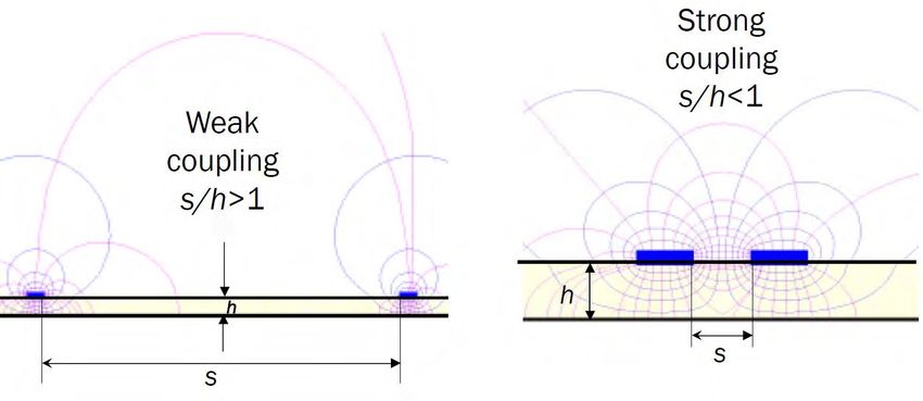
Topological features and material factors on Signal Integrity
of differential pair
 Stripline edge coupled differential pair were compared for
 • Weak and strong coupled case
 • Trace shape: Rectangular edge; trapezoid edges of 60 and 45 degrees
 • With/without copper foil roughness
 • With/without epoxy-resin “pocket”

 Gap depends on weak or strong coupling
 Surface roughness
 Trace Edge shape
 (rectangle shown)
 Epoxy Pocket

 M. Koledintseva, T. Vincent, “Comparison of Mixed-mode S-parameters in Weak and Strong coupled Differential Pairs”. Conference:
 2016 IEEE International Symposium on Electromagnetic Compatibility - EMC 2016
Strong vs Weak coupling metric
 Weak coupled: Zdiff = 97.44, Zcom = 26.11 K= - 0.034

 Strong coupled: Zdiff = 83.22, Zcom = 25.48, K= - 0.096

 Zdiff = 2Zodd = 2Zse(1-K)

 Zcom = Zeven/2=(Zse/2)(1+K)

 Zdiff + 4*Zcom = 97.44+4*26.11 = 201 = 4*Zse. Zse=50.47 Example: Weak coupled

 Zdiff + 4*Zcom = 83.22+4*25.48 = 185.14 = 3*Zse. Zse=46.285

 April 22, 2021 7
Weak and strong coupling

 April 22, 2021 8

Trace edge shapes Cross section views from models showing trapezoid shape.

 60 degree edge. Weak coupled, epoxy 90 degree edge. Strong coupled. No other
 pocket. features included in this model.

 45 degree edge. Weak coupled. Epoxy
 pocket (transparent).
 April 22, 2021 9
Copper foil Roughness

 Surface roughness modelled as dielectric layer on traces
 Drum, or “oxide” side

 Matte, or “foil” side

 This inhomogeneous
 ERD (surface roughness). Strong coupled, interface layer
 rectangle edge, with epoxy pocket. “copper-dielectric” is
 substituted by ERD

 April 22, 2021 10
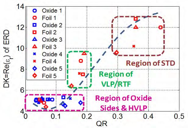
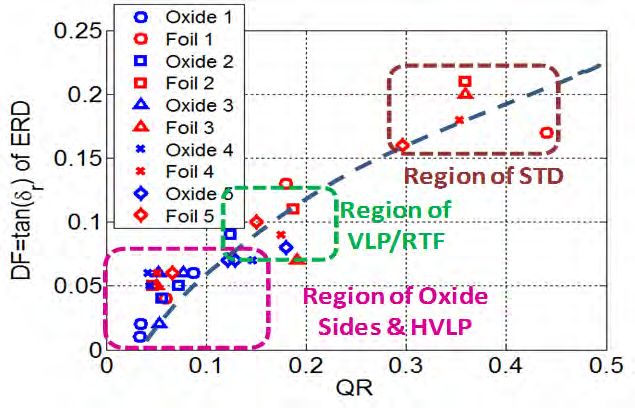
Quantification of Copper Foil Roughness Profiles 1st look at the surface measurement – and a look at a more sophisticated approach. “Oxide”, or drum side Ar- average peak-to-valley roughness amplitude Ar r t r – average quasi-period of roughness “Foil”, or matte side Tr QR – roughness quantification factor, QR~ Ar/r t – copper foil thickness (at flat levels) Tr – height of copper foil roughness layer in a model y x 5 0 -5 100 80 50 60 Ar, µm 40 0 x, µm 20 0 -50 11
Effective Roughness Dielectric (ERD) Parameters Extraction “smooth” conductor Roughness Dielectric contribution/ contribution contribution skin effect T = a + b + c + d 2 + e + f 2 a + b = K1 c + e = K2 d + f = K3 ▪Curve fitting co-efficients are generated K1 ~ √ω , K2 ~ ω, and K3 ~ ω² ▪K1(0), K2(0), and K3(0) corresponds with smooth conductor, allow separation of surface roughness loss and Reference: Koul, Koledintseva, Hinaga, dielectric loss. K co-efficients relate to Ar Drewniak “Differential Extrapolation ▪Dielectric material (smooth) 3D object with extracted Method for Separating Dielectric and “roughness” parameters can be included in simulation to Rough Conductor Losses in Printed simulate roughness impact Circuit Boards” IEEE Trans, 2012. 12
Effective Roughness Dielectric (ERD) Parameters Extraction Measurements of S- parameters w1 Tr oxide w2 Tr foil Extraction of true DK and DF of PCB dielectric (DERM) Optimization procedure uses numerical modeling in 2D-FEM the loop for fitting S- Model Criteria for Satisfied parameters until acceptable agreement of Extracted ERD measured and rough= rough-j rough measured and rough= rough-j rough modeled results agree modeled S21 within some criteria. (both IL & phase) Correction Validation by full- wave simulation Not satisfied M.Y. Koledintseva, T. Vincent, A. Ciccomancini Scogna, and S. Hinaga, “Method of effective roughness dielectric in a PCB: measurement and full-wave simulation verification”, IEEE Trans. Electromag. Compat., vol. 57, no. 4, Aug. 2015, pp. 807-814
Surface Roughness Model used - DERM

 Sets 1,2,3 – 13mil traces
 Thicknesses of the corresponding roughness dielectric layers
 Sets 4, 5 – 7 mil traces
 in the numerical model are taken as Tr=2×Ar

 April 22, 2021 14
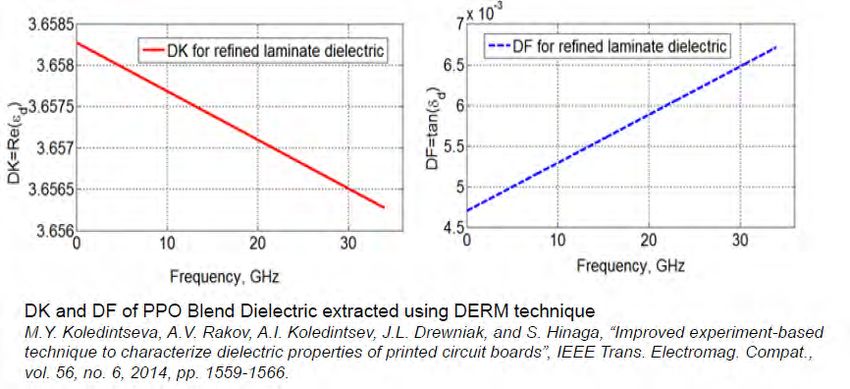
Simulation – layer of Dielectric Laminate fiberglass filled Copper foil composite dielectric Cross section view - Not to conductors scale for presentation purposes only Foil side ‘roughness Tr foil dielectric’ • Laminate dielectric parameters are extracted from DERM2 (for both and ). • Heights of ERD Tr foil are taken 2Ar foil, respectively. • Line length for this model = 15,410 mils 15
Conductor Roughness in Single-Ended Lines
 Conductor roughness affects both phase and loss constants in PCB transmission lines and results in eye diagram closure,
 especially at bit rates > 10 GBps.

 3 Gbps 28 Gbps

 HVLP

 VLP
 VLP

 STD

 April 22, 2021 16
Epoxy Pocket
 Epoxy pocket between traces

 Epoxy pocket between traces. Strong Epoxy pocket shown in magenta with 60
 coupled, rectangle edge, with ERD degree edge. Weak coupled,
 (surface roughness included)

 April 22, 2021 17
PCB material (matrix) properties

 April 22, 2021 18
Simulation
 • Using time domain solver due to broad band of results 0-40 GHz and low number of ports.
 • Multiple lengths, average ~100mm. For COM length the models were changed to 1meter.
 • Mesh count, for 100 mm length average mesh count was 2million, for 1m long pair the
 mesh count average was 25 million hexahedrals.

 Cross section mesh view
Differential-mode propagation with ERD (surface Roughness), different edge
gradients
 Stripline, with ERD Stripline, with ERD
 -10 0
 rect. trace: strong coupling
 rect. trace: weak coupling
 -15
 450 trap. trace: strong coupling
 -20 450 trap. trace: weak coupling
 -5 600 trap. trace: strong coupling
 -25
 600 trap. trace: weak coupling

 , dB
 , dB

 dd21
 -30
 dd11

 rect. trace: strong coupling

 S
 S

 -35 rect. trace: weak coupling -10
 0
 45 trap. trace: strong coupling
 -40
 450 trap. trace: weak coupling
 -45 600 trap. trace: strong coupling
 600 trap. trace: weak coupling
 -50 -15
 0 5 10 15 20 25 30 35 40 0 5 10 15 20 25 30 35 40
 Frequency, GHz Frequency, GHz

• Weak coupling provides less IL for DM than strong coupling.
• Rectangular traces provide less IL for DM than the trapezoidal traces, especially in the weak-coupled lines. IL in the 45-
 degree case is higher than in 60-degree case for the weak coupling.
• IL in the 45-degree and 60-degree strong-coupled cases almost coincide, and they are higher than in the rectangular case.
Differential-mode propagation

 Stripline Stripline
 -5 0
 rect. trace: no ERD, weak coupling
 -10 rect. trace: with ERD, weak coupling
 -15

 -20 -5
 X: 39.8

 , dB
 , dB

 Y: -7.046
 -25

 dd21
 dd11

 -30

 S
 S

 -35 -10
 X: 39.84
 Y: -12.09
 -40

 -45 rect. trace: no ERD, weak coupling
 rect. trace: with ERD, weak coupling
 -50 -15
 0 5 10 15 20 25 30 35 40 0 5 10 15 20 25 30 35 40
 Frequency, GHz Frequency, GHz

There is difference of about 5.0 dB at 40 GHz for the given lengths of the traces in the IL for the DM propagation.
Differential-mode propagation

 Stripline, rectangular traces Stripline, rectangular traces
 -5 0

 -10

 -15

 -20 -5
 X: 39.96
 , dB

 , dB
 Y: -7.087
 -25
 dd11

 dd21
 -30
 S

 S
 X: 39.96
 -35 -10 Y: -10.75

 -40
 no ERD, with epoxy pocket, weak coupling no ERD, with epoxy pocket, weak coupling
 with ERD, with epoxy pocket, weak coupling X: 39.96
 -45 with ERD, with epoxy pocket, weak coupling Y: -12.11
 with ERD, no epoxy pocket, weak coupling with ERD, no epoxy pocket, weak coupling
 -50 -15
 0 5 10 15 20 25 30 35 40 0 5 10 15 20 25 30 35 40
 Frequency, GHz Frequency, GHz

Comparing two ERD cases – with epoxy resin pockets and without, there is a difference of about 1.4 dB at 40
GHz for the given lengths of the traces in the IL for the DM propagation due to the epoxy pocket. This difference
is less than for the strong-coupled case.
Differential-mode propagation

 Stripline, 600 trapezoid traces Stripline, 600 trapezoid traces
 -5 0
 no ERD, with epoxy pocket, weak coupling
 -10 with ERD, with epoxy pocket, weak coupling
 with ERD, no epoxy pocket, weak coupling
 -15

 -20 -5
 , dB

 , dB
 -25 X: 39.96
 dd11

 Y: -8.048

 dd21
 -30
 S

 S
 -35 -10 X: 39.96
 Y: -11.82
 -40
 no ERD, with epoxy pocket, weak coupling
 -45 with ERD, with epoxy pocket, weak coupling
 with ERD, no epoxy pocket, weak coupling X: 39.96
 -50 -15
 Y: -13.34
 0 5 10 15 20 25 30 35 40 0 5 10 15 20 25 30 35 40
 Frequency, GHz Frequency, GHz

Comparing two ERD cases – with epoxy resin pockets and without, there is a difference of about 1.5 dB at 40
GHz for the given lengths of the traces in the IL for the DM propagation due to the epoxy pocket.
Differential-mode propagation

 Stripline, 600 trapezoid traces Stripline, 600 trapezoid traces
 -5 0

 -10

 -15

 -20 -5
 , dB

 , dB
 -25
 dd11

 dd21
 X: 39.96
 Y: -8.894
 -30

 S
 S

 -35 -10 X: 39.96
 Y: -9.633

 -40
 no ERD, with epoxy pocket, strong coupling no ERD, with epoxy pocket, strong coupling
 X: 39.96
 -45 with ERD, with epoxy pocket, strong coupling with ERD, with epoxy pocket, strong coupling Y: -14.63
 with ERD, no epoxy pocket, strong coupling with ERD, no epoxy pocket, strong coupling
 -50 -15
 0 5 10 15 20 25 30 35 40 0 5 10 15 20 25 30 35 40
 Frequency, GHz Frequency, GHz

• IL for DM in the case with ERD, but no epoxy pocket is significantly less than in the cases with the epoxy pocket at
 lower frequencies (
Mode conversion (Sdc=Scd)

 Stripline, with ERD
 Stripline, with ERD -20
 -40
 -25
 -50
 -30
 -60
 -35

 , dB
 Sdc11, dB

 -70
 -40

 dc21
 rect. trace: strong coupling rect. trace: strong coupling
 -80

 S
 rect. trace: weak coupling -45 rect. trace: weak coupling

 -90 450 trap. trace: strong coupling 450 trap. trace: strong coupling
 -50
 450 trap. trace: weak coupling 450 trap. trace: weak coupling
 -100 600 trap. trace: strong coupling -55 600 trap. trace: strong coupling
 600 trap. trace: weak coupling 600 trap. trace: weak coupling
 -110 -60
 0 10 20 30 40 0 5 10 15 20 25 30 35 40
 Frequency, GHz Frequency, GHz
• In the strong-coupled cases, the mode conversion is reduced as compared to the weak-coupled cases.
• The weak-coupled case with 45-degree trapeziodal traces has the highest mode conversion over the entire frequency range.
• For rectangular traces, there is no significant difference in the mode conversion between the strong and weak coupling.
• The 60-degree traces provide the least mode conversion, especially in the strong-coupled cases.
Simulation Results
 Mode conversion (Sdc=Scd)
 Stripline, no ERD Stripline, no ERD
 -40 -20

 -25
 -50
 -30
 -60
 -35

 , dB
 Sdc11, dB

 -70
 rect. trace: strong coupling
 -40

 dc21
 rect. trace: weak coupling
 rect. trace: strong coupling
 -80 0

 S
 45 trap. trace: strong coupling -45 rect. trace: weak coupling
 0
 45 trap. trace: weak coupling 450 trap. trace: strong coupling
 -90 -50
 600 trap. trace: strong coupling 450 trap. trace: weak coupling
 600 trap. trace: weak coupling -55 600 trap. trace: strong coupling
 -100
 600 trap. trace: weak coupling
 -110 -60
 0 10 20 30 40 0 5 10 15 20 25 30 35 40
 Frequency, GHz Frequency, GHz

• In the strong-coupled cases, the mode conversion is reduced as compared to the weak-coupled cases. The same is seen with ERD. But
 without ERD, in the case with rectangular traces, strong coupling results in the higher mode conversion.
• The weak-coupled case with 60-degree trapeziodal traces has the lowest mode conversion over the entire frequency range.
• There is no much difference in the mode conversion levels for 45- and 60-degree cases in both strong-coupled and weak-coupled
 structures.
• ERD looks more important for mode conversion enhancement in 45-degree weak-coupled case.
Simulation Results
 Mode conversion (Sdc=Scd)
 Stripline
 Stripline
 -35
 -20
 rect. trace: no ERD, strong coupling
 rect. trace: with ERD, strong coupling
 -40 -25

 -30
 -45
 , dB

 , dB
 dc11

 -35

 dc21
 -50
 S

 S
 -40

 -55
 -45
 rect. trace: no ERD, strong coupling
 rect. trace: with ERD, strong coupling
 -60 -50
 0 5 10 15 20 25 30 35 40 0 5 10 15 20 25 30 35 40
 Frequency, GHz Frequency, GHz
 • There is a noticeable mode conversion enhancement due to ERD at the lower frequencies below 27 GHz, then ERD
 damps the mode conversion.
Simulation Results
 (Sdc=Scd)
 Mode conversion
 Stripline
 Stripline -20
 -35
 rect. trace: no ERD, weak coupling
 rect. trace: with ERD, weak coupling -25
 -40

 -30

 , dB
 -45
 , dB

 -35

 dc21
 dc11

 -50
 S

 S
 -40

 -55
 -45
 rect. trace: no ERD, weak coupling
 rect. trace: with ERD, weak coupling
 -60
 0 5 10 15 20 25 30 35 40 -50
 Frequency, GHz 0 5 10 15 20 25 30 35 40
 Frequency, GHz
• There is a noticeable mode conversion enhancement due to ERD at the lower frequencies below 23 GHz, then ERD
 results in damping.
• But the observed low-frequency enhancement in the weak-coupled case is less than for the strong-coupled case.
Simulation Results
 Mode conversion (Sdc=Scd)
 Stripline
 Stripline
 -20
 -35
 450 trap. trace: no ERD, strong coupling
 450 trap. trace: no ERD, strong coupling
 -40 450 trap. trace: with ERD, strong coupling
 450 trap. trace: with ERD, strong coupling -25
 -45

 -50 -30

 , dB
 , dB

 -55
 -35

 dc21
 dc11

 -60

 S
 S

 -65 -40

 -70
 -45
 -75

 -80 -50
 0 5 10 15 20 25 30 35 40 0 5 10 15 20 25 30 35 40
 Frequency, GHz Frequency, GHz

 • There is damping of mode conversion by ERD over the frequency range starting from 8 GHz in the
 strong-coupled and 45-degree trapezoidal case.
Simulation Results
 Mode conversion (Sdc=Scd)
 Stripline Stripline
 -35 -20
 450 trap. trace: no ERD, weak coupling 450 trap. trace: no ERD, weak coupling
 -40
 450 trap. trace: with ERD, weak coupling -25 450 trap. trace: with ERD, weak coupling
 -45

 -50 -30

 , dB
 , dB

 -55
 -35

 dc21
 dc11

 -60

 S
 S

 -65 -40

 -70
 -45
 -75
 -50
 -80 0 5 10 15 20 25 30 35 40
 0 5 10 15 20 25 30 35 40
 Frequency, GHz
 Frequency, GHz

 • There is significant damping of mode conversion by ERD over the entire frequency range in the weak-coupled and
 45-degree trapezoidal case.
Mode conversion (Sdc=Scd)

 Stripline, 600 trapezoid traces Stripline, 600 trapezoid traces
 -35 -20
 no ERD, with epoxy pocket, strong coupling no ERD, with epoxy pocket, strong coupling
 -40 with ERD, with epoxy pocket, strong coupling with ERD, with epoxy pocket, strong coupling
 with ERD, no epoxy pocket, strong coupling -25 with ERD, no epoxy pocket, strong coupling
 -45

 -50 -30
 , dB

 , dB
 -55
 dc11

 -35

 dc21
 -60
 S

 S
 -65 -40

 -70
 -45
 -75

 -80 -50
 0 5 10 15 20 25 30 35 40 0 5 10 15 20 25 30 35 40
 Frequency, GHz Frequency, GHz

• In the ERD cases, with 60-degree traces and strong coupling, epoxy pockets damp mode conversion.
• ERD also damps mode conversion over the entire frequency range.
• However, at the lower frequencies (
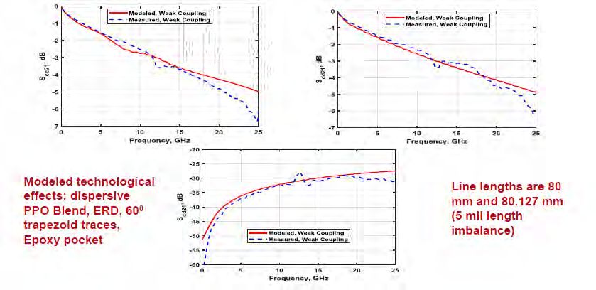
Measured vs simulation comparison; stripline, strong
coupled

 April 22, 2021 32
Measured vs simulation comparison; stripline, weak
coupled

 April 22, 2021 33
Conclusion
 ❖ For differential mode insertion loss the results were as expected: ERD (surface
 roughness) increases IL. Weak coupling has less impact when compared to strong
 coupling. Sharper angles has larger impact than rectangular edge overall.
 ❖ For SI, weak coupling is preferable – as expected.
 ❖ However, mode conversion is, in general, larger in the weak-coupled than strong-
 coupled cases especially if the traces are trapezoid and other factors are considered.
 ❖ It seems Copper foil roughness and the epoxy-resin pocket, between the traces,
 enhances mode conversion.
 ❖ The mode conversion is most critical when there is weak coupling, 45-degree trapezoid
 traces, and significant roughness (especially at lower frequencies). Strong coupling
 creates mode damping.
Effects of PCB Technological
 Features on Channel
© Dassault Systèmes | 4/22/2021 | ref.: 3DS_Document_2020

 Operating Margin (COM)
Abstract
 The coupling (weak vs. strong) in edge-coupled differential transmission lines on a printed circuit board
 (PCB) affects frequency behavior of mixed-mode S-parameters. Slightly imbalanced stripline differential
 pairs are considered with various technological features modeled: rectangular vs. trapezoid shape of a
 signal trace cross-section; copper foil roughness; and presence of an epoxy-resin " pocket " (EP) between
© Dassault Systèmes | 4/22/2021 | ref.: 3DS_Document_2020

 the stripline traces (dielectric properties of the EP are different from the homogenized parameters of the
 ambient dielectric where these traces are embedded. The quality of the differential mode (DM), which
 determines SI, is associated with the frequency dispersion and loss on the line. The common mode (CM) is
 inevitable on differential pairs. The study is carried out using full-wave simulation and corroborated with
 measurement. After the differential pairs are examined the model is used for the calculation of COM.

 Channel Operating Margin (COM) is an efficient method to evaluate high speed interconnects. Effects of
 PCB technologies on COM are studied with a 1000GBASE-KP4 link. The pulse responses of COM are
 validated by comparing to circuit simulations.

 36
Part 2: Channel Operating Margin [1][2]
© Dassault Systèmes | 4/22/2021 | ref.: 3DS_Document_2020

 ❑ COM Introduction
 ❑ COM Results for the Reference Model
 ❑ Comparison of COM Values for Models with
 different PCB technological features
 ❑ Summary

 37
COM: Channel Operating Margin

 100GBASE-KP4 [1]

 ➢ 100G: Data rate is about 100 Gbps Signaling rate 13.59375 GBd
 ➢ BASE: Baseband channel Receiver 3 dB bandwidth 0.75 ×
© Dassault Systèmes | 4/22/2021 | ref.: 3DS_Document_2020

 ➢ K: Backplane
 Number of signal levels 4
 ➢ P: PAM4
 ➢ 4: 4 differential pairs

 …
 …

 …
 Target detector error ratio 0 3 × 10⁻⁴
 ➢ About 1 meter long backplane channel in the
 Ethernet network, including daughter COM parameters
 boards, connectors and mother boards.

 ➢ COM parameters are provided in IEEE Std.
 802.3bj-2014

 38
FFE: Feed Forward Equalizer CTF: Continuous Time Filter
 Rd: Termination resistance DFE: Decision Feedback Equalizer

 Motivation PKG: Package
 SDD: Differential S-Parameter
 PDF: Probability Density Function
 COM: Channel Operating Margin
 NE/FEXT: Near/Far End Crosstalk SER: Symbol Error Rate PDF/COM/SER

 Tx Rx
 FFE Rd PKG PKG Rd CTF DFE
 Filter XT* Filter
© Dassault Systèmes | 4/22/2021 | ref.: 3DS_Document_2020

 SDD
 Tming Jitter ,
 Tx *The XT can be either
 FFE Rd PKG Sampling time
 Filter FEXT or NEXT.

 Die Package Board Package Die
 ➢ S-parameter is not enough to estimate the performance of the entire system.
 ➢ All the blocks are analytically formulated with the given COM parameters and together
 with SDD, PDF/COM/SER can be calculated to give qualitative evaluation on the passive
 channel.
 39
SDD: Differential S-parameter FFE: Feed Forward Equalizer
 PR: Pulse Response CTF: Continuous Time Filter

 COM Workflow FOM: Figure of Merit
 PDF: Probability Density Function
 PDF: Probability Density Function

 COM: Channel Operating Margin

 1. SDD 2. PR 3. FOM 4. PDF 5. COM
© Dassault Systèmes | 4/22/2021 | ref.: 3DS_Document_2020

 1. Differential S-parameter obtained from 3D simulation;
 2. Pulse response can be derived from SDD, including linear package parasitics
 and linear filters (e.g. FFE, CTF and receiver noise filter);
 3. Sweep parameters of FFE and CTF to find the best equalization setup based
 on FOM;
 4. Calculate PDF with the optimized FFE and CTF settings at step 3;
 5. Calculate COM value from the PDF obtained at step 4.

 40
SDD: Differential S-parameter
 NE/FEXT: Near/Far End Crosstalk

 1. SDD
 Transmitter 1 THRU SDD21 2 Victim
 Path k = 0
© Dassault Systèmes | 4/22/2021 | ref.: 3DS_Document_2020

 FEXT SDD24 NEXT SDD24
 Aggressor 3 4 Aggressor
 Path k = 1 Path k = 2

 ➢ Only differential mode is considered.
 ➢ SDD is normalized to100 Ohm.
 ➢ Linear sampled with equidistance of 0.01 GHz in the range [0, 56 GHz].
 ( )
 ➢ Frequency domain response ( ) for each path can be derived from S-parameter.

 41
PR: Pulse Response SDD: Differential S-Parameter
 FFE: Feed Forward Equalizer CTF: Continuous Time Filter

 2. PR Rd: Termination Resistance
 PKG: Package
 DFE: Decision Feedback Equalizer
 iFFT: inverse Fast Fourier Transform

 Tx Rx
 FFE Rd PKG SDD PKG Rd CTF DFE
 Filter Filter
© Dassault Systèmes | 4/22/2021 | ref.: 3DS_Document_2020

 ( )
 Parameterized taps: −1 , (1) ( ) Parameterized DC gain: g

 Linear part: ( ) ( ) v
 ℎ 0
 ( ) ℎ 0 ( ) : PR of THRU channel
 DFE taps : the first zero crossing before the peak
 iFFT : Unit Interval / Bit Time
 Pulse Response: ℎ( ) ( ) t

 Zero Crossing

 ➢ PRs can be calculated for the linear part and DFE taps can be read from ℎ 0 ( ).
 ➢ FFE and CTF are parameterized and PRs need to be calculated for every combination of these
 parameters.
 42
FOM: Figure of Merit PR: Pulse Response
 ISI: Inter Symbol Interference FFE: Feed Forward Equalizer

 3. FOM XT: Crosstalk
 TX: Transmitter
 CTF: Continuous Time Filter
 DFE: Decision Feedback Equalizer
 / dB Best FOM
 2
 = 10log10 2 2
 + + 2 2
 + + 2
 : Signal Amplitude 2 : Noise due to timing jitter
© Dassault Systèmes | 4/22/2021 | ref.: 3DS_Document_2020

 2 2
 : Transmitter Noise : XT Noise
 2
 : ISI Noise 2 : Receiver Noise n
 0 1 2 3 4 5 6 7 8 9 … nmax

 n: sweep index for the parameter
 combination of FFE and CTF.
 ➢ FOM is defined as the formula above.
 ➢ All the variables (signal & noise) can be obtained with the given PRs and DFE
 taps in the previous slide.
 ➢ Parameter sweep of FFE and CTF is performed to find the largest FOM (i.e. the
 best FFE and CTF setting).
 43
PDF: Probability Density Function
 DJ: Deterministic Jitter

 4. PDF y
 RJ: Random Jitter
 ISI: Inter Symbol Interference
 XT: Crosstalk
© Dassault Systèmes | 4/22/2021 | ref.: 3DS_Document_2020

 p(y)

 PDF p(y) is calculated by convolving DJ with RJ.

 DJ: Deterministic jitter, which includes:
 ➢ ISI, XT and deterministic timing jitter
 RJ: Random jitter following Gaussian distribution, which includes:
 ➢ Transmitter/Receiver noise and random timing jitter

 44
COM: Channel Operating Margin DER: Detector Error Ratio 5. COM y © Dassault Systèmes | 4/22/2021 | ref.: 3DS_Document_2020 p(y) − ➢ COM value is defined as: = 20log10 , where satisfies: − −∞ = 0 = 3 × 10⁻⁴ . ➢ If COM > 3 dB, the passive channel succeeds in passing the COM test. Otherwise, it fails. 45
DJ: Deterministic Jitter RJ: Random Jitter DJ & RJ PAM4: 4-level Pulse Amplitude Modulation ISI: Inter Symbol Interference XT: Crosstalk DJ: RJ: 1 −1 2 exp(− 2 /(2 2 )) = − − 1 ℎ( ) = =0 − 1 © Dassault Systèmes | 4/22/2021 | ref.: 3DS_Document_2020 2 2 L= 4 for PAM4: 1 1 1 1 1 1 = + ℎ( ) + + ℎ( ) + − ℎ( ) + − ℎ( ) 4 4 3 4 3 4 Jitter on an arbitrary voltage level Every symbol has the same probability. Noise: Transmitter Noise, Receiver Noise, Random Timing Jitter and Deterministic Timing Jitter Interference: ISI and XT 46
SDD: Differential S-Parameter
 PR: Pulse Response

 Circuit Simulations*[3] VTF: Voltage Transfer Function
 FD: Frequency Domain
 iFFT: inverse Fast Fourier Transform
 TD: Time Domain

 S-Parameter Analytic Convolve with
 3D Simulation formula pulse in FD PR in iFFT
 SDD VTF PR
© Dassault Systèmes | 4/22/2021 | ref.: 3DS_Document_2020

 Channel FD
 COM Flow
 Circuit Simulation* Flow Standard Foster
 S-Parameter Macro Transient circuit simulation with
 3D Simulation Modeling single pulse excitation
 SDD SPICE PR
 Channel

 3D Transient Co-simulation with single pulse excitation
 PR
 Channel Maxwell and circuit equations are solved together step by step in TD.
 47
Ref. Model [3]

 ➢ About 1000 mm stripline

 ➢ Weak coupling with coupling coefficient
© Dassault Systèmes | 4/22/2021 | ref.: 3DS_Document_2020

 K = -0.03

 ➢ Differential impedance Zdiff = 97.435 ohm,
 common impedance Zcom = 26.106 ohm

 ➢ Metal: electrical conductivity
 σ = 5.18e7 S/m

 ➢ Dielectric: Relative permittivity εr = 3.56, loss
 tangent tan (δ) = 0.005

 48
FFE: Feed Forward Equalizer
 CTF: Continuous Time Filter

 COM Report DFE: Decision Feedback Equalizer
 COM: Channel Operating Margin

 DFE Taps

 Calculation Time
© Dassault Systèmes | 4/22/2021 | ref.: 3DS_Document_2020

 Heavy DFE taps
 causes error
 propagation [2],
 which is not
 Noise Terms considered in
 COM

 Best FFE and CTF

 49
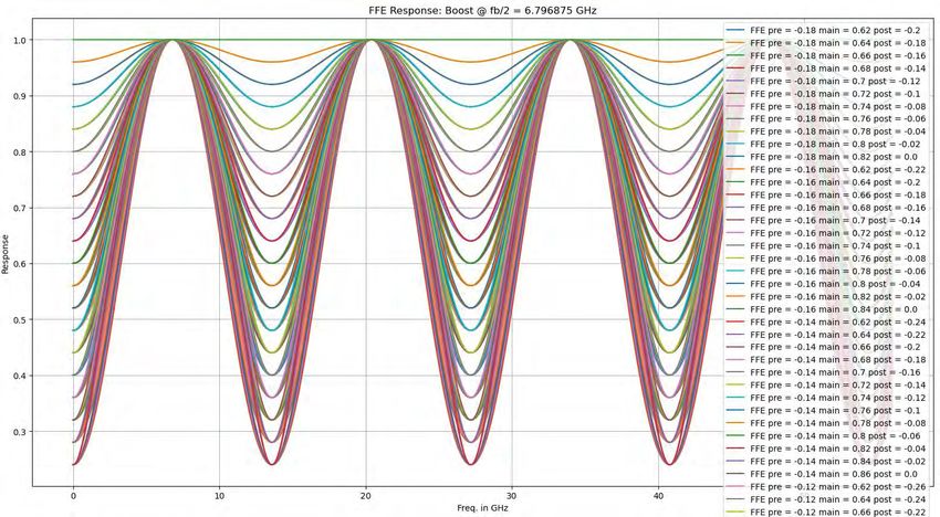
FFE: Feed Forward Equalizer

 FFE Sweep [4]
© Dassault Systèmes | 4/22/2021 | ref.: 3DS_Document_2020

 fb/2

 Sweep pre- and post-cursors.

 50
© Dassault Systèmes | 4/22/2021 | ref.: 3DS_Document_2020

51
 CTF Sweep
 [4]

 Sweep DC Gain
 CTF: Continuous Time Filter
FOM: Figure of Merit

 FOM Sweep [4]
© Dassault Systèmes | 4/22/2021 | ref.: 3DS_Document_2020

 FOM in dB

 sweep index for every
 combination of FFE and
 CTF setup.

 52
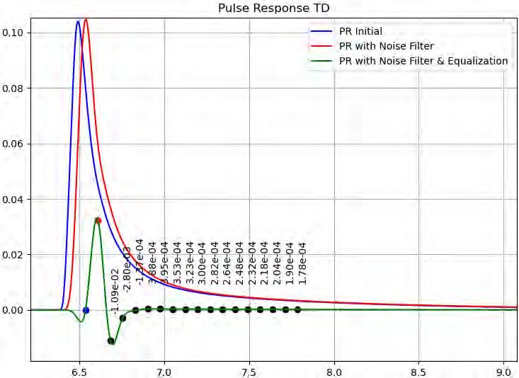
PR: Pulse Response
 FD: Frequency Domain

 Pulse Response (1/3) [4] TD: Time Domain
© Dassault Systèmes | 4/22/2021 | ref.: 3DS_Document_2020

 DFE taps
 Voltage in V

 Voltage in V/Hz
 Time in ns Frequency in GHz

 ➢ ISI and signal amplitude is significantly reduced by equalization.

 53
PR: Pulse Response
 FD: Frequency Domain

 Pulse Response (2/3) [4] TD: Time Domain
 Rx: Receiver
© Dassault Systèmes | 4/22/2021 | ref.: 3DS_Document_2020

 fb

 ➢ Rx Noise Filter removes FD response above fb. Rx
 ➢ Equalization makes FD response flatter. Filter
 54
PR: Pulse Response
 COM: Channel Operating Margin

 Pulse Response (3/3) [3][4]

 PR_COM
 PR_Transient Circuit Simulation_Foster
 PR_Transient Circuit Simulation_Standard
 PR_Transient Co-simulation Peak
 PR_COM
 PR_Transient Circuit Simulation_Foster
© Dassault Systèmes | 4/22/2021 | ref.: 3DS_Document_2020

 PR_Transient Circuit Simulation_Standard
 PR_Transient Co-simulation
 PR_COM
 PR_Transient Circuit Simulation_Foster
 PR_Transient Circuit Simulation_Standard
 PR_Transient Co-simulation

 Initial State

 Time in ns Time in ns Time in ns

 ➢ PR of COM can be validated by circuit simulations.
 ➢ As expected, standard macro model shows more noise at the peak and initial state
 than Foster because of the long propagation delay.
 ➢ Transient Co-simulation shows much less noise than macro modeling.
 55
PDF: Probability Density Function
 XT: Crosstalk

 Noise Terms & PDF [4]
© Dassault Systèmes | 4/22/2021 | ref.: 3DS_Document_2020

 Voltage in V
 ➢ No aggressor is simulated, so there’s no XT terms.
 ➢ Tx noise is larger than ISI, which is significantly reduced by equalization.
 ➢ PDF is normalized to 1.
 56
SR: Surface Roughness
 SC: Strong Coupling

 Comparison - Overview (1/6) ER: Epoxy Resin

 Models Surface Coupling Etching Epoxy Resin
 Roughness
 Ref. Trap45
 Ref. No Weak 90° No
© Dassault Systèmes | 4/22/2021 | ref.: 3DS_Document_2020

 SR Yes Weak 90° No
 SR Trap60
 SC No Strong 90° No

 SR+SC Yes Strong 90° No

 Trap45 No Weak 45° No
 SC ER

 Trap60 No Weak 60° No

 ER No Weak 90° Yes SR+SC ER+SC
 ER+SC No Strong 90° Yes

 57
SR: Surface Roughness
 SC: Strong Coupling

 Comparison - Overview (2/6) ER: Epoxy Resin

 COM in dB Difference to Ref in dB

 0.11
 0.82 0.85
 Ref. Trap45
 1.07
 1.58 1.5
 2.18
© Dassault Systèmes | 4/22/2021 | ref.: 3DS_Document_2020

 SR Trap60

 7.6 7.49
 6.78 6.75
 6.02
 6.53
 6.1 SC ER
 5.42

 SR+SC ER+SC

 Ref. SR SC SR+SC Trap45 Trap60 ER ER+SC
 58
SR: Surface Roughness
 SC: Strong Coupling
 ER: Epoxy Resin

 Comparison - Individual Factors (3/6) COM: Channel Operating Margin

 COM in dB Difference to Ref in dB

 0.11
 0.82 0.85
 Ref. Trap45
 1.07
 1.58 1.5
 2.18
© Dassault Systèmes | 4/22/2021 | ref.: 3DS_Document_2020

 SR Trap60

 7.6 7.49
 6.78 6.75
 6.02
 6.53
 6.1 SC ER
 5.42

 ➢ Surface roughness is the most critical
 factor to consider and causes about 1.5
 Ref. SR SC SR+SC Trap45 Trap60 ER+SC
 dB loss for COM.
 ER
 59
SR: Surface Roughness
 SC: Strong Coupling

 Comparison - SR (4/6) COM: Channel Operating Margin

 COM in dB Difference to Ref in dB

 0.11 ➢
 0.82 Strong coupling
 0.85
 Ref.
 1.07
 1.58 1.5
 2.18 doesn’t change the
© Dassault Systèmes | 4/22/2021 | ref.: 3DS_Document_2020

 results too much.
 SR
 ➢ Surface roughness has
 7.6 7.49
 more impact on COM
 6.78 for the
 6.53 strong
 6.75coupling
 6.02 6.1 SC
 5.42 case (in the sense 2.18
 > 1.58 + 0.11 dB).

 SR+SC

 Ref. SR SC SR+SC Trap45 Trap60 ER ER+SC
 60
COM: Channel Operating Margin

 Comparison - Etching (5/6)
 COM in dB Difference to Ref in dB

 0.11
 0.82 0.85
 Ref. Trap45
 1.07
 1.58 1.5
 2.18
© Dassault Systèmes | 4/22/2021 | ref.: 3DS_Document_2020

 Trap60

 7.6 7.49
 6.78 6.53 6.75
 6.02 6.1
 5.42
 ➢ Etch factor reduces
 COM about 1 dB.

 Ref. SR SC SR+SC Trap45 Trap60 ER ER+SC
 61
SC: Strong Coupling
 ER: Epoxy Resin

 Comparison - ER (6/6) COM: Channel Operating Margin

 COM in dB Difference to Ref in dB

 0.11 Ref.
 1.58
 ➢ Epoxy Resin 1.07
 0.82 0.85
 1.5
 between the diff.
 2.18
© Dassault Systèmes | 4/22/2021 | ref.: 3DS_Document_2020

 pair has also
 impact on COM.

 7.6 7.49 ➢ Epoxy Resin effect
 6.02
 is more6.78significant
 6.53 6.75
 6.1 ER
 5.42
 for designs with
 strong coupling (in
 the sense 1.5 > ER+SC
 0.85 + 0.11 dB)
 Ref. SR SC SR+SC Trap45 Trap60 ER ER+SC
 62
COM: Channel Operating Margin
 PR: Pulse Response

 Summary SR: Surface Roughness
 SC: Strong Coupling
 ER: Epoxy Resin
© Dassault Systèmes | 4/22/2021 | ref.: 3DS_Document_2020

 Ref. SC
 ➢ COM gives qualitative evaluation on passive channel designs in system level.

 ➢ COM PR can be validated by circuit simulations.

 ➢ SR effect is significant and should be considered according to COM analysis.

 ➢ If the diff. pair is strong coupled, effects of SR and ER can be more significant, which
 could be related to the field distribution.

 ➢ Etching and ER have also impact on the overall performance.
 63
References
 [1] IEEE Std. 802.3bj-2014.

 [2] G. Zhang, M. Huang and H. Zhang, “COM for PAM4 Link Analysis
© Dassault Systèmes | 4/22/2021 | ref.: 3DS_Document_2020

 – what you need to know”, EDI CON USA, 2018.

 [3] Dassault Systèmes, https://www.3ds.com/

 [4] J. D. Hunter, “Matplotlib: A 2D Graphics Environment”, Computing
 in Science & Engineering, vol. 9, no. 3, pp. 90-95, 2007

 64
© Dassault Systèmes | 4/22/2021 | ref.: 3DS_Document_2020

65
You can also read