Evaluating Common-Mode Voltage Based Trade-Offs in Differential-Ended and Single-Supplied Signal Conditioning Amplifiers
←
→
Page content transcription
If your browser does not render page correctly, please read the page content below
electronics
Article
Evaluating Common-Mode Voltage Based Trade-Offs in
Differential-Ended and Single-Supplied Signal
Conditioning Amplifiers
Marko Petkovsek *               and Peter Zajec

                                          Faculty of Electrical Engineering, University of Ljubljana, Trzaska 25, SI-1000 Ljubljana, Slovenia;
                                          peter.zajec@fe.uni-lj.si
                                          * Correspondence: marko.petkovsek@fe.uni-lj.si; Tel.: +386-14768862

                                          Abstract: This paper focuses on a differential voltage measurement in low-voltage automotive devices
                                          whose subunits are separated with a low-side safety switch. In contrast to conventional applications
                                          with high-side switches, a common-mode voltage (CMV) with negative polarity exists at the input of
                                          the signal conditioning circuitry. To overcome the shortage of dedicated integrated circuits capable
                                          of withstanding negative CMV, the paper investigates single- and two-stage differential circuits
                                          with single-supplied operational amplifiers to find a cost-optimized counterpart. In addition, the
                                          proposed procedure tunes the circuit parameters in such a manner to obtain the largest possible
                                          full-scale range at the output. Though, such optimization results in very uncommon values for gain
                                          and reference voltages. This issue is additionally evaluated for reference voltages that are either
                                          cost-effective or more easily accessible to increase the circuit feasibility. Since the impact of resistances
                                          on circuits’ behaviour could be diminished to a great extent using high-precision and matched pair

                                   resistors, the sensitivity analysis was investigated only for a reference voltage change. Furthermore, a
Citation: Petkovsek, M.; Zajec, P.        reversed termination of measured voltages results in a simplified reference voltage selection without
Evaluating Common-Mode Voltage            hindering circuits’ performance, proven by simulation and experimental results.
Based Trade-Offs in Differential-
Ended and Single-Supplied Signal          Keywords: voltage measurement; common-mode voltage; operational amplifier; differential-ended
Conditioning Amplifiers. Electronics      signal conditioning; low-side switch; high-power device
2021, 10, 1982. https://doi.org/
10.3390/electronics10161982

Academic Editor: Gaetano Palumbo          1. Introduction
                                                Hardly ever all subunits of an electronic device in a modern vehicle share the same
Received: 21 July 2021
                                          reference [1,2], i.e., ground potential. This situation calls for the implementation of signal
Accepted: 15 August 2021
Published: 17 August 2021
                                          conditioning circuits which merge all subunits into one functional part. Thus, their proper-
                                          ties, including gain, frequency bandwidth [3] and common-mode specifications, should
Publisher’s Note: MDPI stays neutral
                                          match the subunits’ input and output requirements.
with regard to jurisdictional claims in
                                                The ground difference depends on a relative position between a load and a main
published maps and institutional affil-
                                          switch that disconnects the main supply from the load. We differentiate two types of
iations.                                  applications, i.e., with a low-side and a high-side switch [4,5]. Whereas the control of
                                          the simplest loads is generally obtained through the high-side switch, more complex
                                          loads (DC/DC, DC/AC converters) incorporate either high- or low-side safety switches to
                                          disconnect the device from the power source in case of emergency [6]. A control scheme of
                                          a modern converter [7–9] contains numerous signal conditioning circuits [10,11], generally
Copyright: © 2021 by the authors.
Licensee MDPI, Basel, Switzerland.
                                          interfaced with a supervising microcontroller [12,13], to acquire currents and voltages and
This article is an open access article
                                          to supervise its operation. This case is addressed and clarified on a simplified converter
distributed under the terms and
                                          scheme (Figure 1) that consists of two subunits whose negative terminals are connected
conditions of the Creative Commons        through a low-side safety switch. The latter offers superior functionality in terms of
Attribution (CC BY) license (https://     increased safety over the high-side switch topology—not so much in a normal operation
creativecommons.org/licenses/by/          mode, but above all in case of a severe malfunction or even misuse of the device. For
4.0/).                                    instance, in case of an unintentional (outer) connection of uHP+ and uMG+ terminals only

Electronics 2021, 10, 1982. https://doi.org/10.3390/electronics10161982                                      https://www.mdpi.com/journal/electronics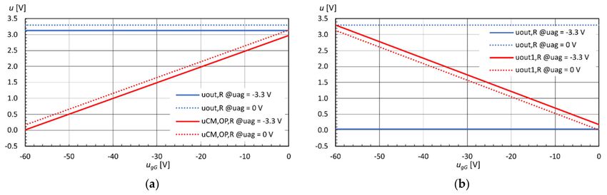
Electronics 2021, 10, 1982                                                                                                2 of 18

                             the low-side switch can prevent the power flow towards the load. For a reliable operation
                             of the high-power device, the designated voltages (umeas = {uag , uHP }) from an auxiliary
                             subunit must be acquired in all operation modes (start-up, failure, regular operation).
                             During these modes, the safety switch can take two discrete states (open, closed).

                             Figure 1. Simplified representation of an automotive device with a low-side safety switch.

                                    The magnitude of the common-mode voltage (CMV) at the input of the signal con-
                             ditioning circuit may, as a result, vary extensively and can change with a high slew rate
                             during low-side switch transitions. However, neither of both voltage phenomena restricts
                             the design of the conditioning circuit more than the fact that CMV has a negative polarity.
                             Besides, rare usage of low-side switch topologies causes a shortage of suitable and cost-
                             effective components for signal conditioning. It is worth mentioning that the highlighted
                             CMV issue is, in general, much easier to handle with dedicated ICs, featuring a build-in
                             isolation barrier (i.e., optic couplers) like in [14]. In automotive applications not exceeding
                             60 V, galvanic isolation is not mandatory. Thus, using the insulating couplers to transfer
                             logic signals between both stages would not be cost-effective.
                                    To overcome the shortage of dedicated ICs, we decided to analyse and evaluate some
                             custom-built circuits with operational amplifiers. OP amps with rail-to-rail input and
                             output (RRIO) specifications, whose CMV range not only equals but can also go beyond the
                             supply range, were supposed. Though, the range extends only for some tens of millivolts,
                             i.e., up to a 0.5 V increase beyond each supply rail is acceptable in case of a low voltage OP
                             amp ON NCV5230 [15] or an automotive TI TLV9001 [16].
                                    The paper is organized as follows: In Section 2, two single-supplied differential
                             conditioning circuits that are tolerant to negative CMV are investigated. For both circuits, a
                             procedure for circuit parameter determination is proposed to obtain the largest possible
                             full-scale range at the output for a given input voltage and CMV range. Section 3 provides
                             key simulation results for both circuits, followed by a possible approach for further circuit
                             parameter optimization focusing on the reference voltages used. Based on simulation
                             results, one signal conditioning circuit was selected and implemented in the laboratory
                             prototype of an advanced DC/DC converter for the automotive industry. Finally, in
                             Section 4, experimental results for voltage measurement in the DC/DC converter prototype
                             are given.

                             2. Common-Mode Voltage Restrictions in Single-Supplied Differential Circuits
                                  During the design of the signal conditioning circuit for systems like in Figure 1, three
                             voltage ranges (hereafter designated with capital U) must be considered: (1) full-scale
                             measuring voltage range (UFS,meas ) that yields to (2) full-scale output voltage range (UFS,out )
                             and, (3) common-mode voltage range (UCM ) that is applied between both subunits. Con-
                             sequently, diverse circuit topologies impose different CMV at the input of the chosen IC,
                             which in turn emphasizes the choice of an appropriate topology for the signal condition-
                             ing circuit.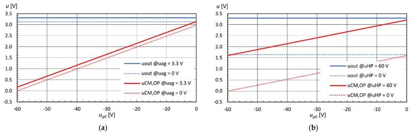
Electronics 2021, 10, 1982                                                                                           3 of 18

                                  In Figure 1, the measured voltages (uag , uHP ) are referenced against the “gnd” point;
                             in contrast, the measuring circuitry is terminated at the “GND” reference. The voltage
                             difference ugG between both sub-units ground potentials is not constant. It varies according
                             to the safety switch status from some mV, when the switch is closed, up to the magnitude
                             of uHP in its open state. Since in the latter situation, the level of measuring voltage can be
                             even three decades smaller than the ugG , its effect would not be adequately rejected at the
                             output of single-ended amplifier circuits.
                                  In such voltage circumstances, measuring circuitry with differential-ended topology
                             at the input front-end is a standard solution. Figure 2 shows its basic implementation with
                             a single supplied OP amp. A general approach representing the voltage circumstances at
                             the input terminals is applied. The measured voltage (umeas ) is substituted with a difference
                             between input voltages (uin + , uin − ), both being referenced against GND. In general, they
                             can be decomposed into a differential uDM

                                                              u DM = uin+ − uin− = umeas ,                              (1)

                             and a common-mode voltage uCM

                                                                           uin+ + uin−
                                                                   uCM =               ,                                (2)
                                                                                2
                             which excites both terminals with the same intensity. To reject its impact on the output
                             voltage (uout )

                                                              R2         R           R
                                                    uout =           1 + 4 uin+ − 4 uin− ,                         (3)
                                                           R1 + R2       R3          R3
                             the resistances R3 = R1 and R4 = R2 must be paired, resulting in

                                                                   R2               R
                                                          uout =      (u  − uin− ) = 2 umeas ,                          (4)
                                                                   R1 in+           R1

                             where a ratio R2 /R1 defines a gain G.

                             Figure 2. OP amp configured as a difference amplifier.

                                  By comparing the voltage notations in Figures 1 and 2, the derived CMV at the input
                             of the difference amplifier (uCM ) reveals its dependency on the switch state (i.e., ugG )

                                                                                  umeas
                                                                   uCM = u gG +         .                               (5)
                                                                                   2
                                  In (5), an infinitive rejection of CMV, provided by perfect resistance matching and an
                             ideal OP, is assumed. In contrast, the real OPs exhibit a finite capacity given by CMRR to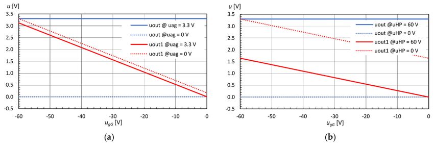
Electronics 2021, 10, 1982                                                                                           4 of 18

                             reject CMV (uCM,OP ) being present directly at the inputs of the operational amplifier. Its
                             correlation to the system-related CMV (uCM ) can be derived straightforwardly

                                                               R2                    R2         umeas
                                          uCM,OP = u+ =              u gG + umeas =         uCM +                       (6)
                                                             R1 + R2                R1 + R2        2

                             by assuming that the differential voltage (ud = u+ − u− ) tends to zero, i.e., by an infinite
                             differential gain (Ad ). To attain the assigned OP operation, the voltage at the input (6)
                             and output (4) must be within its input and output (IO) boundaries. According to (4), the
                             polarity of the measured voltage is preserved at the output side. Thus, input terminals
                             reversal, yielding in umeas < 0, is not allowed under any circumstance since a negative output
                             voltage in a single supplied OP amp is not attainable. In reality, the voltage boundaries
                             of individual OP families differ substantially. For further simplification, the IO voltage
                             boundaries match the positive (US+ ) and negative (0 V) rail supply voltage. Thus, an ideal
                             RRIO OP amp is assumed.
                                   As a result, the selected gain in (4) should agree with the preferred full-scale range
                             of umeas , not to violate the positive supply rail. On the other hand, fulfilling the input
                             restrictions relating to CMV (6) is often marginalized in practice, especially in single-
                             supplied OP circuits. Usually, this occurs because most users merely focus on CMV
                             rejection, i.e., CMRR capabilities [17,18]. The other cause might be that they do not
                             differentiate between the system-related CMV from one present on OP inputs. Therefore,
                             if resistances (R1 and R2 ) are selected merely to boost gain in (4), the CMV present at the
                             inputs of the OP could violate (6) limits. The OP operation is particularly jeopardized when
                             the ugG polarity is negative, and its magnitude prevails over umeas (6), driving the uCM,OP
                             towards the negative rail of the supply. In our case, the described situation occurs by a rule
                             whenever the safety switch is open.

                             2.1. Biased Differential Circuits
                                  An extra reference voltage uREF (Figure 3) resolves an inadequate tolerance to negative
                             CMV revealed in (6). It biases the noninverting input of the OP and consequently increases
                             its CMV away from the negative supply rail.

                                                                      R2          R1
                                                        uCM,OP =           u   +        u REF .                         (7)
                                                                    R1 + R2 in+ R1 + R2

                             Figure 3. OP amp configured as a biased difference amplifier.

                                  Considering R3 = R1 and R4 = R2 , the applied voltage at circuit’s input converts to uout

                                                           R2                         R
                                                  uout =      (uin+ − uin− ) + u REF = 2 umeas + u REF .                (8)
                                                           R1                         R1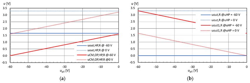
Electronics 2021, 10, 1982                                                                                                5 of 18

                                  Referring to (8) it is found that even in the worst-case scenario (umeas = 0 V,
                             ugG = ugG,max ), the CMV restriction at negative supply rail can be easily fulfilled such
                             to choose
                                                                                  R2
                                                               u∗REF = −u gG,max · .                                (9)
                                                                                  R1
                                  On the other side, the selected reference (9) confines the available output full-scale
                             voltage down to
                                                                      UFS,out = US+ − u∗REF ,                              (10)
                             and by inserting (9) into (8), consequently the gain as well
                                                                    ∗
                                                                R2                   US+
                                                                          =                       = G∗                     (11)
                                                                R1            UFS,meas − u gG,max

                                  The (11) is derived in such a way to prevent uout escaping beyond the positive rail
                             (US+ ) even in the worst-case scenario (UFS,meas , ugG = ugG,max ).

                             2.2. Two-Stage Difference Amplifiers
                                   To increase UFS,out across the entire rail to rail range of the OP (UFS,out = US+ ), a second
                             amplifier stage is required (Figure 4), transforming the output voltage of the first stage
                             (8) into
                                                           R22 R2                          R R
                                                uout = (      ( umeas + u REF ) − u REF ) = 2 22 umeas .                   (12)
                                                           R21 R1                          R1 R12

                             Figure 4. OP amp configured as a biased two-stage amplifier.

                                   In (12), the second stage gain R22 /R12 follows the same logic as in the first stage if
                             setting R12 = R32 and R22 = R42 . A complemented stage does not change uCM,OP at the input
                             of the first stage, whereas the second is inherently exposed solely to the positive uCM,OP .
                             For further evaluation, however, we have identified only the differential amplifier shown
                             in Figure 3 since the feature of the second stage in Figure 4 (12) is more easily implemented
                             within the MCU.
                                   A similar topology as in Figure 4 is implemented in a programmable gain difference
                             amplifier from [19], featuring very high CMRR, however offering only a limited gain
                             adjustment and—in case of using it with a single supply only, also a limited tolerance to
                             negative CMV.

                             2.3. Two-Stage Difference Amplifier Based on Instrumentation Amplifier Topology
                                 In general, in environments where a measurement path is exposed to electromagnetic
                             emissions [20–23] and severe CMV issues, instrumentation amplifiers are implemented as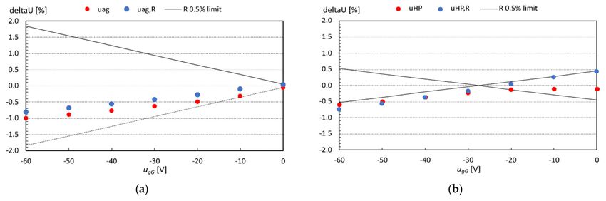
Electronics 2021, 10, 1982                                                                                           6 of 18

                             a rule [24,25]. They exhibit excellent CMRR features [26,27], however, they tolerate rather
                             modest CMV and their gains are higher than 1 [28], limiting their use in the presented case
                             as shown later on.
                                  In the following, an alternative two-stage amplifier is offered to emphasise the CMV
                             issue. Namely, since the uCM,OP (7) for circuit from Figure 3 varies correspondingly with
                             the applied CMV, the input crossover phenomena related to OP input topology [29] could
                             distort the output voltage. The alternative amplifier, seen in Figure 5 and adopted from [30],
                             page 418, has inherently a two-stage topology. Its output voltage can be expressed as

                                         R2 R F          RF               R2 R F              R + RG1 II RG2
                                 uout =         uin+ −      uin− − 1 +               u REF1 + F              u REF2   (13)
                                         R1 RG1         RG2               R1 RG1                RG1 II RG2

                             where a sign “II” denotes a parallel connection of resistances. To attain high CMRR (i.e.,
                             rejecting ugG ), the resistance quotients in front of uin + and uin - in (13) must be equal.
                             Subsequently, all four resistors should comply with

                                                                         R2  R
                                                                            = G1 .                                    (14)
                                                                         R1  RG2

                             Figure 5. A schematic of a two-stage difference amplifier.

                                The relations R1 = RG2 and R2 = RG1 should also be met, to assure the impedance
                             symmetry at the front-side of the amplifier. Thus, the (13) simplifies to

                                                      RF             RF              R + RG1 II RG2
                                             uout =       umeas −            u REF1 + F             u REF2 .          (15)
                                                      RG2         RG1 II RG2            RG1 II RG2

                                  The CMV at both OPs can be deduced straightforwardly

                                                                 u+,1 = uCM,OP1 = u REF1 ,                            (16)

                                                                 u+,2 = uCM,OP2 = u REF2 .                            (17)
                                   Thus, the reference voltages must be positive and their magnitude inside the supply
                             rail-to-rail levels to meet input OP restrictions. Since the same argument applies to uout
                             in (15), their magnitudes cannot be arbitrarily chosen. Namely, according to (15), the
                             CMV applied (i.e., ugG ) affect neither of the uCM,OP (16) nor (17), but it does affect the
                             uin + = umeas + ugG , and the output voltage of the first OP consequently

                                                                      R2            R2
                                                          uout1 = −      uin+ + 1 +      u REF1 .                     (18)
                                                                      R1            R1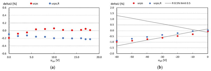
Electronics 2021, 10, 1982                                                                                             7 of 18

                                  Based on (18), two conditions should be met to comply with IO restrictions: (i) the
                             output voltage uout1 must not sink below zero even when the umeas matches its full-scale
                             value (UFS,meas ) and ugG = 0 V, and (ii) output voltage uout1 must be less or equal to positive
                             supply rail (US+ ) for the worst-case situation (umeas = 0 V, ugG = ugG,max ). After combining
                             both conditions, the first stage gain
                                                                 ∗
                                                             R2                   US+
                                                                       =                       = G1∗ .                  (19)
                                                             R1            UFS,meas − u gG,max

                             and the reference voltage u∗REF1 derive

                                                                                R2
                                                                  u∗REF1 =           U        .                         (20)
                                                                              R1 + R2 FS,meas

                                  Substituting uREF1 in (18) with (20) proves that uout1 does not violate negative supply
                             rail when worst-case combination (ugG = 0 V, umeas = umeas,max = UFS,meas ) is present.
                                  If uout = 0 V is to be achieved at umeas = 0 V, that is to transform (15) into

                                                                                 RF
                                                                       uout =        umeas ,                            (21)
                                                                                 RG2

                             the reference voltage uREF2 should fulfil the derived equilibrium

                                                          RF              R + RG1 II RG2
                                                                  u REF1 = F             u REF2 .                       (22)
                                                       RG1 II RG2            RG1 II RG2

                                  By rearranging (22), it is found that the preferred variables of the second stage
                             relate firmly
                                                                                 R∗F
                                                             u∗REF2 =                      u∗    .                      (23)
                                                                           R∗F + RG1 II RG2 REF1
                                  However, since the value of R1 = RG2 is already determined, the RF cannot be randomly
                             selected. It should also fulfil (21) deducing that voltages match their maximum allowed
                             value, summarising into
                                                                           US+
                                                                    R∗F =         R .                               (24)
                                                                          UFS,meas 1
                                 In contrast to derived equations, a trivial selection (uREF1 = uREF2 = 0) that comply
                             with (15) but fails to maintain (18) above negative supply rail at ugG = 0 V was rejected
                             from the beginning.

                             3. Simulation-Based Performance Review
                                   This section’s findings and discussion are grounded exclusively on results obtained
                             from simulations performed in LTspice and transferred into Excel for graphical representa-
                             tion. An ideal OP amp, with IO restriction matching the positive (US+ = 3.3 V) and negative
                             (0 V) rail supply voltage, was assumed. For elementary assessment in a steady-state con-
                             dition, such simulation is adequate to identify the trade-offs of the considered circuits.
                             Dynamic and frequency features of the signal conditioning circuits were thus put in the
                             second plan.
                                   Up to this point, we have established that proposed amplifier configurations, shown
                             in Figures 3 and 5, tolerate negative CMV. However, their features, including the achieved
                             full-scale range, parameter sensitivity, reference voltage feasibility and others are still to
                             be judged.
                                   For that purpose, two measured voltages with significantly different full-scale ranges
                             (UFS,ag = 3.3 V, UFS,HP = 60 V), denoted as blue bars in Figure 6, were applied to the input,
                             in addition to the CMV ranging from 0 V up to −60 V. Following the procedure described
                             in Section 2, we calculated circuits’ setpoints (Table 1) for specific voltage ranges, such that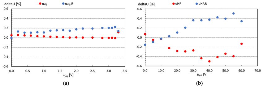
Electronics 2021, 10, 1982                                                                                                              8 of 18

                                     UFS,out preferably occupies the entire rail-to-rail supply voltage range (denoted as a grey
                                     bar in Figure 6).

                                      Figure 6. Designation of measured voltages in respect to gnd (in blue) and output voltage referenced
                                      to GND (in grey) (not in scale).

                             Table 1. Comparison between single- and two-stage difference amplifiers’ setpoints.

                                          Single-Stage                                           Two-Stage
                                      Difference Amplifier                                  Difference Amplifier
                                                           R2                                        R2             RF            RF
        Voltage Range                  u*REF        G* =   R1       u*REF1         u*REF2            R1             RG1           RG2
         UFS,ag = 3.3 V              3.128 V         0.0521       0.1635 V        0.1558           0.0521          19.185        1.0
         UFS,HP = 60 V               1.65 V          0.0275       1.6058 V        1.0802           0.0275            2.0        0.055

                                          Initially, the DC analysis was performed by sweeping the input voltages across the
                                     predefined full-scale range. Despite the CMV has the exact magnitude, Figure 7 reveals
                                     that the achieved output voltage in single- and two-stage amplifiers differs significantly.
                                     At umeas [p.u] = 1, the input voltage is in all three cases amplified to 3.3 V. Contrary, at the
                                     bottom margin umeas [p.u] = 0, we got 3.128 V and 1.65 V for amplifying the uag and uHP
                                     in the single-stage amplifier, respectively. At the same margin, the voltage in two-stage
                                     circuit is amplified to 0 V. The revealed full-scale readings are consequently consistent with
                                     calculated ones in Table 2. Both input voltages are given in per unit scale, with the base
                                     corresponding to their maximum values.

                                      Figure 7. Input-to-output correlation for two measured voltages and amplifier topologies.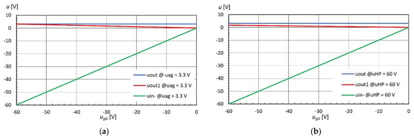
Electronics 2021, 10, 1982 9 of 18
Table 2. Comparison between calculated UFS,out for corresponding single- and two-stage ampli-
fiers’ setpoints.
Single-Stage Two-Stage
Difference Amplifier Difference Amplifier
Voltage Range
UFS ,out UFS,out1 UFS ,out
UFS,ag = 3.3 V 0.172 V 0.172 V 3.3 V
UFS,HP = 60 V 1.65 V 1.65 V 3.3 V
In the two-stage amplifier, the output voltage occupies the entire available range
(3.3 V), irrespective of neither the CMV nor the full-scale range of the input voltage. In
the single-stage amplifier, it is conversely limited into a smaller full-scale range. To make
matters even worse, the range narrows as the input voltage range decreases; evident at
UFS,ag = 3.3 V where the output range is reduced to 0.172 V. The latest also applies to
the first OP (UFS,out1 ) in the two-stage amplifier. In fact, the first stage must have the
same attenuation (Table 1) as the single-stage amplifier does, irrespective of constant CMV
presence at the OP inputs. Subsequently, the DC analysis was performed by sweeping the
CMV across its predefined full-scale range. It was conducted on both circuits providing
that the input voltages have been maintained on their margin values. Its purpose was
to identify any conceptual flaw made in Section 2, primarily focusing on CMV (uCM,OP )
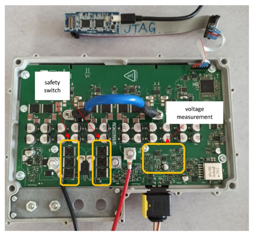
violation. The results are summarized in Figures 8–10.
Figure 8. Single-stage circuit output uout and uCM,OP vs. ugG for limit input values for measurement of: (a) uag ; (b) uHP .
Figure 9. Two-stage circuit outputs (uout and uout1 ) for limit input values vs. ugG for measurement of: (a) uag ; (b) uHP .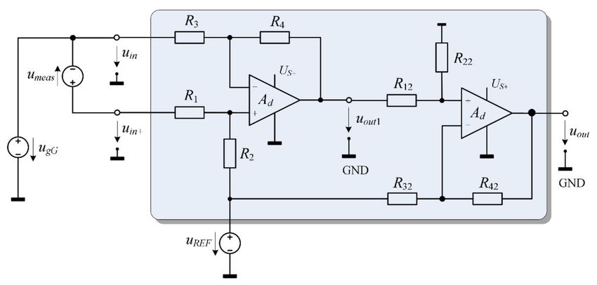
Electronics 2021, 10, 1982                                                                                                        10 of 18

      Figure 10. Two-stage circuit output uout and voltages at the second stage inputs vs. ugG for: (a) uag = 3.3 V; (b) uHP = 60 V.

                                        As can be seen, a stable voltage is identified at the output of the single-stage (Figure 8)
                                  and two-stage amplifier (Figure 9), regardless of the ugG variation. During its change,
                                  both figures demonstrate that the full-scale of each indicated voltage remains constant.
                                  Furthermore, the single-stage amplifier’s features do not depend on uCM,OP fluctuations
                                  as long as they remain within the supply margins (Figure 8). The same is valid in the
                                  two-stage variant (Figure 9), where the varying output voltage (uout1 ) is fed to the second
                                  OP. Inherently to the circuit in Figure 5, this change has no impact on CMV on the OP
                                  inputs, although the circuit terminals are subjected to large negative CMV, as emphasized
                                  in Figure 10. We want to recap this comparison referring back to Figure 7. It demonstrates a
                                  significantly smaller full-scale range for low input voltage uag , yet its measuring sensitivity
                                  S is roughly twofold compared to uHP .

                                                                               UFS,out
                                                                                        =S                                             (25)
                                                                               UFS,meas

                                  3.1. Parameter Sensitivity Analysis
                                        In general, during the circuit implementation, the discrepancy between calculated
                                  circuit parameters acquired from the proposed design procedure and those implemented
                                  regularly happens. The circuit parameters also deviate from their nominal values during
                                  the lifetime of a product. These deviations, which relate to production process tolerances,
                                  ageing mechanism, working environment temperature and other impacts, are usually
                                  neglected since they are small. However, in contrast to matched resistors, the voltage
                                  reference components exhibit a more significant deviation from their nominal specifications,
                                  particularly in terms of a temperature change [31,32]. Consequently, in the following
                                  analysis, we evaluated merely the impact of the reference voltages change while keeping
                                  the resistor values constant. We can justify this decision in two ways. First, the temperature
                                  coefficients of voltage reference components compared to those of matched pair resistors are
                                  higher—thus, a more significant effect was predicted. Furthermore, the pretty uncommon
                                  values displayed in Table 2 raised questions about reference voltage implementation, as
                                  well. Namely, although the shunt or series voltage references (such as TI LM4140 series [33])
                                  are commercially available in the sub 1 V range [34–38] in conjunction with a survey in [39],
                                  their nominal values still differ substantially from requested. An auxiliary circuit, such
                                  as a voltage divider combined with an OP amp-based voltage follower, can resolve this
                                  situation. Though, at the cost of simplicity and cost-effectiveness.
                                        Referring to a single-stage output voltage (8), any change of reference voltage ∆uREF
                                  causes the proportional change ∆uout at the output

                                                                             ∂uout
                                                                   ∆uout =          ·∆u REF = ∆u REF .                                 (26)
                                                                             ∂u REF
Electronics 2021, 10, 1982 11 of 18
In the same way, the two-stage output voltage (15) is evaluated concerning only
the change of the second stage’s reference voltage (the explanation is provided in the
following subsection).
∂uout R + RG1 II RG2
∆uout = ·∆u REF2 = F ·∆u REF2 = a·∆u REF2 (27)
∂u REF2 RG1 II RG2
where a represents the resistor’s ratio. Introducing a percentage change of the reference
(uREF ) and the output voltage
∆u REF
∆u REF% = ·100% (28)
u REF
∆uout
∆uout% = ·100%, (29)
uout
then using (26) and (27) for single-stage and two-stage circuits, respectively, the final
relations follow
u
∆uout% = REF ·∆u REF% (30)
uout
u
∆uout% = a· REF2 ·∆u REF2% . (31)
uout
According to (30) and (31), any voltage reference deviation causes a proportional
one in output voltage. Since its magnitude increases with an output voltage reduction, it
could severely compromise the measurement accuracy, as illustrated in Figure 11, where
a 1% reference voltage change is supposed, based on data from [29,30]. When uag is
amplified by single-stage circuit, the output error (30) is much larger (Figure 11a) compared
to uHP measurement. Remember that particular reference values (uREF = 3.128 V and
uREF = 1.65 V) define the minimum output value.
Figure 11. Percentage change of uout due to a 1% change in the reference voltage vs. the output voltage: (a) single-stage
circuit; (b) two-stage circuit.
In two-stage circuit, the output error also depends on the resistance ratio a, as defined
in (31). Since the ratio emerges already in general analysis, i.e., in (15) and (22) defining the
calculated reference voltages (Table 1), thus it turns out that the ratio is identical regardless
of the input voltage range. As a result, the voltage error (blue line in (Figure 11b), is
identical for both measured voltages. This non-intuitive statement is valid as (1) in each
case measured full-scale ranges are translated into identical rail-to-rail output voltage
range, and (2) since the percentage change is expressed according to output voltage uout .
In contrast, if we decide to replace the reference voltages, calculated from the proposed
procedure with cost-effective and/or accessible on the market, the term (a·uREF2 ) contrastsElectronics 2021, 10, 1982 12 of 18
for individual voltage measurements. To illustrate this, suppose that the designated
(labelled with des) references (uREF1 = uREF2 = 1 V) were applied instead of the calculated
given in Table 1. The resistor values corresponding to uag (Table 1) were recalculated
to sustain the permissible input and output voltage change for both OP amps resulting
in R2 /R1 = 0.039, RF /RG1 = 17.419 and RF /RG2 = 0.675, correspondingly. Under these
circumstances, the impact of a 1% reference voltage change is substantially higher (red
line in Figure 11b; for selected references valid only above 1 V) compared to the error for
proposed reference voltages (blue line). This, in general, depreciates the use of “randomly”
selected reference voltages. Despite the modification, the circuit reaches the positive rail at
the output at the same maximum measured voltage (uag = 3.3 V), as evident in Figure 12.
On the other hand, when uag is 0 V, the output voltage equals the reference voltage value
of 1 V. Consequently, the output range UFS,out becomes smaller than the one displayed in
Figure 9a, obtained as a result of the proposed procedure.
Figure 12. OP amp output uout vs. ugG for the measurement of uag and designated reference voltages.
If the output range UFS,out is not of a primary design concern, both references can be
chosen to fit the market offer considering the aforementioned drawbacks and OP amps’
IO specification.
3.2. Evaluating the Impacts of the Reversed Terminal Connection
The proposed procedure for parameter selection assumed the polarity of the measured
voltage, as depicted in Figure 1, where the positive terminal (labelled+) is connected to the
uin + terminal of the measurement circuit and negative (–) to uin - . However, considering the
(7) strictly from the mathematical point of view, a similar operation of the circuit (Figure 3)
is achieved with the reversed terminal connection, thus by applying negative voltage. To
preserve the proper operation, the reference voltages uREF must be changed. In a single-
stage circuit, uREF must, following (8) and (12), match positive supply rail US+ , irrespective
of the measured voltage (i.e., uag or uHP ). In contrast, uREF1 must be changed to zero for
the two-stage circuit while maintaining the same uREF2 values as before. The result of such
a change for both analysed circuits is for the measurement of uag visible in Figure 13 and
for the uHP in Figure 14. For both circuits and the measured voltage umeas = 0 V, the output
voltage equals uout = US+ . In contrast, for the maximum measured voltage, the output is
at the value initially defined with the uREF for a single-stage circuit (3.128 V and 1.65 V,
respectively), whereas for the two-stage circuit, the output is zero. Since the reversed
voltage connection imposes the voltage reference uREF1 = 0 V, the output voltage error (15)
can only depend on uREF2 , as defined (31).Electronics 2021, 10, 1982 13 of 18
Figure 13. Characteristic voltages vs. ugG for the reversed uag connection: (a) single-stage circuit; (b) two-stage circuit.
Figure 14. Characteristic voltages vs. ugG for the reversed uHP connection: (a) single-stage circuit; (b) two-stage circuit.
4. Experimental Results
A set of voltage measurements was performed on a laboratory prototype of an ad-
vanced 3.7 kW DC/DC converter (Figure 15), designed for the automotive industry to
validate the proposed calculation procedure. Its topology is not essential for the subject and
is adequately represented with the simplified scheme from Figure 1, with slight distinction
regarding the safety switch topology. Namely, as seen in Figure 15, a back-to-back switch is
implemented, where each set is composed of three N-channel MOSFET transistors. They
can disconnect the DC/DC converter from the high-power supply (UHP = 60 V in Figure 1)
during normal operation if so required (stand-by mode), but above all, in case of failure
or misuse of the device. UHP directly supplies the power stage and the control stage
with peripheral conditioning circuits. Their purpose is to measure different voltages in
an auxiliary circuitry. Since the safety switch separates both parts of the converter, the
conditioning circuits are subjected to a negative CMV when the switch is disconnected.
The simulation results for two analysed signal conditioning circuits that can handle the
negative CMV did not provide any strategic guidance or superiority favouring a specific
circuit, so we opted to implement the simpler scheme from Figure 3.
Circuit parameters were selected following the proposed procedure and are given in
Table 1. The selection of resistance values, however, is not entirely arbitrary. Namely, since
a voltage drop on R1 (and R3 = R1 ; Figure 3) could assume values as high as the power
supply uHP (60 V) or the ugG , the R1 value must be selected first. Furthermore, not only the
preferred power rating of the elements to be used (i.e., 0.125 W) but also a possible change
of resistances due to self-heating needs to be considered and then followed by R2 and R4
(being equal to R2 ) calculation. Their voltage drop is within the OP amp supply voltage
and therefore excessing the resistor power rating is not an issue here. In the prototype, theElectronics 2021, 10, 1982 14 of 18
value of R1 = 100 kΩ was selected for all cases, following with the calculation of R2 for
individual voltages based on data from Table 1 (all resistances used have a 0.5% tolerance).
Figure 15. DC/DC converter prototype fitted with single-stage conditioning circuits.
In Figure 16, experimental results for voltage error (labelled deltaU) on the full-scale
range of measured input voltages from 0 V to UFS,ag = 3.3 V and 0 V to UFS,HP = 60 V are
displayed for original (labelled uag and uHP ) and reversed polarity labelled (uag,R and uHP,R )
for ugG = 0 V. Next, both circuits were exposed to a changing negative CMV (ugG ) from 0 V
to −60 V, while preserving the measured voltages at their full-scale values of UFS,ag = 3.3 V
and UFS,HP = 60 V. As expected from Figure 8, the circuit output voltage should remain
constant (i.e., at 3.3 V) irrespective of the applied negative CMV, however, this is not
entirely true as seen from Figure 17. Otherwise, if the difference amplifier circuit is not
well balanced (i.e., R1 6= R3 and/or R2 6= R4 ), we could expect a significant discrepancy
compared to balanced (ideal) values. For comparison, Figure 17 also shows the calculated
worst-case voltage error margin vs. imposed negative CMV for resistances variation of
±0.5% (labelled R 0.5% limit).
Figure 16. Voltage error for original and reversed polarity of measured voltage on the nominal range: (a) for uag ; (b) for uHP .Electronics 2021, 10, 1982 15 of 18
Figure 17. Voltage error vs. ugG for original and reversed polarity of measured voltage: (a) for uag = 3.3 V; (b) for uHP = 60 V.
For practical reasons, required voltage references were obtained using a resistor di-
vider and an OP amp voltage follower in all presented cases. However, as discussed before
(results in Figures 13 and 14), connecting the measured voltage to the signal conditioning
circuit with the opposite polarity, the reference voltage selection can be simplified, since in
all cases the reference voltage should be set to a value of the positive supply rail (+3.3 V). In
this case, the output voltage of the signal conditioning circuit is reversed (i.e., for uag = 3.3 V,
the OP amp output is at 3.128 V and for uag = 0 V the OP amp output is at 3.3 V), so it
needs to be properly recalculated in the microcontroller where all measured voltages are
recalculated anyway. As seen from results, the reversed polarity does not hinder the circuits
performance, since it provides comparable results, yet with a voltage reference that is easier
available on the market.
To validate the proposed procedure for circuit parameter calculation, another voltage
(ucps ) from the auxiliary circuit with a maximum value of 18 V was also measured. For
this, we used a gain of G* = 0.0422 and u∗REF = 2.532 V, again resulting in a relatively low
voltage deviation from the calculated value for the input ucps and ugG change, as seen from
Figure 18a,b, respectively.
Figure 18. Voltage error for ucps measurement: (a) for the nominal range from 0 V to ucps = 18.0 V; (b) for ucps = 18.0 V vs. ugG .
5. Conclusions
In this paper, two signal conditioning circuits for a differential voltage measurement
based on single-supplied RRIO OP amps were analysed. With the proposed circuit’s
parameter calculation procedure, a voltage measurement with both differential circuits is
possible even if the measured voltage includes a CMV, varying in magnitude and polarity.Electronics 2021, 10, 1982 16 of 18
After simulation results for both circuits were compared, a decision for the circuit
that performs the signal conditioning task the best and is at the same time cost-effective
and easy to implement, is not that straight forward. On one side, a single-stage circuit
(Figure 3) could be superior compared to the two-stage circuit (Figure 5) on account of a
lower number of components. Also, with a reversed terminal connection, selecting the
reference voltage component is significantly simplified, since its value equals the positive
supply rail (US+ ). However, the output voltage does not occupy the whole available output
range, and the OP amp inputs are exposed to a changing CMV that could result in output
voltage distortion related to the input crossover issue.
On the other hand, selecting a two-stage circuit (Figure 5) offers a full-scale output
range for the full-scale measured voltage range as long as the proposed procedure for
parameter calculation is followed. With the two-stage topology, the CMV at OP amps
inputs is constant irrespective of the measured voltage or imposed CMV value. However,
for a practical implementation, a higher number of components—especially two reference
voltages—could be a decisive factor against the use of the circuit. It is true though, that
even with the reversed terminal connection, a certain simplification can be made, since the
reference voltage of the first stage should be set to a negative supply rail (GND), yet still
preserving the value of the reference voltage uREF2 .
As deduced from simulation results, a reversed connection of the measured voltage in
both cases simplifies the voltage reference selection. Especially in the single-stage circuit
experimentally verified, this could yield a significant cost decrease in mass production
since all system voltages are measured with signal conditioning circuits having the same
reference voltage and same electrical scheme. The only difference lies therefore in resistor
values, defining appropriate gains for individual measured voltages.
According to numerical data presented, the gain of the signal conditioning circuit is set
significantly below 0.1, which restricts the usage of dedicated ICs, such as instrumentation
amplifiers, since they are in general optimized for voltage gains higher than 1. On the
other hand, the use of difference amplifier ICs with built-in precision resistors offers only a
limited gain adjustment. That is why a custom-built difference amplifier has a vital role in
cost-sensitive applications regardless of the inherently lower common-mode rejection ratio
(CMRR). Consequently, a practical implementation of the signal conditioning circuit in the
high-power device relies not only on a selection of suitable circuits and their components
but also on a careful design of the printed circuit board.
Author Contributions: Conceptualization, M.P. and P.Z.; methodology, M.P.; validation, P.Z.; formal
analysis, M.P.; investigation, M.P. and P.Z.; resources, P.Z.; writing—original draft preparation, M.P.;
writing—review and editing, M.P. and P.Z.; visualization, M.P.; supervision, P.Z. Both authors have
read and agreed to the published version of the manuscript.
Funding: This research was supported in part by Slovenian Research Agency; Javna agencija
zaraziskovalno dejavnost Republike Slovenije, Bleiweisova cesta 30, 1000 Ljubljana, Slovenia, under
Grant L2619 »Advanced electronic power supply for automotive catalytic converter«.
Conflicts of Interest: The authors declare no conflict of interest. The funders had no role in the design
of the study; in the collection, analyses, or interpretation of data; in the writing of the manuscript, or
in the decision to publish the results.
References
1. Hoff, C.; Sirch, O. Elektrik/Elektronik in Hybrid- und Elektrofahrzeugen und Elektrisches Energiemanagement VII, 1st ed.; Expert-Verlag:
Renningen, Germany, 2016.
2. Cabizza, S.; Corradini, L.; Spiazzi, G.; Garbossa, G. Comparative Study of 48V-based Low-Power Automotive Architectures.
In Proceedings of the 2020 IEEE 21st Workshop on Control and Modeling for Power Electronics (COMPEL), Virtual, Aalborg,
Denmark, 9–12 November 2020; IEEE: New York, NY, USA, 2020; pp. 1–8. [CrossRef]
3. Lindenthaler, D.; Brasseur, G. Signal-Bandwidth Evaluation for Power Measurements in Electric Automotive Drives. IEEE Trans.
Instr. Meas. 2015, 64, 1336–1343. [CrossRef]
4. Texas Instruments. Basics of Power Switches; Application Report. Available online: https://www.ti.com/lit/an/slva927a/slva927
a.pdf (accessed on 15 July 2021).Electronics 2021, 10, 1982 17 of 18
5. Infineon. Smart High-Side Switches. Application Note. What a Designer Should Know. Available online: https:
//www.infineon.com/dgdl/Infineon-Application+Note-PROFET+12V-What+the+designer+should+know-AN-v01_00
-EN.pdf?fileId=5546d46259b0420a0159d5c957260d9c (accessed on 5 August 2021).
6. Deutschmann, B.; Winkler, G.; Kastner, P. Impact of Electromagnetic Interference on the Functional Safety of Smart Power Devices
for Automotive Applications. Elektrotechnik Informationstechnik. 2018, 135, 352–359. [CrossRef]
7. Carbajal-Retana, M.; Hernandez-Gonzalez, L.; Ramirez-Hernandez, J.; Avalos-Ochoa, J.G.; Guevara-Lopez, P.; Loboda, I.; Sotres-
Jara, L.A. Interleaved Buck Converter for Inductive Wireless Power Transfer in DC–DC Converters. Electronics 2020, 9, 949.
[CrossRef]
8. Wu, Y.; Ke, Y.A. A Novel Bidirectional Isolated DC-DC Converter with High Voltage Gain and Wide Input Voltage. IEEE Trans.
Power Electronics. 2021, 36, 7973–7985. [CrossRef]
9. Kumar, G.G.; Sai Krishna, M.V.; Kumaravel, S.; Babaei, E. Multi-Stage DC-DC Converter Using Active LC2D Network with
Minimum Component. IEEE Trans. Circuits Syst. II Express Briefs 2021, 68, 943–947. [CrossRef]
10. Zelin, L.; Gaofeng, P. Design of real time system to measure the voltage signal in high voltage power supply. J. Phys. Conf. Ser.
2021, 1887. [CrossRef]
11. Niklaus, P.S.; Bortis, D.; Kolar, J.W. Next Generation Measurement Systems with High Common-Mode Rejection. In Proceedings
of the 2018 IEEE 19th Workshop on Control and Modeling for Power Electronics (COMPEL), Padova, Italy, 25–28 June 2018;
pp. 1–8. [CrossRef]
12. Reverter, F. The Art of Directly Interfacing Sensors to Microcontrollers. J. Low Power Electron. Appl. 2012, 2, 265–281. [CrossRef]
13. Cheng, Y.; Sun, Y.; Li, X.; Dan, H.; Lin, J.; Su, M. Active Common-Mode Voltage-Based Open-Switch Fault Diagnosis of Inverters
in IM-Drive Systems. IEEE Trans. Ind. Electron. 2021, 68, 103–115. [CrossRef]
14. Dimitrov, B.; Collier, G.; Cruden, A. Design and Experimental Verification of Voltage Measurement Circuits Based on Linear
Optocouplers with Galvanic Isolation for Battery Management Systems. World Electr. Veh. J. 2019, 10, 59. [CrossRef]
15. ON Semiconductor. NCV5230. Available online: https://www.onsemi.com/pub/Collateral/NE5230-D.pdf (accessed on
15 July 2021).
16. Texas Instruments. TLV9001. Available online: https://www.ti.com/lit/ds/symlink/tlv9001.pdf (accessed on 15 July 2021).
17. Hornero, G.; Casas, O.; Pallàs Areny, R. Common mode response effects in differential measurements. AEU Int. J. Electron.
Commun. 2021, 128. [CrossRef]
18. Zhou, J.; Liu, J. On the measurement of common-mode rejection ratio. IEEE Trans. Circuits Syst. II Express Briefs 2005, 52, 49–53.
[CrossRef]
19. Analog Devices. AD628. Available online: https://www.analog.com/media/en/technical-documentation/data-sheets/AD628
.pdf (accessed on 15 July 2021).
20. Saponara, S.; Ciarpi, G. Electrical and Electromagnetic Measurements of an Inductorless DC/DC Converter. In Proceedings of the
I2MTC2017 Conference, Pisa, Italy, 22–25 May 2017. [CrossRef]
21. Saponara, S.; Ciarpi, G. Electrical, Electromagnetic, and Thermal Measurements of 2-D and 3-D Integrated DC/DC Converters.
IEEE Trans. Instr. Meas. 2018, 67, 1078–1090. [CrossRef]
22. Han, D.; Morris, C.T.; Lee, W.; Sarlioglou, B. A Case Study on Common Mode Electromagnetic Interference Characteristics of
GaN HEMT and Si MOSFET Power Converters for EV/HEVs. IEEE Trans. Transp. Electrif. 2017, 3, 168–179. [CrossRef]
23. Huang, K.; Liu, Z.; Zhu, F.; Zheng, Z.; Cheng, Y. Evaluation Scheme for EMI of Train Body Voltage Fluctuation on the BCU Speed
Sensor Measurement. IEEE Trans. Instr. Meas. 2017, 66, 1046–1057. [CrossRef]
24. Counts, L.; Kitchin, C. A Designer’s Guide to Instrumentation Amplifiers, 3rd ed.; Analog Devices: Wilmington, NC, USA, 2006;
pp. 154–196.
25. Azhari, S.J.; Fazlalipoor, H. CMRR in Voltage-Op-Amp-Based Current-Mode Instrumentation Amplifiers (CMIA). IEEE Trans.
Instr. Meas. 2008, 58, 563–569. [CrossRef]
26. Texas Instruments. INA117. Available online: https://www.ti.com/lit/ds/symlink/ina117.pdf (accessed on 15 July 2021).
27. Analog Devices. Instrumentation Amplifier Common-Mode Range: The Diamond Plot. Available online: https://www.analog.
com/media/en/technical-documentation/application-notes/AN-1401.pdf (accessed on 15 July 2021).
28. Texas Instruments. INA240 High- and Low-Side, Bidirectional, Zero-Drift, Current-Sense Amplifier with Enhanced PWM
Rejection. Available online: https://www.ti.com/product/INA240 (accessed on 7 August 2021).
29. Leon, E.; Barthel, R.; Alani, T. Zero-Crossover Amplifiers: Features and Benefits. Texas Instruments. Available online: https:
//www.ti.com/lit/an/sboa181a/sboa181a.pdf (accessed on 15 July 2021).
30. Mancini, R. Op Amps for Everyone; Texas Instruments: Dallas, TX, USA, 2002; p. 418.
31. Texas Instruments. Voltage Reference Selection Basics. Available online: https://www.ti.com/lit/wp/slpy003a/slpy003a.pdf
(accessed on 15 July 2021).
32. Maxim. Understanding Voltage-Reference Temperature Drift. Application Note. Available online: https://www.
maximintegrated.com/en/design/technical-documents/app-notes/4/4419 (accessed on 15 July 2021).
33. Texas Instruments. LM4140 High Precision Low Noise Low Dropout Voltage Reference. Available online: https://www.ti.com/
lit/ds/symlink/lm4140.pdf (accessed on 15 July 2021).
34. Analog Devices. Precision Series Sub-Band Gap Voltage Reference. Available online: https://www.analog.com/media/en/
technical-documentation/data-sheets/ADR130.pdf (accessed on 15 July 2021).Electronics 2021, 10, 1982 18 of 18
35. Ueno, K.; Hirose, T.; Asai, T.; Amemiya, Y. A 300 nW, 15 ppm/◦ C, 20 ppm/V CMOS Voltage Reference Circuit Consisting of
Subthreshold MOSFETs. IEEE J. Solid-State Circuits 2009, 44, 2047–2054. [CrossRef]
36. Magnelli, L.; Crupi, F.; Corsonello, P.; Pace, C.; Iannaccone, G. A 2.6 nW, 0.45 V Temperature-Compensated Subthreshold CMOS
Voltage Reference. IEEE J. Solid-State Circuits 2011, 46, 465–474. [CrossRef]
37. Liu, Y.; Zhan, C.; Wang, L.; Tang, J.; Wang, G. A 0.4-V Wide Temperature Range All-MOSFET Subthreshold Voltage Reference
with 0.027%/V Line Sensitivity. IEEE Trans. Circuits Syst. II Express Briefs 2018, 65, 969–973. [CrossRef]
38. Lee, I.; Sylvester, D.; Blaauw, D. A subthreshold voltage reference with scalable output voltage for low power IoT systems. IEEE J.
Solid-State Circuits 2017, 52, 1443–1449. [CrossRef]
39. Richelli, A. Low-Voltage Integrated Circuits Design and Application. Electronics 2021, 10, 89. [CrossRef]You can also read