Frequency-domain ultrafast passive logic: NOT and XNOR gates - Nature
←
→
Page content transcription
If your browser does not render page correctly, please read the page content below
ARTICLE
                  https://doi.org/10.1038/s41467-020-19544-9                OPEN

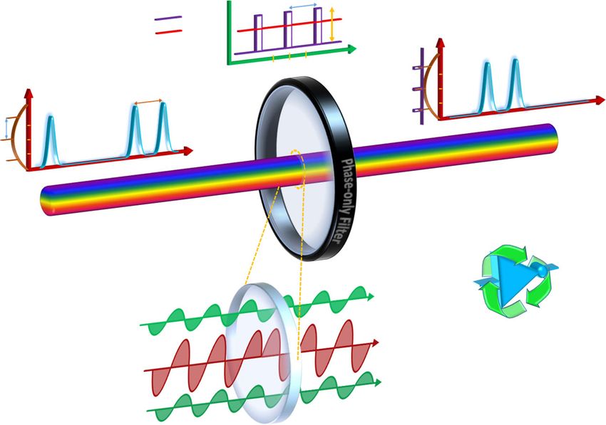
                  Frequency-domain ultrafast passive logic: NOT
                  and XNOR gates
                  Reza Maram 1,2,6, James van Howe1,3,6, Deming Kong4,5, Francesco Da Ros                                          4,   Pengyu Guan     4,

                  Michael Galili4, Roberto Morandotti 1, Leif Katsuo Oxenløwe4 & José Azaña                                         1✉
1234567890():,;

                  Electronic Boolean logic gates, the foundation of current computation and digital information
                  processing, are reaching final limits in processing power. The primary obstacle is energy
                  consumption which becomes impractically large, > 0.1 fJ/bit per gate, for signal speeds just
                  over several GHz. Unfortunately, current solutions offer either high-speed operation or low-
                  energy consumption. We propose a design for Boolean logic that can achieve both simul-
                  taneously (high speed and low consumption), here demonstrated for NOT and XNOR gates.
                  Our method works by passively modifying the phase relationships among the different fre-
                  quencies of an input data signal to redistribute its energy into the desired logical output
                  pattern. We experimentally demonstrate a passive NOT gate with an energy dissipation of ~1
                  fJ/bit at 640 Gb/s and use it as a building block for an XNOR gate. This approach is
                  applicable to any system that can propagate coherent waves, such as electromagnetic,
                  acoustic, plasmonic, mechanical, or quantum.

                  1 Institut National de la Recherche Scientifique (INRS) – Energie, Matériaux et Télécommunications, Montréal, QC H5A 1K6, Canada. 2 Fonex Data Systems

                  Inc., Montréal, QC H4S 1P6, Canada. 3 Department of Physics and Astronomy, Augustana College, Rock Island, IL 61201, USA. 4 Department of Photonics
                  Engineering, Technical University of Denmark, 2800 Lyngby, Denmark. 5 State Key Laboratory of Information Photonics and Optical Communications, Beijing
                  University of Posts and Telecommunications, 100876 Beijing, China. 6These authors contributed equally: Reza Maram, James van Howe.
                  ✉email: azana@emt.inrs.ca

                  NATURE COMMUNICATIONS | (2020)11:5839 | https://doi.org/10.1038/s41467-020-19544-9 | www.nature.com/naturecommunications                             1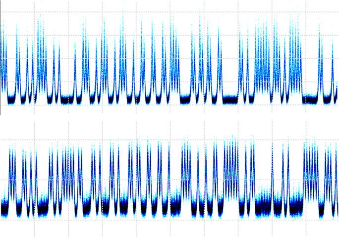
ARTICLE                                                                 NATURE COMMUNICATIONS | https://doi.org/10.1038/s41467-020-19544-9

B
       oolean logic gates are the building blocks of computation             based on spectral phase-only filtering28–30. Figure 1 shows the
       and digital information processing. However, current logic            operation principle of the fundamental NOT gate unit proposed
       gates, based on electronic transistors, are reaching physical         herein. In the illustrated example, an input temporal bit sequence
device limitations1–5. Unless fundamentally new technologies are             is encoded in a return-to-zero (RZ) on–off-keying (OOK) mod-
developed, growth in computational processing power, which has               ulation data format, where a binary “1” is represented by a high
increased exponentially over the past 50 years, may come to a halt           signal, a “0” as a low signal, and the data stream always returns to
within the next two decades. The primary obstacle is the imprac-             the zero-signal level momentarily after each bit. The time spacing
tical amount of energy consumed while switching transistors from             between consecutive bits, T, defines the bit period, which is
one logic state to another at high speeds2,3. Alternatives to elec-          inversely proportional to the bit rate of the data stream, B = 1/T.
tronic gates have been proposed using optics6–8, plasmonics9–12,             As shown in Fig. 1a, the frequency spectrum of the data signal
magnetism13,14, phononics15,16, and electromechanics17. Such                 consist of (i) a periodic set of strong components at discrete
gates operate by nonlinearity, similarly to an electronic transistor,        frequency locations that are spaced by the input bit rate B (i.e., the
or by splitting/combining the signal in linear interferometric               clock lines) and (ii) weaker components corresponding to the
devices. However, all proposed alternatives to date have yet to show         data that are distributed continuously along the signal spectrum
comparable, let alone superior, performance to current electronic            between the frequency clock lines. To implement the logical NOT
logic gates. They are either too slow or too energy inefficient, and          operation on the input digital signal, we selectively impart a phase
in some cases, they are based on unrealistic designs.                        shift of value π to just the frequency clock components of the
   Recent experimental work and toy models show gates operat-                signal using a phase-only, passive, linear filter. The clock fre-
ing at or near the Landauer Limit17,18 (six orders of magnitude              quencies are advanced in time compared to the remaining fre-
less energy consumption than current electronic complementary                quencies that represent the data, and the resulting interference
metal–oxide semiconductor (CMOS) gates); however, these                      pattern of all spectral components at the output is the exact
approaches pay their energy savings with decreased speed (five to             reversed bit sequence of the input. Figure 1b shows a detailed
ten orders of magnitude slower). More typical gate designs, which            explanation of how an amplitude-modulated signal can be com-
use nonlinearity, have shown Boolean logic operations at ultrafast           posed of clock and data components in both the time and fre-
speeds, however, at the price of high energy consumption19,20.               quency domain, and how a phase-only spectral filter can
   Caulfield et al., who coined the term “zero-energy” logic,                 implement the NOT gate operation.
devised many theoretical designs that they claimed could operate                The key to the conceptual understanding of the passive NOT
at high speed and consume no energy by using passive,                        gate is realizing that the electric field envelope of an amplitude-
linear interference21,22. However, closer investigation showed               modulated data signal can be thought of as the sum of a clock
that such gates were in fact energy hungry, and among other                  signal, cn (red), and a bipolar data component, dn (green). “0-
practical disadvantages, too physically large for realistic                  level” bits are simply the sum of negative data field amplitude
implementation23,24. Of many gate designs purporting to be                   pulses with positive amplitude clock pulses (which sum
“zero-energy,” “linear,” or “passive,” it is noteworthy that very            destructively), whereas “1-level” bits are the sum of positive data
few are entirely passive, and all consume some amount of energy.             field amplitude pulses with the clock (which sum constructively).
   Recently, truly passive Boolean logic gates have been demon-              By inverting the amplitude of the clock, bit levels that previously
strated using linear interference by coherent perfect absorption9            destructively interfered will then constructively interfere, and vice
and surface plasmon polaritons (SPP)10–12 in waveguide inter-                versa, resulting in the target NOT operation. In this process, only
ferometers. Though promising, like previous attempts at gate                 manipulation of the phase, not the intensity, is employed so that
design, these works have yet to show experimental demonstration              the input signal energy is entirely reused to form the output
of simultaneous low-energy consumption and high-speed                        logical pattern (except for practical insertion losses). Moreover, in
operation. Though both methods have potential to achieve                     contrast to previous NOT gate designs based on linear
high-speed operation, speeds have only been shown up to ~1 kHz               interference12, no additional energy other than the data stream
in proof-of-concept experiments.                                             itself is required for operation. A more detailed mathematical
   In this work, we demonstrate a fundamentally different                    derivation for each step of Fig. 1b is shown in Supplementary
approach to ultrafast, all-passive logic gate design. Whereas                Note 1. In the case of non-return-to-zero (NRZ) data signal, the
previous methods for passive gates introduce phase shifts onto               clock signal in Fig. 1b is replaced with a flat line (envelope of the
signal controls in the time-domain bit-by-bit for linear inter-              carrier) and the data signal does not return to zero for each bit
ference, our method imposes phase shifts in the frequency                    period. To apply the NOT gate operation for NRZ data, one
domain to spectral components of the signal, thereby processing              therefore simply applies the π phase shift to the central frequency
the entire data stream at once. We show ultrafast, low-energy-               tone (the carrier) instead of multiple clock tones.
consuming NOT and XNOR gate functions, which are directly                       Figure 2 shows the operating principle of a passive ultrafast
applicable to all-optical shift registers, packet header processing,         XNOR gate based on frequency-domain, passive NOT operation.
bit-error monitoring, modular arithmetic combinational and                   Here the gate (i.e., a Y-branch waveguide for the case of optical
multi-valued logic, scrambling/ciphering, and binary-to-                     signals) simply combines (i.e., sums) two input data streams with
quaternary encoding/decoding25–27. The speed of our gates is                 one of the inputs inverted by the frequency-domain, passive NOT
determined by the bandwidth of the spectral phase filter, whereas             gate. Whatever device is used as a combiner, it must be designed
energy consumption is only limited by the filter’s insertion loss,            so that there is no phase difference between the signals at the
allowing for both simultaneous high-speed operation and low-                 combination point other than the inverted clock of one of the
energy consumption. In a proof-of-concept experiment, a NOT                  data signals (Data A in this example). When we apply data signals
gate is demonstrated operating at a bit rate of 640 GB/s with an             to the proposed XNOR gate, we also assume that the two data
estimated energy dissipation of ~1 fJ/bit.                                   signals (Data A and Data B) have the same carrier frequency,
                                                                             same amplitude (for perfect operation), are coherent with each
                                                                             other, and have the same bit rate (which occurs, e.g., when Data A
Results                                                                      and Data B are derived from the same oscillator and the delay
Design of NOT and XNOR gates. The demonstrated logic gate                    between data streams A and B is within the oscillator’s coherence
designs are inspired by previous work on optical signal processors           time). The conceptual understanding of the frequency-domain

2                NATURE COMMUNICATIONS | (2020)11:5839 | https://doi.org/10.1038/s41467-020-19544-9 | www.nature.com/naturecommunications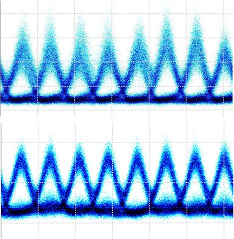
NATURE COMMUNICATIONS | https://doi.org/10.1038/s41467-020-19544-9                                                                                         ARTICLE

                           a                                                                     B
                                                                             Phase                                   Freq
                                                                             Amplitude
                                                                                                              Freq                          0   0
                                                                                                                                   1    1
                                                                                                                             0
                                                                                         fd1   fc fd2
                                       Freq
                                                                                                                            fd2
                                                                        1                                                   fc
                                                        0     1                                                             fd1                     Time
                                               1   0
                                                                   T
                                 B       fd2
                                          fc
                                         fd1                                   Time

                                                              fd2
                                                                                                                             Energy-preserving
                                                                                                                                 logic gate
                                                                  fc

                                                                   fd1

                           b                           Data
                             Power

                                                                   E-field

                                       1 1 0 1 0 0                                                   dn                           cn
                                                                                 Time                         Time                      Time
                                                              Power
                                                              (dBm)

                                                                                  Freq                        Freq                      Freq        FD
                                                       Data
                                                                                                                                  –cn
                               Power

                                                                   E-field

                                       0 0 1 0 1 1                                                   dn
                                               Time                              Time                         Time                      Time
                                                                  Power
                                                                  (dBm)

                                                                                  Freq                        Freq                      Freq

Fig. 1 The operation principle of the proposed frequency-domain zero switching-energy logic NOT gate. a A frequency-domain (FD), passive NOT gate
is implemented using a lossless passive all-pass (phase-only) linear filter. To perform the logical NOT operation on the digital (binary) input data signal, the
filter imparts a π phase shift to the clock components of the incoming coherent digital input with respect to the rest of the signal frequency spectrum.
Through this process, the output energy spectrum remains unchanged with respect to that of the input signal; however, in the time domain, the logic states
of the input bit sequence are reversed. fc (red) shows one of the frequency clock lines and fd1 and fd2 (green) represent arbitrary data frequencies. Note
how fc (red) is flipped in orientation at the output of the filter compared to fd1 and fd2. b Conceptual understanding of how amplitude-modulated data
streams can be thought of as a sum of their clock, cn (red), and data, dn (green), components. The difference between Data and its inverse, Data, is a π
phase shift (flipping in orientation) on clock frequency tones (red) with respect to the spectral data components (green). The summation of inverted clock
frequencies to the original data results in the NOT operation.

passive XNOR gate is similar to that of the proposed NOT gate.                                       works in this proposed implementation, which takes into account
We assume that the overall field amplitudes of Data A and Data B                                      the phase of data and clock signals to perform logical operations,
are each the sum of bipolar field amplitude data signals, dAn and                                     and should not be confused with a standard Boolean circuit
dBn, respectively (green), with their corresponding clocks, cn (red).                                diagram (i.e., in standard Boolean logic, A    þ B ≠ A XNOR B).
By inverting the clock of Data A (using a frequency-domain NOT                                       This gives the gate both advantages and disadvantages when
gate) and summing it with Data B at the combiner, the clock                                          compared to a standard Boolean XNOR device.
signals of Data A and Data B destructively interfere, leaving a field                                    One practical advantage of the proposed XNOR is that our
amplitude output, an, that is the sum of the input data field                                         technique outputs true Boolean “1” and “0” in the output
amplitude components, an = dAn + dBn. The resulting output                                           intensity, ideally giving infinite extinction between logic states
intensity |an|2 gives then the target XNOR operation. A more                                         when detecting power of the output data stream. This is in sharp
detailed mathematical derivation for the XNOR gate can be found                                      contrast to previous attempts of passive logic that combine two
in Supplementary Note 2.                                                                             Boolean inputs. For example, the interferometric gates shown by
   We emphasize that the NOT gate in the combiner in Fig. 2 is                                       refs. 10–12, even under ideal conditions, produce multiple power-
not a standard Boolean logic gate but rather the novel NOT gate                                      level outputs (i.e., the summation of data streams that represent
design proposed herein. Such a schematic for the XNOR only                                           an output “0” do not fully cancel to a zero level; likewise those

NATURE COMMUNICATIONS | (2020)11:5839 | https://doi.org/10.1038/s41467-020-19544-9 | www.nature.com/naturecommunications                                             3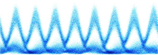
ARTICLE                                                                       NATURE COMMUNICATIONS | https://doi.org/10.1038/s41467-020-19544-9

                              Data A
                                                                                  dAn                  -cn

                                         E-field
               Power
                       1 0 1 0 0 1
                           Time                                              Time               Time
                                            dAn
                                                                                                                                                  A XNOR B

                                                                                                            E-field

                                                                                                                                    Power
                                                                cn
                                       Time              Time                FD                                                             1 0 0 1 0 1
                                                                                                                                                  Time
                                                                                                        an
                              Data B

                                         E-field
               Power

                                                                                                       Time                       Time
                       1 1 0 0 1 1
                          Time                                                                                                                     A XNOR B
                                       dBn                                    dBn                                     A   B   dAn   dBn      an
                                                                                                                                                  (Logic |an|2)
                                                                                                                      0   0   –1    –1       –2         1
                                                                cn                                     cn             0   1   –1     1       0          0
                                                                             Time               Time
                                       Time             Time                                                          1   0   1     –1       0          0
                                                                                                                      1   1   1      1       2          1

Fig. 2 The operation principle of the proposed frequency-domain zero switching-energy logic XNOR gate. Conceptual illustration of how a frequency-
domain (FD) passive NOT gate and a combiner can be used to implement an ultrafast passive XNOR operation. The FD NOT gate inverts the clock of Data
A (red), which when summed with Data B at the combiner destructively cancels the clock of Data B. The resulting output field, an, is simply the sum of the
data field amplitude of Data A, dAn, with the data field amplitude of Data B, dBn, an = dAn + dBn. The output intensity, |an|2, gives the XNOR operation. The
corresponding truth table is shown in the lower right-hand corner.

data streams that represent a “1” do not constructively interfere to                practice to maximize the entropy (average information) per bit
the same high-level output). Such multilevel output gates require                   and to minimize the overall probability of bit error31. See
lowering the threshold level that determines a “1” output and                       Supplementary Fig. 1 for a more detailed analysis on gate
raising the threshold level that determines a “0” output in order to                performance for an uneven distribution of “1s” and “0s.”
convert them into a true Boolean output. Unfortunately, this                           Figure 3a shows the input and output for NOT gate operation.
translates into the need for additional power-consuming non-                        The simulated gate applies periodic π phase shifts to clock
linear thresholding elements. Additionally, this also lowers the                    frequency components spaced by the input bit rate B = 640 GHz,
noise tolerance of the resulting gates and makes them much more                     where each phase shift occurs over a spectral linewidth of 8 GHz.
prone to logic state errors. We note that for physical systems                      The logic gate flips the state of the logical input signal (left) and
where the field/amplitude of the signal can be directly detected                     generates the reversed (NOT) logical output (right) with
(such as electronic or acoustic) our XNOR gate produces bipolar                     negligible distortions on the temporal shape of the individual
outputs such that three levels are allowed: “−2,” “0,” and “2” (see                 bits and eye diagram. Figure 3b shows simulated performance of
the truth table in Fig. 2 and the related mathematical derivations                  the XNOR using the same parameters as the NOT gate in Fig. 3a.
in Supplementary Note 2). In this case, thresholding will be                        Like the NOT gate, the proposed XNOR performs the target
needed for binary operations, which can be simply obtained by                       logical operation with negligible distortions on the temporal
detecting power (modulus squared of the amplitude) at the                           shape of the individual bits as well as the eye diagram.
receiver or by rectifying the signal before detection. However, in
some systems a bi-polar output may be desirable for denser
information coding.                                                                 Experimental demonstration of NOT gate. Next, we experi-
   One disadvantage to the XNOR gate proposed here is that its                      mentally demonstrate the frequency-domain, passive logic NOT
sensitivity to the phase implies that two XNORs cannot simply be                    gate design at a bit rate of 640 Gbit/s. For this purpose, the input
cascaded. Another is that the XNOR output is reduced by 3 dB                        signal is generated at optical wavelengths around 1537 nm to take
(compared to the combined input) since energy of the clock                          advantage of the speed offered by optics. Figure 4a shows a circuit
signals from Data A and Data B destructively interfere at the                       schematic of the experimental set-up. The input data signal, the
combiner output (shed into the higher order modes). However, in                     640 Gbit/s RZ data pulses, each with a 720-fs FWHM time width,
a 2 × 2 combiner, this clock energy could be retained and reused                    is generated by optical time division multiplexing (OTDM) of
for other operations downstream.                                                    64 × 10-Gbit/s OOK tributary data channels. Further details of
   To quantify gate performance, we numerically analyze the                         the experimental set-up can be found in Supplementary Fig. 2
NOT and XNOR gates in Fig. 3, which shows the input time trace                      and the Methods section. The input signal is then delivered to the
for 13 bits of a 128-bit random bit sequence (RBS), the output                      optical NOT gate unit. A commercial, programmable, spectral
time trace of each gate for the corresponding 13-bit input(s) and                   Waveshaper (WS) was used to produce the needed filtering. The
the input and output eye diagrams (insets). The eye diagram is a                    spectral clock components of the input signal, spaced by 640
graphical figure of merit for information processing systems and                     GHz, are phase-shifted by π with respect to the rest of the signal
is generated by superimposing successive bit waveforms, in order                    Fourier spectrum, as shown in Fig. 4b.
to form a composite image of the signal. The amount of eye                             Figure 4c, e show the measured temporal intensity traces of the
opening is related to the bit error rate (BER) and therefore system                 640 Gbit/s coherent RZ input data signal and the output of the
performance. A closed eye means the device or system between                        optical NOT gate, confirming inversion of the logical levels of the
the transmitter and the receiver is distorting bit levels of the input              input bit sequence. Figure 4d, f report the corresponding eye
signal so much that it introduces errors in the received data. In                   diagrams of the input and output data signals, showing an
our simulation, “1” bits are coded by Gaussian pulses, each with a                  observed improvement of the quality of the inverted data signal
400-fs full-width at half maximum (FWHM) time width, and the                        with respect to the input. This points out to a key additional
signal bit rate is chosen to be 640 Gbits/s. The input RBS has an                   feature of the proposed logic gate design, namely, its intrinsic
even distribution of “1s” and “0s”, which is the most common                        logic-level restoration capabilities, as numerically demonstrated

4                      NATURE COMMUNICATIONS | (2020)11:5839 | https://doi.org/10.1038/s41467-020-19544-9 | www.nature.com/naturecommunications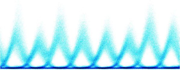
NATURE COMMUNICATIONS | https://doi.org/10.1038/s41467-020-19544-9 ARTICLE
a 1.2
Data A
1.2
NOT (Data A)
Power (a.u.)
Power (a.u.)
NOT gate
0.6 0.6
0 0
12 14 16 18 20 22 24 26 28 30 32 12 14 16 18 20 22 24 26 28 30 32
Time (ps) Time (ps)
b Data A Data B
1.2 1.2
Power (a.u.)
Power (a.u.)
0.6 0.6
0 0
XNOR gate
12 14 16 18 20 22 24 26 28 30 32 12 14 16 18 20 22 24 26 28 30 32
Time (ps) Time (ps)
A A XNOR B
A XNOR B 1.2
B
Power (a.u.)
0.6
FD
0
12 14 16 18 20 22 24 26 28 30 32
Time (ps)
Fig. 3 Demonstration of frequency-domain, passive logic NOT and XNOR gate through numerical simulation. a Left: 13 bits at 640 Gbit/s of a 128
random bit sequence (RBS) input to NOT gate, Right: NOT gate output of same 13 bits, insets: eye diagrams. b Top: 13 bits at 640 Gbit/s of two 128
random bit sequence inputs to the XNOR (Data A and Data B), Bottom right: corresponding XNOR output of 13 bits from logical operation of Data A and
Data B, insets: eye diagrams.
a Amplitude Phase
12.5 GHz Optical sampling scope
1.56 ps
f
640 Gb/s transmitter 640 GHz
1.56 ps
Time
Optical spectrum analyzer
640 GHz
WS 640 GHz
Spectrum PS
NOT gate
0
b 20
c Input 20 d 3.125 ps Input
6
Power (mW)
Power (dBm)/transmission (dB)
–10 10 10
3
–20
12.5 GHz
Phase (rad)
–30 0 0
0
–40
10 e Output 10 f Output
Power (mW)
–50 -3
–60 5 5
640 Gb/s
640 Gb/sWC WCRZRZ
–70 Phase filter
Phase Filter -6
Phase filter
Phase Filtermagnitude
Magnitude 0 0
–80
1545 1550 1555 1560 1565 1570 0 20 40 60 80 100 120 140 160 180 0 2 4 6 8 10 12
Wavelength (nm) Time (ps) Time (ps)
Fig. 4 Proof-of-concept demonstration of the frequency-domain zero switching-energy logic NOT gate. a Schematic of the experimental set-up.
Arrangement consisting of a 640-GHz optical RZ data transmitter, the logic NOT gate, and a receiver to measure the temporal waveform and spectrum of
the output signal. The logic NOT gate is implemented using an optical Waveshaper (WS) programmed to produce the needed phase-only linear filtering
specifications, i.e., a constant spectral amplitude and a spectral phase profile with π phase shifts periodically spaced by 640 GHz and with each shift
extending over a line-width of ~12.5 GHz (determined by the minimum frequency resolution of the WS). b Spectra of the coherent data signal input to and
output of the logic gate (they are overlapped), as well as spectral phase profile of the used phase filter (red). c, e Temporal traces of the 640 Gbit/s
coherent digital input data signal (c) and the inverted output data signal (e, synchronized with respect to the input for representation purposes). d, f Eye
diagram (overlapping the temporal signals over eight consecutive bit time periods) corresponding to the input and output data signals shown in plots c and
e, respectively.
NATURE COMMUNICATIONS | (2020)11:5839 | https://doi.org/10.1038/s41467-020-19544-9 | www.nature.com/naturecommunications 5
ARTICLE                                                                                                     NATURE COMMUNICATIONS | https://doi.org/10.1038/s41467-020-19544-9

                                                                                                                              Average sensitivity (dBm)
                                             –26               a                          Input

                         sensitivity (dBm)
                                                                                          Output                                –28.37             –27.91

                            Receiver
                                             –27

                                             –28

                                             –29

                                                          0            5       10    15       20     25           30       35         40       45       50        55        60        65
                                                                                                             Channel number

                                                                                                                         30
                                             Power (mW)
                                                          40       b                                      Input                   c                                    Output

                                                          30                                                             20
                                                                                          3.125 ps
                                                          20
                                                                                                                         10
                                                          10

                                                          –0                                                              0

                                                               0           2    4      6      8      10           12          0       2       4        6      8        10        12
                                                                                    Time (ps)                                                       Time (ps)

Fig. 5 Experimental results. a Receiver sensitivity, i.e., required average power at the output of the detection system to ensure a bit error rate (BER) 40.
for a given set-up, as well as the existence of any possible                                                           Degradation in the output signal quality does not become
analytical trend.                                                                                                      noticeable until the linewidth approaches ~300 MHz, giving an
   BER measurements were carried out by first demultiplexing the                                                        output Q = 5. Typical commercial optical telecom sources give
640 Gbit/s data sequence into 64 × 10-Gbit/s data signals using a                                                      spectral linewidths of 1–10 MHz while stabilized sources can
nonlinear optical loop mirror (NOLM), details of which are                                                             reach
NATURE COMMUNICATIONS | https://doi.org/10.1038/s41467-020-19544-9 ARTICLE
1.0 fJ/bit. For more details on our calculated energy consumption, phase shifts periodically spaced by 640 GHz. The total loss of our filter consists of
see Energy consumption metrics in the Methods section. For the device insertion loss of ~4.5 dB, plus an additional 3 dB of loss intentionally
added to the data frequency components between the clock tones. The latter is
comparison, the energy consumption for a simple nonlinear necessary because the π phase step-function that is imposed at the clock tones
optical logic gate is ~100 fJ/bit, while CMOS gate energy con- inherently introduces a corresponding step-function of loss of ~3 dB at these
sumption is ~0.1–1.0 fJ/bit (dominated by capacitive charging/ components. This undesired additional spectral amplitude variation of the
discharging of the gate interconnect wires)20,35,36. However, implemented filter is an intrinsic feature of the Waveshaper device that is used for
practical clock speeds per core for CMOS technology have satu- practical realization of the desired filtering function (ideally, a phase-only spectral
filtering function). We therefore need to induce this same value of loss (~3 dB)
rated in the range of 1–6 GHz2. Finally, the lowest energy con- along the remaining frequencies to achieve the desired flat spectral amplitude
sumption for a logic gate shown to date is ~0.1 aJ/bit17,37. Note, response of the filter. The nominal minimum bandwidth (frequency resolution) of
however, that such a low energy comes at a price of 1-kHz the Waveshaper is 10 GHz for implementation of amplitude filters and 12.5 GHz
operation. Our results show record performance for low-energy for implementation of phase filters. This latter specification determines the line-
width of the implemented phase shifts in our experiments. The spectral phase
operation in the ultrafast regime even though the specific phase response of the phase filter was measured with a 1.6-pm spectral resolution Optical
filter used for demonstrations is not optimal for energy dissipa- Vector Analyzer (Luna Technologies). It is worth noting that we use an active
tion. The energy consumption of our gate could be further programmable Waveshaper to emulate the target passive filter, i.e., a filter with a
minimized by lowering the energy of the incoming signal or by prescribed fixed spectral response. While the programming of the filter induces
additional loss, this is indeed not fundamental to the proposed concept. We note
reducing insertion losses in the linear optical filter through device that, for data signals with different bit rates, the spectral spacing of the π phase
and/or material optimization38. shifts needs to be reprogrammed to match the clock repetition rate. As described,
In summary, this work introduces a novel, design concept for the logic operation is implemented by the passive, linear all-pass filtering process
ultrafast logic gates based on passive, linear, phase-only filtering. itself.
Gate operation is fundamentally lossless and compatible with
ultrahigh bit-rate implementations. We experimentally show Detection and BER measurement. All temporal measurements are carried out
NOT gate operation using optical signals at 640 Gbit/s and a by a high-speed optical sampling oscilloscope (Exfo PSO-100) with a bandwidth
relative 1.0 fJ/bit energy consumption. We further use our NOT of 500 GHz. The measurements of the power spectra of the signals involved in
the reported experiments are carried out by an optical spectrum analyzer with a
gate to design an ultrafast, passive XNOR gate. Our concept is spectral resolution of 0.02 nm (Yokogawa AQ6370D). For the BER measure-
applicable to other physical systems (not just optical signals) ments, the 640-Gbit/s input and output signals are time-demultiplexed in a
that can propagate coherent waves. In terms of potential real- NOLM down to 10-Gbit/s signals. The NOLM operation is based on cross-phase
world device implementation, scaling the size of the phase filter modulation in a 50-m HNLF (zero-dispersion wavelength at 1545 nm, S = 0.015
ps/(nm2·km) at 1550 nm, and γ = 10.5 W−1·km−1) from OFS. The demulti-
will be critical. For optical signals, one could consider direct plexed 10-Gbit/s signal is detected by a 10-Gbit/s optically pre-amplified receiver
implementations based on integrated-waveguide Bragg gratings39 with a photodetector. The performance of the received signal is evaluated by a
or through SPP generation in subwavelength waveguide struc- 10-Gbit/s error analyzer (Anritsu MP1800A). For the receiver sensitivity mea-
tures9–12. Such circuits can be made with device lengths in the surements reported in Fig. 5, we used a BER threshold of 10−7 rather than the
standard BER threshold of 10−9; this was partly due to the relatively lower
micrometer range or even smaller. More generally, there may be quality of the input data sequence that could be generated for proof-of-concept
scaling advantages using our method with an entirely different experiments, Fig. 5b, c.
physics. With further development, phase-only, frequency-
domain filtering for logic gate design could offer solutions to
Energy consumption metrics. A fair comparison of energy consumption per bit
energy consumption and speed limitations in present computa- across logic gate methods throughout literature is difficult at best. Authors often
tion schemes. unintentionally underreport energy by not including amplifiers needed to boost the
signal before the logic gate (power that is often needed for nonlinear optical gate
operation) as well as fail to report energy consumed by active components in the
Methods gate that are continually powered, regardless of the presence of a signal20. We
OTDM signal generation and detection. We used a commercial Erbium-glass therefore use Tucker and Hinton’s work20 as a guide since they carefully and
pulsed laser in the transmitter to generate optical pulses at 1542 nm with a pulse- thoroughly analyze reported numbers from recent literature and add estimates of
width of 1.5 ps and 10 GHz repetition rate. Subsequently, the pulses are com- missing energy where authors have underreported numbers. In their comparison
pressed down to 720 fs by self-phase modulation in a 400-m-long section of work, Tucker and Hinton note that, for optical approaches, energy dissipated per
dispersion-flattened highly nonlinear fiber (HNLF, from OFS), and filtered with an bit scales inversely proportional to clock speed. In order to compare reported
optical band-pass filter (OBPF) (Koshin Kogaku KD-2396) at 1537 nm with a 3-dB energy consumption fairly, they normalize energy consumption of optical gates to a
bandwidth of 16 nm, see Supplementary Fig. 2. The pulses are then intensity reference clock of 100 GHz.
(OOK) modulated at the 10 Gbit/s base rate with a 27 −1 pseudo RBS data. The In our specific experiment, the method for gate operation is entirely passive.
modulated pulses are time-multiplexed in a passive fiber-based split-and-delay Therefore, the energy dissipated per bit by our NOT gate is determined solely
multiplexer (MUX) (Calmar BRM-T16) to constitute the 640 Gbit/s RZ OTDM by the input power, loss, and speed of the gate. For our set-up, the insertion
signal. Next, the 640 Gbit/s RZ OTDM signal is subsequently wavelength converted loss (IL) of the phase filter is IL = 7.5 dB (details provided above), which translates
using a polarization-rotating Kerr switch: the signal is first amplified using an into an estimated total energy loss per bit period of Eloss ¼ ðPin Pout ÞΔt ¼
Erbium-doped fiber amplifier (Keopsys EDFA) and coupled together with an Pin 1 10IL=10 Δt ¼ 6:4 fJ=bit, where Pin ≈ 5 mW and Pout ≈ 1 mW are the
amplified continuous-wave (CW) probe at 1559 nm in a 200-m HNLF (nonlinear average powers of the input and output data signals, respectively, and Δt ≈ 1.56 ps
coefficient: 10 W−1·km−1; zero dispersion wavelength: λ0 = 1552 nm; dispersion is the temporal bit period. Using 100 GHz as a reference clock to fairly compare our
slope: S = 0.011 ps/(nm2·km)). At the fiber output, a polarizer is placed with its axis method to those in ref. 20, we find a normalized energy consumption of our gate to
orthogonal to the CW light. The polarization of the data is 45° with respect to the be Enorm ¼ Eloss ´ ðfref =fclock Þ = 6.4 fJ/bit × (100 GHz/640 GHz) = 1.0 fJ/bit. We
polarizer. The CW light is blocked by the polarizer when the data signal is a “0” compare this number to the energy consumption of single, simple optical and
level bit. When the data signal is a “1” level bit, the Kerr effect in the fiber generates CMOS gates, which dissipate ~100 and ~0.1−1.0 fJ/bit, respectively20,35,36. To give
birefringence between the polarization direction of the data signal and its ortho- more context, we also compare this to ultralow energy consumption shown by a
gonal direction. Therefore, in this case, the state of polarization of the CW light will recent electromechanical method17,32, which demonstrated a dissipation of ~100
rotate due to the induced birefringence, thus passing through the polarizer. As a kBT/bit, i.e., ~0.1 aJ/bit, but at a significantly reduced speed of ~1 KHz.
result, the phase-uncorrelated OTDM data signal switches the CW light, and a
pulse-to-pulse phase-correlated signal is generated at the CW light wavelength.
Before wavelength conversion, an OBPF with bandwidth of 23 nm is used to filter Data availability
out the amplified spontaneous emission introduced by the EDFAs. We emphasize The datasets generated during and/or analyzed during the current study are available
that a coherent data signal is required for implementation of the proposed logic from the corresponding author on reasonable request.
gate concept based on phase-only (all-pass) linear filtering.
Code availability
Phase-only filter. A line-by-line pulse shaper (Finisar Waveshaper 4000S) has The computer simulation code used to report expected results, and compare
been programmed to produce the needed linear filtering response, namely, a experimental data to theory, is available from the corresponding author on reasonable
constant spectral amplitude response and a spectral phase response profile with π request.
NATURE COMMUNICATIONS | (2020)11:5839 | https://doi.org/10.1038/s41467-020-19544-9 | www.nature.com/naturecommunications 7ARTICLE NATURE COMMUNICATIONS | https://doi.org/10.1038/s41467-020-19544-9
Received: 3 July 2020; Accepted: 15 October 2020; 32. Pudo, D. & Chen, L. R. Simple estimation of pulse amplitude noise and timing
jitter evolution through the temporal Talbot effect. Opt. Express 15, 6351–6357
(2007).
33. Maram, R., van Howe, J., Li, M. & Azaña, J. Noiseless intensity amplification
of repetitive signals by coherent addition using the temporal Talbot effect.
Nat. Commun. 5, 5163 (2014).
References 34. Maram, R. et al. Demonstration of input-to-output gain and temporal noise
1. Semiconductor Industry Association. 2015 International Technology Roadmap mitigation in a Talbot amplifier. IEEE Photonics Technol. Lett. 30, 665–668
for Semiconductors (ITRS), www.itrs2.net (2015). (2018).
2. Markov, I. L. Limits on fundamental limits to computation. Nature 512, 35. Miller, D. A. B. Attojoule optoelectronics for low-energy information
147–154 (2014). processing and communications. J. Light. Technol. 35, 346–396 (2017).
3. Ball, P. Computer engineering: feeling the heat. Nature 492, 174–176 (2012). 36. Hooke, T. B. Power and technology scaling into the 5 nm node with stacked
4. Cavin, R. K., Lugli, P. & Zhirnov, V. V. Science and engineering beyond nanosheets. Joule 2, 1–4 (2018).
Moore’s Law. Proc. IEEE 100, 1720–1749 (2012). 37. Kish, L. B. Comments on “Sub-kBT micro-electromechanical irreversible logic
5. Chien, A. A. & Karamcheti, V. Moore’s Law: the first ending and a new gate”. Fluct. Noise Lett. 15, 1620001 (2016).
beginning. Computer 46, 48–53 (2013). 38. Yang, W. et al. High speed optical phased array using high contrast grating all-
6. Willner, A. E., Khaleghi, S., Chitgarha, M. R. & Yilmaz, O. F. All-optical signal pass filters. Opt. Express 22, 20038–20044 (2014).
processing. J. Light Technol. 32, 660–680 (2014). 39. Bazargani, H. P., Burla, M., Chrostowski, L. & Azaña, J. Photonic Hilbert
7. Ma, S. et al. Low-photon-number optical switch and AND/OR logic gates transformers based on laterally apodized integrated waveguide Bragg gratings
based on quantum dot-bimodal cavity coupling system. Sci. Rep. 6, 19001 on a SOI wafer. Opt. Lett. 41, 5039–5042 (2016).
(2016).
8. Kita, S., Nozaki, K., Takata, K., Shinya, A. & Notomi, M. Silicon linear optical
logic gates for low-latency computing. In Conference on Lasers and Electro-
Acknowledgements
This work was supported in part by the Natural Sciences and Engineering Research
Optics (2018) (Optical Society of America, Washington, D.C., 2018).
Council of Canada (NSERC) and the Fonds de recherche du Québec - Nature et tech-
9. Papaioannou, M., Plum, E., Valente, J., Rogers, E. T. F. & Zheludev, N. I. All-
nologies (FRQNT). R. Maram acknowledges financial support from the Ministère de
optical multichannel logic based on coherent perfect absorption in a
l’Éducation, du Loisir et du Sport (MELS) du Québec through the Merit Scholarship
plasmonic metamaterial. APL Photonics 1, 090801 (2016).
Program for Foreign Students. DTU authors acknowledge the European Research
10. Davis, T. J., Gomez, D. E. & Roberts, A. Plasmonic circuits for manipulating
Council (ERC) for supporting the SOCRATES project, DFF Sapere Aude Advanced
optical information. Nanophotonics 6, 43–59 (2017).
Grant NANO-SPECs and SPOC, a DNRF Centre of Excellence.
11. Sang, Y. et al. Broadband multifunctional plasmonic logic gates. Adv. Opt.
Mater. 6, 1701368 (2018).
12. Fu, Y. et al. All-optical logic gates based on nanoscale plasmonic slot
waveguides. Nano Lett. 12, 5784–5790 (2012). Author contributions
13. Bhowmik, D., You, L. & Salahuddin, S. Spin Hall effect clocking of R. Maram, J.V.H., and J.A. developed the concept. R. Maram carried out the theoretical
nanomagnetic logic without a magnetic field. Nat. Nanotechnol. 9, 59–63 derivations, numerical validations, and data analysis. R. Maram, D.K., F.D.R, P.G.,
(2014). and M.G. performed the experiments. L.K.O. provided management oversight of
14. Chumak, A. V., Serga, A. A. & Hillebrands, B. Magnon transistor for all- the experiments. All authors contributed to the writing of the manuscript. J.A. and
magnon data processing. Nat. Commun. 5, 4700 (2014). R. Morandotti provided management oversight for the project.
15. Maldovan, M. Sound and heat revolutions in phononics. Nature 503, 209–217
(2013).
16. Li, N. et al. Colloquium: Phononics: manipulating heat flow with electronic Competing interests
analogs and beyond. Rev. Mod. Phys. 84, 1045–1066 (2012). The authors declare no competing interests.
17. López-Suárez, M., Neri, I. & Gammaitoni, L. Sub-k B T micro-
electromechanical irreversible logic gate. Nat. Commun. 7, 12068 (2016).
18. Bérut, A. et al. Experimental verification of Landauer’s principle linking Additional information
Supplementary information is available for this paper at https://doi.org/10.1038/s41467-
information and thermodynamics. Nature 483, 187–189 (2012).
020-19544-9.
19. Miller, D. A. B. Are optical transistors the logical next step? Nat. Photonics 4,
3–5 (2010).
Correspondence and requests for materials should be addressed to J.Aña.
20. Tucker, R. S. & Hinton, K. Energy consumption and energy density in optical
and electronic signal processing. IEEE Photonics J. 3, 821–833 (2011).
Peer review information Nature Communications thanks Juerg Leuthold and the other
21. Caulfield, H. J., Zavalin, A. & Lei, Q. Zero-energy optical logic: can it be
anonymous reviewer for their contribution to the peer review of this work.
practical? J. Supercomput. 62, 681–688 (2012).
22. Caulfield, H. J. & Dolev, S. Why future supercomputing requires optics. Nat.
Reprints and permission information is available at http://www.nature.com/reprints
Photonics 4, 261–263 (2010).
23. Tucker, R. S. The role of optics in computing. Nat. Photonics 4, 405 (2010).
Publisher’s note Springer Nature remains neutral with regard to jurisdictional claims in
24. Miller, D. A. B. The role of optics in computing. Nat. Photonics 4, 406 (2010).
published maps and institutional affiliations.
25. Wong, W. M. & Blow, K. J. Design and analysis of an all-optical processor for
modular arithmetic. Opt. Commun. 265, 425–433 (2006).
26. Chattopadhyay, T., Roy, J. N. & Chakraborty, A. K. Polarization encoded all-
optical quaternary R-S flip-flop using binary latch. Opt. Commun. 282, Open Access This article is licensed under a Creative Commons
1287–1293 (2009). Attribution 4.0 International License, which permits use, sharing,
27. Säckinger, E. Analysis and Design of Transimpedance Amplifiers for Optical adaptation, distribution and reproduction in any medium or format, as long as you give
Receivers (Wiley, New Jersey, 2017). appropriate credit to the original author(s) and the source, provide a link to the Creative
28. Maram, R., Kong, D., Galili, M., Oxenløwe, L. K. & Azaña, J. Ultrafast all- Commons license, and indicate if changes were made. The images or other third party
optical clock recovery based on phase-only linear optical filtering. Opt. Lett. material in this article are included in the article’s Creative Commons license, unless
39, 2815–2818 (2014). indicated otherwise in a credit line to the material. If material is not included in the
29. Maram, R., Kong, D., Galili, M., Oxenlowe, L. K. & Azana, J. Passive linear- article’s Creative Commons license and your intended use is not permitted by statutory
optics 640 Gbit/s logic NOT gate. In 2015 Optical Fiber Communications regulation or exceeds the permitted use, you will need to obtain permission directly from
Conference and Exhibition (OFC) 1–3 (IEEE, New York, 2015). the copyright holder. To view a copy of this license, visit http://creativecommons.org/
30. Maram, R., Kong, D., Galili, M., Oxenløwe, L. K. & Azaña, J. 640 Gbit/s licenses/by/4.0/.
return-to-zero to non-return-to-zero format conversion based on optical
linear spectral phase filtering. Opt. Lett. 41, 64–67 (2016).
31. Yu, F. T. S. Entropy and Information Optics: Connecting Information and Time © The Author(s) 2020
(CRC Press, Florida, 2017).
8 NATURE COMMUNICATIONS | (2020)11:5839 | https://doi.org/10.1038/s41467-020-19544-9 | www.nature.com/naturecommunicationsYou can also read


