High Sensitivity Flexible Electronic Skin Based on Graphene Film - MDPI
←
→
Page content transcription
If your browser does not render page correctly, please read the page content below
sensors
Article
High Sensitivity Flexible Electronic Skin Based on
Graphene Film
Xiaozhou Lü 1 , Jiayi Yang 1, *, Liang Qi 1 , Weimin Bao 1 , Liang Zhao 2 and Renjie Chen 3
 1  The School of Aerospace Science and Technology, Xidian University, Xi’an 710071, China; lxz@uw.edu (X.L.);
    lqi_1@stu.xidian.edu.cn (L.Q.); baoweimin@cashq.ac.cn (W.B.)
 2  Science and Technology on Space Physics Laboratory, Beijing 100076, China; imu-zhl@163.com
 3  Beijing Key Laboratory of Environmental Science and Engineering, School of Chemical Engineering and the
    Environment, Beijing Institute of Technology, Beijing 100081, China; chenrj@bit.edu.cn
 * Correspondence: yang.jiayi@stu.xidian.edu.cn

 Received: 26 November 2018; Accepted: 29 January 2019; Published: 15 February 2019

 Abstract: Electronic skin with high sensitivity, rapid response, and long-term stability has great
 value in robotics, biomedicine, and in other fields. However, electronic skin still has challenges
 in terms of sensitivity and response time. In order to solve this problem, flexible electronic skin
 with high sensitivity and the fast response was proposed, based on piezoresistive graphene films.
 The electronic skin was a pressure sensor array, composed of a 4 × 4 tactile sensing unit. Each sensing
 unit contained three layers: The underlying substrate (polyimide substrate), the middle layer
 (graphene/polyethylene terephthalate film), and the upper substrate bump (polydimethylsiloxane).
 The results of the measurement and analysis experiments, designed in this paper, indicated that the
 flexible electronic skin achieved a positive resistance characteristic in the range of 0 kPa–600 kPa,
 a sensitivity of 10.80 Ω/kPa in the range of 0 kPa–4 kPa, a loading response time of 10 ms, and a spatial
 resolution of 5 mm. In addition, the electronic skin realized shape detection on a regular-shaped object,
 based on the change in the resistance value of each unit. The high sensitivity flexible electronic skin
 designed in this paper has important application prospects in medical diagnosis, artificial intelligence,
 and other fields.

 Keywords: aerospace; flexible sensor; micro-pressure measurement; sensitivity compensation

1. Introduction
      Electronic skin is an electronic system which can simulate the perception of human skin [1–3].
As electronic skin has the ability to detect pressure [4–9], it has received widespread attention in
the fields of human health monitoring [10–12], medical diagnosis [13], biological research [14,15],
artificial intelligence, and other fields [10,16]. In order to simulate the human skin pressure sensing
system, electronic skin should be able to measure different pressure ranges (less than 10 kPa,
and 10–100 kPa), and has the characteristics of high sensitivity and a fast response time [10].
Various approaches have been used to develop electronic skin. The most common working principles
of electronic skin are piezocapacitance and piezoresistance. Capacitive electronic skin usually has
high sensitivity. Joo et al. presented a pressure sensitive transistor array, based on a carbon nanotube
(CNT) silver nanowire. The array had a sensitivity of 9.9 kPa−1 in the range of 0–0.6 kPa and could
be easily integrated into a wearable system [17]. Lipomi et al. designed an electronic skin which
can measure pressure and tension. This electronic skin could bear up to 150% of the strain, and had
conductivity under the tensile state as high as 2200 S/cm, in the range of 0–50 kPa with a sensitivity of
0.004 kPa−1 [18]. Although the capacitive electronic skin had high sensitivity, it was vulnerable to stray
capacitance and parasitic capacitance, the measurement of the electronic skin was unstable, and the

Sensors 2019, 19, 794; doi:10.3390/s19040794                                    www.mdpi.com/journal/sensors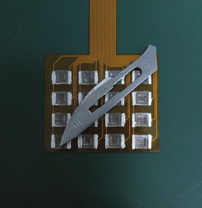
Sensors 2019, 19, 794                                                                                2 of 11

measuring range was small. Electronic skin based on resistance has the advantages of high sensitivity,
good chemical stability, and a simple manufacturing process. Yu et al. proposed a high-performance
piezoresistive electronic skin using CNT and polydimethylsiloxane (PDMS) [19]. The electronic skin
could measure pressure in the range of 7–50 kPa, and had a response speed of 10 ms and good stability.
However, the sensitivity of the electronic skin was only −0.101 ± 0.005 kPa−1 (
Sensors 2019, 19, 794 3 of 11
(b) PDMS Bump
Graphene Film
(a) Electrode
PI Substrate
Figure 2. Structure of the electronic skin (a); Partial enlarged detail of the electronic skin (b).
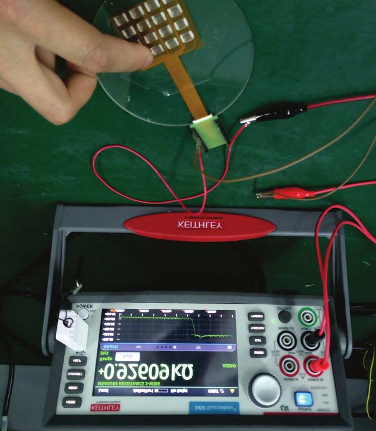
The design of the lower substrate is presented in Figure 3. The area of the G/PET films is
5 mm × 5 mm, and the width of the electrodes is 1 mm. Therefore, the area of each sensing unit
is 5 mm × 7 mm. This is due to the need for adequate connectivity between the upper and lower
substrates. The distance between each sensing unit is 3 mm.
5mm 1mm 3mm
5mm
3mm
Figure 3. Design of the electronic skin.
2.3. Fabrication Process
The fabrication process of the electron skin is presented in Figure 4. First, the lower substrate
is flexible printed circuit board (FPCB), which was fabricated by the standard MEMS technology
(see Figure 4a): (1) Deposit Cu film by the chemical solution deposition method onto the PI substrate;
(2) Cover the photoresistor onto the substrate; (3) Exposure electrode patterns by a photomask;
(4) Develop the film and corrode the extra Cu film; (5) Remove the photoresistor. Second, the graphene
films were obtained by the CVD method, and transferred to the PET substrate by wetting transfer
technology (see Figure 4b). Then, the G/PET was tailored (using scissors) to get the G/PET sensing
unit. Third, the sensing unit was attached onto the electrodes through a uniform layer of silver paste,
using a brush. The silver paste was solidified in a drying box at 60 ◦ C for 2 h. Fourth, the upper
PDMS bump was fabricated by the casting method. The PDMS base and curing agent, in the ratio
10:1, were stirred for 10 m. The PDMS solution was poured into the steel mold, and the PDMS was
vulcanized for 4 h at 80 ◦ C. Fifth, a uniform layer of adhesive PDMS solution was painted onto the
middle of the PDMS bump and the G/PDMS films. Then, the adhesive PDMS solution was cured at
80 ◦ C for 4 h. In this way, the PDMS bump was attached to the G/PET films, as shown in Figure 4c.
The fabricated electronic skin was 43 mm × 37 mm wide and 1.05 mm thick, and the area of the sensing
unit was 5 mm × 7 mm, as shown in Figure 5.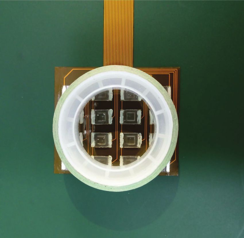
Sensors 2019, 19, 794                                                                                            4 of 11

               Electrode                                   Graphene Film                                   PDMS Bump
                           FPC

                              Transfer graphene                          Attach PDMS bump
                              films to substrate                          to graphene films
           ((a))                                        (b)                                           (c)
                                                                                                      ( )
      Figure 4. The lower substrate was flexible printed circuit (FPCB) fabricated by MEMS technology (a);
      The graphene films were obtained by CVD method and transfered to the substrate (b); The PDMS
      bump was attched to graphene films (c).

                        (a)                                   (b)

                   Figure 5. The size of the electonic skins (a); Photograph of the electronic skin (b).

2.4. Circuit Model
     Our electronic skin is comprised of 16 sensing units, which can be regarded as rheostats.
The resistance of the sensing unit can be changed by applying external pressure. The contact resistance
between the G/PET and the electrodes is lower than the resistance of the G/PET. Therefore, the circuit
model of the electronic skin can be simplified, as shown in Figure 6.

                                      Figure 6. Circuit model of the electronic skin.

2.5. Measurement Model
     When pressure is applied to the surface of the electronic skin, the resistance output of the skin
will change, due to the cracks in the G/PDMS films. According to this principle, we can establish a
measurement model to measure the pressure. The electronic skin contains 16 sensing units which have
two measurement ranges: 0–4 kPa (the small pressure range), and 4–500 kPa (the large pressure range).
                                                                        (R −R )
We use the electronic resistance variation ratios ∆R (∆R = 0R0 p , where R0 and R p correspond to
the resistance without and with pressure, respectively) as the output of the sensing units. Each of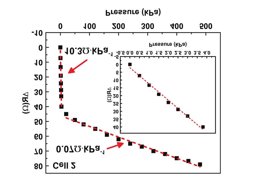
Sensors 2019, 19, 794                                                                                             5 of 11

the ranges of the unit are in a positive linear relationship. Therefore, the measurement model of the
sensing unit can be defined as
                                                              (
                                                                   ap,             p ∈ [0, 4]
                                        ∆R( p) =                                                                     (1)
                                                                  cp + d,        p ∈ [4, 500],

where a, b, c, and d are the sensitivities, and the original output is in the ranges of 0–4 kPa and
4–500 kPa, respectively. Therefore, the measurement model of the electronic skin can be given by
                                        (
                                             aij p + bij ,            p ∈ [0, 4]
                        ∆Rij ( p) =                                                        i, j = (1, 2, 3, 4).      (2)
                                            cij p + dij ,            p ∈ [4, 500]

     In the initial state, the output of the sensing unit is zero; that is, bij = 0. Therefore, Equation (2)
can be written                    (
                                      aij p,       p ∈ [0, 4]
                      ∆Rij ( p) =                                    i, j = (1, 2, 3, 4).                (3)
                                    cij p + dij , p ∈ [4, 500]

3. Experiment
     To carry out the experiment, a home-made pressure measurement platform was constructed,
as shown in Figure 7. The platform was comprised of a digital high-precision stress gauge (F1128
ZQ-20A-2, ZHIQU Precision Instruments Co., Hangzhou, China) and a three-dimensional moving
platform (LZ 60, Hongjinjie Co., Suzhou, China). The measurement range of the digital high-precision
stress gauge is 0–5 N, with an accuracy of 0.001 N. The moving range of the digital high-precision
stress gauge in the vertical direction can reach 10 mm with an accuracy of 0.02 mm. The electronic skin
was measured by a source meter (Keithley 2450, Tektronix Co., Solon, OH, USA).

                                                                  Stress gauge
                             PEAK
                           SET   ZERO
                             ON/OFF

                                                                   Sensing unit
                            0.000 N
                                                                    Source meter

                                                   KEITHLEY

                                              ON/OFF

                                        Three-dimensional moving platform

                           Figure 7. Schematic view and photograph of the experiment.

4. Results and Discussion

4.1. Measurement Model
     According to previous work, we can obtain the measurement model by determining aij , cij ,
and dij (i, j = 1, 2, 3, 4). Therefore, we measured the output of 3 units ((1, 1), (1, 3), (4, 4)), as shown in
Figure 8.
     We can obtain a11 , c11 , and d11 by using the least-squares residual method. With the values
obtained, we get                             (
                                                  8.8p,       p ∈ [0, 4]
                                 ∆R11 ( p) =                                                                (4)
                                               0.07p + 35.2,   p ∈ [4, 500].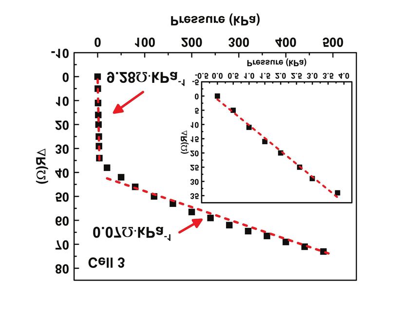
Sensors 2019, 19, 794                                                                                 6 of 11

      Similarly, the measurement model of the sensing unit of the positon (1, 3) can be written
                                               (
                                                      9.28p,        p ∈ [0, 4]
                                 ∆R13 ( p) =                                                             (5)
                                                   0.072p + 37.1,   p ∈ [4, 500],

and the measurement model of the sensing unit of (4, 4) can be written
                                               (
                                                      10.3p,        p ∈ [0, 4]
                                 ∆R44 ( p) =                                                             (6)
                                                   0.07p + 41.2,    p ∈ [4, 500].

     The measurement model of other sensing units of the electronic skin can be measured by the same
method. The electronic skin has the ability to measure not only small pressures (4 kPa).

               (a)                                           (b)
                        Cell 1           Cell 2

                                                   Cell 3

               (c)                                           (d)

      Figure 8. (a) Schematic diagram of the location of the sensing unit; (b–d) Pressure resistance
      characteristic curves of the sensing units.

4.2. Sensitivity
    Sensitivity is the ratio of the resistance variation ratio (∆R) to the corresponding variation of the
applied pressure (F) when the sensor is at a steady state. It is given by

                                                             ∆R
                                                        S=      .                                        (7)
                                                              F
     By substituting experimental data into the above equation, we obtain that the sensitivity of the
sensing unit of the position (1, 1) is 8.8 Ω/kPa in the range of 0–4 kPa, and 0.07 Ω/kPa in the range of
4–500 kPa. Similarly, the sensitivities of the sensing unit of the position (1, 3) and (4, 4) are 9.28 Ω/kPa
and 10.3 Ω/kPa in the range of 0–4 kPa, 0.072 Ω/kPa and 0.07 Ω/kPa in the range of 4–500 kPa.
     The piezoresistive curve showed two segments. The first one is from 0 kPa to 4 kPa,
which corresponds to relatively small pressures. A small pressure deforms the PDMS bump,
which presses the graphene film and generates many small cracks on the graphene film. Because of
the low Young’s modulus of PDMS, a large deformation can be generated by small stress. As a result,
the resistance of the sensor in the first segment increased obviously. The second segment is from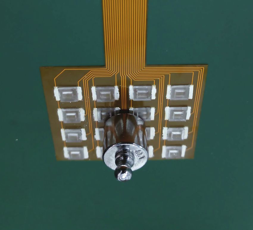
Sensors 2019, 19, 794                                                                                                                7 of 11

4 kPa to 500 kPa, which corresponds to relatively large pressures. In this segment, the deformation of
PDMS bump was saturated. However, with the increased pressure, the PET substrate was deformed,
generating more small cracks on the graphene film. Due to the high Young’s modulus of PET, a larger
pressure is needed to deform the PET, which leads to a reduction in sensitivity. These are shown in
Figure 9.

                                      Without Pressure                         Small Pressure                Large Pressure
                                      Y       X   PDMS        Graphene     Y   X                    Y    X
                        Cross-Section

                                      Z           PET                      Z                        Z
                            View

                                  Z       X                                Z   X
                                                                                                     Z   X
                                  Y                                        Y                         Y
                           Top View

                                                                                                Cracks

                                                         Figure 9. Mechanism of the electronic skin.

4.3. Dynamic Characteristic
       As the electronic skin has potential applications in intelligent robot hands and wearable devices,
it is important to measure the dynamic characteristics of the electronic skin. We used the source meter
to test the dynamic characteristics of the electronic skin. The sampling time of the source meter is
10 ms. The dynamic characteristic was measured with a gentle touch, as shown in Figure 10a.

                                                                                                             20ms             30ms

                                                        (a)                                                          (b)

                                                   20ms             30ms                                      10ms     20ms

                                                        (c)                                                          (d)

      Figure 10. (a) Photograph of the measurement of the dynamic characteristic; (b–d) Measurement
      results of the sensing units.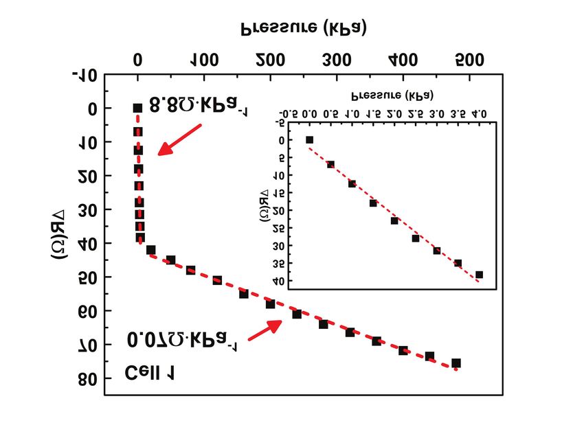
Sensors 2019, 19, 794                                                                                           8 of 11

     Figure 10b–d present the dynamic characteristics of the electronic skin. The loading and unloading
time of the sensing unit at the position (1, 1) were 20 ms and 30 ms, respectively. The measurement
results of the sensing unit at the positions (1, 3) and (4, 4) are shown in Figure 10c,d. We found that
the unloading time was larger than the loading time. This is due to the viscoelastic response of the
PDMS, which required more time to recover its original shape.

4.4. Consistency
     The results in the previous chapter indicated that the outputs of each of the sensing units were not
completely consistent. We can find that the inconsistency of the outputs of the sensing units were larger
in the range of 0–4 kPa. The differences in the dynamic characteristics are not consistent in the range of
0–4 kPa. To explain this result, the graphene film was investigated at different magnifications, by use
of scanning electron microscopy (SEM). We believe that there are two reasons for the inconsistencies:
First, the graphene films may be damaged during the transformation process (from Cu film to PET).
There are many cracks on the graphene film, as shown in Figure 11a. Second, the graphene films may
be ruptured during the tearing process, as shown in Figure 11b. We believe that these reasons lead to
the inconsistency of the sensing units.

                                                                                              500μm

                                      (a)                                      (b)
                        Figure 11. (a) SEM micrograph; and (b) photograph of the graphene film.

4.5. Application
     Our electronic skin has the ability to measure not only the pressure, but also the distribution of
the pressure. We used a blade (0.885 g), a roll of tape (3.958 g), and a weight (10 g) to test the electronic
skin, as shown in Figure 12a–c, respectively.
     The results show that the electronic skin could reproduce the appearance of the objects and
measure the weight of the objects.

4.6. Comparison
    Table 1 shows the comparison between the performances of this work and of others. Generally
speaking, our electronic skin has high-pressure sensitivity, fast response time, and a large
measurement range.

                        Table 1. Comparison between the performances of this work and others.

                                                     Sensitivity   Measurement       Response          Spatial
     Reference          Principle       Material
                                                      (kPa−1 )     Range (kPa)       Times (ms)       Resolution
     This Work      Piezoresistive      G/PET           0.04       0 kPa–500 kPa        20              5 mm
        [21]         Transisitor        G/PET            0.12       0 kPa–40 kPa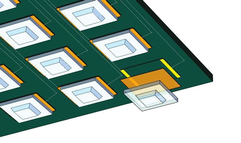
Sensors 2019, 19, 794                                                                                      9 of 11

                        (a)

                        (b)

                        (c)

      Figure 12. The mapping profile of the pixel signals generated by (a) a blade; (b) a roll of tape;
      and (c) a weight.

5. Conclusions
      In this paper, we presented an electronic skin which contains 4 × 4 sensing units, based on
graphene film. Each sensing unit was comprised of PI substrate, graphene film, and a PDMS bump.
The dimensions of the sensing unit were 5 mm × 7 mm × 1 mm. The area of the electronic skin was
43 mm × 37 mm. The working mechanism of the electronic skin was analyzed, and the measurement
model was established. Using this model, the electronic skin was capable of measuring the normal
stress in a range of 0–500 kPa, and of reproducing the appearance of objects. The response time of the
electronic skin was 10 ms. By utilizing the piezoresistive effect of the graphene film, our electronic skin
had high-pressure sensitivity and a fast response time, and has potential application in the fields of
artificial intelligence, robotics, wearable electronics, and prosthetics.

Author Contributions: Conceptualization, X.L. and L.Q.; Methodology, L.Q.; Validation, L.Q. and J.Y.; Formal
Analysis, L.Q.; Writing-Original Draft Preparation, L.Q.; Writing-Review & Editing, J.Y.; Supervision, W.B., X.L.,
L.Z. and R.C.
Funding: The authors thank the financial support from the Science and Technology on Space Physics Laboratory,
the National Natural Science Foundation of China (Grant Nos. 61601342 and 51772030), the Natural Science
Basic Research Plan in Shaanxi Province of China (Program No. 2016ZDJC-07), Shaanxi Postdoctoral Science
Foundation funded project (Grant No. 2017BSHYDZZ36) and the National Key Research and Development
Program of China (2016YFB0100204).
Conflicts of Interest: The authors declare no conflict of interest.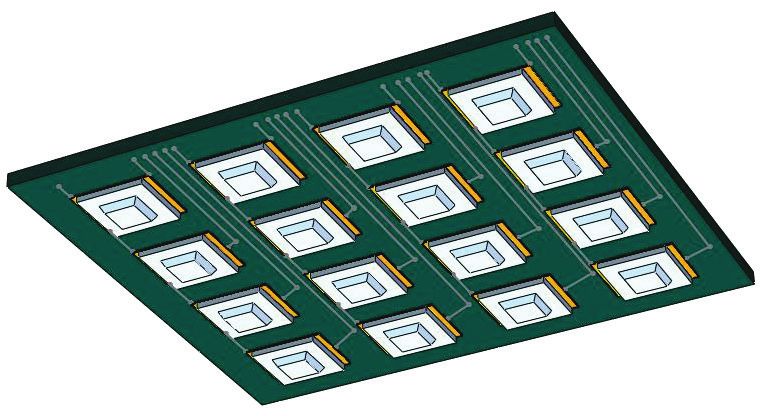
Sensors 2019, 19, 794                                                                                               10 of 11

References
1.    Hammock, M.L.; Chortos, A.; Tee, B.C.K.; Tok, J.B.H.; Bao, Z.N. 25th Anniversary Article: The Evolution of
      Electronic Skin (E-Skin): A Brief History, Design Considerations, and Recent Progress. Adv. Mater. 2013, 25,
      5997–6037. [CrossRef] [PubMed]
2.    Wang, X.W.; Liu, Z.; Zhang, T. AFlexible Sensing Electronics for Wearable/Attachable Health Monitoring.
      Small 2017, 13, 1602790. [CrossRef] [PubMed]
3.    Tan, Y.J.; Wu, J.K.; Li, H.Y.; Tee, B.C.K. Self-Healing Electronic Materials for a Smart and Sustainable Future.
      ACS Appl. Mater. Interfaces 2018, 10, 15331–15345. [CrossRef] [PubMed]
4.    Yang, J.Y.; Ye, Y.S.; Li, X.P.; Lü, X.Z.; Chen, R.J. Flexible, conductive, and highly pressure-sensitive
      graphene-polyimide foam for pressure sensor application. Compos. Sci. Technol. 2018, 164, 187–194.
      [CrossRef]
5.    Chi, C.; Sun, X.G.; Xue, N.; Li, T.; Liu, C. Recent Progress in Technologies for Tactile Sensors. Sensors 2018,
      18, 948. [CrossRef] [PubMed]
6.    Lee, Y.; Park, J.; Cho, S.; Shin, Y.; Lee, H.; Kim, J.; Myoung, J.; Cho, S.; Kang, S.; Baig, C.; et al. Flexible
      Ferroelectric Sensors with Ultrahigh Pressure Sensitivity and Linear Response over Exceptionally Broad
      Pressure Range. ACS Nano 2018, 12, 689–798. [CrossRef] [PubMed]
7.    Jin, M.; Park, S.; Lee, Y.; Lee, J.; Chung, J.; Kim, J.; Kim, J.; Kim, S.; Jee, E.; Kim, D.; et al. An Ultrasensitive,
      Visco-Poroelastic Artificial Mechanotransducer Skin Inspired by Piezo2 Protein in Mammalian Merkel Cells.
      Adv. Mater. 2017, 29, 1605973. [CrossRef] [PubMed]
8.    Kang, S.; Lee, J.; Lee, S.; Kim, S.; Kim, J.; Algadi, H.; Sayari, S.; Kim, D.; Kim, D.; Lee, T. Highly Sensitive
      Pressure Sensor Based on Bioinspired Porous Structure for Real-Time Tactile Sensing. Adv. Electron. Mater.
      2016, 2, 1600356. [CrossRef]
9.    Ha, M.J.; Lim, S.D.; Ko, H.H. Wearable and flexible sensors for user-interactive health-monitoring devices.
      J. Mater. Chem. B 2018, 6, 4043–4064. [CrossRef]
10.   Zang, Y.P.; Zhang, F.J.; Di, C.A.; Zhu, D.B. Advances of flexible pressure sensors toward artificial intelligence
      and health care applications. Mater. Horiz. 2015, 2, 140–156. [CrossRef]
11.   Yang, J.Y.; Li, X.P.; Lü, X.Z.; Chen, W.M.B.R.J. Three-Dimensional Interfacial Stress Sensor Based on Graphene
      Foam. IEEE Sens. J. 2018, 18, 7956–7963. [CrossRef]
12.   Lü, X.Z.; Bao, W.M.; Tao, Y.B.; Yang, J.Y.; Jiang, L.; Jiang, J.N.; Li, X.P.; Xie, K.; Chen, R.J. Three-Dimensional
      Interfacial Stress Decoupling Method for Rehabilitation Therapy Robot. IEEE Trans. Ind. Electron. 2017, 64,
      3970–3977. [CrossRef]
13.   Gao, W.; Emaminejad, S.; Nyein, H.Y.Y.; Challa, S.; Chen, K.; Peck, A.; Fahad, H.M.; Ota, H.; Shiraki, H.;
      Kiriya, D.; et al. Fully integrated wearable sensor arrays for multiplexed in situ perspiration analysis. Nature
      2016, 529, 509–514. [CrossRef] [PubMed]
14.   Minev, I.R.; Musienko, P.; Hirsch, A.; Barraud, Q.; Wenger, N.; Moraud, E.M.; Gandar, J.; Capogrosso, M.;
      Milekovic, T.; Asboth, L.; et al. Electronic dura mater for long-term multimodal neural interfaces. Science
      2015, 347, 159–163. [CrossRef] [PubMed]
15.   Chortos, A.; Liu, J.; Bao, Z.N. Pursuing prosthetic electronic skin. Nat. Mater. 2016, 15, 937–950. [CrossRef]
16.   Tawil, D.S.; Rye, D.; Velonaki, M. Artificial skin and tactile sensing for socially interactive robots: A review.
      Robot. Auton. Syst. 2015, 63, 230–243. [CrossRef]
17.   Joo, Y.S.; Yoon, J.Y.; Ha, J.W.; Kim, T.H.; Lee, S.W.; Lee, B.M.; Pang, C.Y.; Hong, Y.T. Highly Sensitive and
      Bendable Capacitive Pressure Sensor and Its Application to 1 V Operation Pressure-Sensitive Transistor.
      Adv. Electron. Mater. 2017, 3, 1600455. [CrossRef]
18.   Lipomi, D.J.; Cosgueritchian, M.; Tee, B.C.K.; Hellstrom, S.L.; Lee, J.A.; Fox, C.H.; Bao, Z.N. Skin-like
      pressure and strain sensors based on transparent elastic films of carbon nanotubes. Nat. Nanotechnol. 2011, 6,
      788–792. [CrossRef]
19.   Yu, G.H.; Hu, J.D.; Tan, J.P.; Gao, Y.; Lu, Y.F.; Xuan, F.Z. A wearable pressure sensor based on
      ultra-violet/ozone microstructured carbon nanotube/polydimethylsiloxane arrays for electronic skins.
      Nanotechnology 2018, 29, 115502. [CrossRef]
20.   Gong, S.; Schwalb, W.; Wang, Y.W.; Chen, Y.; Tang, Y.; Si, J.; Shirinzadeh, B.J.; Cheng, W.L. A wearable and
      highly sensitive pressure sensor with ultrathin gold nanowires. Nat. Commun. 2014, 5, 3132. [CrossRef]
Sensors 2019, 19, 794 11 of 11
21. Sun, Q.J.; Kim, D.H.; Park, S.S.; Lee, N.Y.; Zhang, Y.; Lee, J.H.; Cho, K.; Cho, J.H. Transparent, Low-Power
Pressure Sensor Matrix Based on Coplanar-Gate Graphene Transistors. Adv. Mater. 2014, 26, 4735–4740.
[CrossRef] [PubMed]
22. Pang, Y.; Tian, H.; Tao, L. Flexible, Highly Sensitive, and Wearable Pressure and Strain Sensors with Graphene
Porous Network Structure. ACS Appl. Mater. Interfaces 2016, 8, 26458–26462. [CrossRef] [PubMed]
23. Jung, J.D.; Lee, D.G.; Park, J.W.; Ko, H.Y.; Lim, H. Piezoresistive Tactile Sensor Discriminating
Multidirectional Forces. Sensors 2015, 15, 25463–25473. [CrossRef] [PubMed]
© 2019 by the authors. Licensee MDPI, Basel, Switzerland. This article is an open access
article distributed under the terms and conditions of the Creative Commons Attribution
(CC BY) license (http://creativecommons.org/licenses/by/4.0/).You can also read