High-Uniformity Planar Mini-Chip-Scale Packaged LEDs with Quantum Dot Converter for White Light Source - Nanoscale Research Letters
←
→
Page content transcription
If your browser does not render page correctly, please read the page content below
Chen et al. Nanoscale Research Letters    (2019) 14:182
https://doi.org/10.1186/s11671-019-2993-z

 NANO EXPRESS                                                                                                                                    Open Access

High-Uniformity Planar Mini-Chip-Scale
Packaged LEDs with Quantum Dot
Converter for White Light Source
Lung-Chien Chen1* , Ching-Ho Tien1, De-Fu Chen2, Zhi-Ting Ye2* and Hao-Chung Kuo3

  Abstract
  This study proposes a novel direct-lit mini-chip-scale packaged light-emitting diode (mini-CSPLED) backlight unit
  (BLU) that used quantum dot (QD) film, diffusion plate, and two prism films to improve brightness uniformity.
  Three different luminous intensity units, 120° mini-CSPLED, 150° mini-CSPLED, and 180° mini-CSPLED with different
  emission angle structures were fabricated using a CSP process. In terms of component characteristics, although the
  180° mini-CSPLED light output power is about loss 4% (at 10 mA) compared with 150° mini-CSPLED, it has a large
  emission angle that forms a planar light source that contributes to improving the BLU brightness uniformity and
  reduced quantity of LEDs at the same area. In terms of BLU analysis, the blue mini-CSPLEDs with different emission
  angles excite the different QD film thicknesses; the chromaticity coordinates conversion to the white light region.
  The BLU brightness increases as the QD film thickness increases from 60, 90, and 150 μm. This result can achieve a
  brightness uniformity of 86% in a 180° mini-CSPLED BLU + 150-μm-thick QD films as compared to the 120° mini-
  CSPLED BLU and 150° mini-CSPLED BLU.
  Keywords: Mini-CSPLED, Quantum dot, GaN, Backlight

Background                                                                             the wide spectrum, the large light decay, and the poor
Liquid crystal display (LCD) is gaining greater favor as                               uniformity of the particles hinder the brightness im-
the mainstream display technology in various contem-                                   provement and CIE chromaticity range of the LCD; thus,
porary society fields. With the improvement of living                                  there is still room for improvement. It is well known
standards, people have higher and higher requirements                                  that white LEDs are mainly fabricated by coating a YAG
on LCD display quality. Especially in terms of color                                   yellow phosphor layer onto a gallium nitride (GaN) blue
gamut and brightness, LCDs are constantly being sur-                                   LED (wavelength 450–470 nm) [7, 8]. However, its emis-
passed by other display technologies such as organic                                   sion spectrum lacks red light, emits cool white light, is
light-emitting diodes (OLEDs) and laser displays [1–3].                                not natural enough, and has poor color rendering (CRI
In order to improve LCD performance, light-emitting di-                                less than 75), which limits its application in high-end
odes (LEDs) have gradually replaced the traditional cold                               lighting and special fields. In order to obtain high CRI
cathode fluorescent lamp (CCFL) due to its small size,                                 LEDs, a small amount of red phosphor and a small
low energy consumption, and low heat generation. LEDs                                  amount of green phosphor are added to the yellow phos-
have become the new generation of LCD backlight unit                                   phor to compensate and change the spectrum [6, 9].
(BLU) source [4–6]. At present, the LED BLU uses a                                     However, this method of LED coated with phosphor is
blue LED to excite the yellow phosphor to form a white                                 still insufficient in terms of luminous efficiency and
backlight. However, the low efficiency of the phosphor,                                chemical stability, and it is difficult to obtain large-scale
                                                                                       popularization and application.
* Correspondence: ocean@ntut.edu.tw; ztye@nuu.edu.tw                                      As a new type of fluorescent semiconductor nanocrys-
1
 Department of Electro-optical Engineering, National Taipei University of
Technology, No. 1, 3 Sec., Chung-Hsiao E. Rd, Taipei 10608, Taiwan
                                                                                       tals, nano quantum dots (QDs) have many unique op-
2
 Department of Electro-Optical Engineering, National United University, 2,             tical properties, such as high photoluminescence
Lienda, Miaoli 26063, Taiwan                                                           quantum yield, narrow emission spectrum, tunable
Full list of author information is available at the end of the article

                                        © The Author(s). 2019 Open Access This article is distributed under the terms of the Creative Commons Attribution 4.0
                                        International License (http://creativecommons.org/licenses/by/4.0/), which permits unrestricted use, distribution, and
                                        reproduction in any medium, provided you give appropriate credit to the original author(s) and the source, provide a link to
                                        the Creative Commons license, and indicate if changes were made.
Chen et al. Nanoscale Research Letters   (2019) 14:182                                                        Page 2 of 10

emission spectrum, and high color purity [10–16]. It has        Methods
been demonstrated that in the efficient photon manage-          The GaN LED epiwafer with an emission wavelength
ment, QD converter can be widely used in solar cells            of 460 nm was grown by metal–organic chemical
[17, 18], LEDs [19, 20], and photodetectors [21–23]. Es-        vapor deposition (MOCVD) on a c-plane sapphire
pecially, QD photodetectors with selectable wavelengths         substrate. The LED structure consists of a 2-μm-thick
and high responsivity and on/off ratio have been re-            undoped GaN layer, a 2.0-μm-thick Si-doped n-type
ported [24, 25]. Recently, QDs were also applied for            GaN cladding layer, six periods of InGaN/GaN mul-
water splitting due to its superior electrocatalytic and        tiple quantum wells (MQW), a 25-nm-thick Mg-doped
photocatalytic properties [26]. QDs have become a suit-         p-AlGaN electron blocking layer, and a 0.2-μm-thick
able candidate material in the display field, which has         Mg-doped p-type GaN cladding layer. The Ni/Ag/Ni/
great potential to replace the traditional phosphor pow-        Pt layers for ohmic contact layer and reflector were
der and increase the LCD color gamut range [27, 28].            deposited onto the LED via electron beam evaporating
QD-based backlight technology is currently the main-            system. Three different emission angle mini FC-LED
stream application target in displays, which have a great       (mini-LED) structures used in this study were fabri-
deal of attention from both the scientific and industrial       cated by film transfer technique and molded chip scale
circles. QDs are generally composed of groups II–VI or          package (CSP) method, with a detailed comparison:
III–V elements and have a crystal grain diameter of only        120° mini-CSPLED, 150°mini-CSPLED, and 180°mini-
about 2–10 nm [29, 30]. Due to the quantum confine-             CSPLED, as shown in Fig. 1. The 120° mini-CSPLED
ment effect, the QD energy gap can change with the              structure has a protective layer on all four sides of the
particle size. In the past few years, research on cad-          chip and a transparent layer on the light emission sur-
mium selenide (CdSe) and its core-shell QDs in dis-             face. The 150° mini-CSPLED structure has a transpar-
play technology has been the most popular, mainly               ent layer on the side and the light emission surface of
because its light emission wavelength falls within the          the chip. The 180° mini-CSPLED structure has a
visible range. The QD-LED device structure is similar           transparent layer on the side and the light emission on
to that of a polymer light-emitting diode (PLED), and           the chip surface, with a diffusion reflective layer cov-
its emission layer is spin-coated using a colloidal             ered onto the topmost layer. Where the material
semiconductor QDs solution, thereby having the ad-              source of the transparent layer is the TiO2/silicone
vantages of the simple preparation process, low cost,           resin nanocomposite, both the thick protective layer
and flexibility for fabrication [31–33].                        and the thin diffusion reflective layer are the TiO2
   At present, the mainstream LED BLU light source ar-          powders. QD films were fabricated using CdSe/ZnS
rangement can be roughly divided into two types: edge-lit       core-shell QDs as the material source. The green-
and direct-lit. In general, the contrast and brightness uni-    emission (~ 525 nm) and red-emission (~ 617 nm)
formity provided by the direct-lit will be better than the      CdSe/ZnS core-shell QDs were mixed with poly-
edge-lit. Edge-lit brightness uniformity uses a light guide     methylmethacrylate (PMMA) to prepare various QD
plate to distribute light across the entire screen. However,    film thicknesses, in which the QD film optical charac-
the light guide plate weight becomes too great for large        teristics can be found in Additional file 1: Figure S1.
size LCD-TV applications. In addition, it needs to have         These QD films were fabricated as a color converter
good optical quality, resulting in high cost. Direct-lit does   onto a LED chip (λ = 450 nm) to obtain white light de-
not use a light guide; the LED array is evenly placed dir-      vices. Figure 2 displays the BLU structure (18 mm ×
ectly below the LCD panel, which provides outstanding           18 mm), which consists of 3 × 3 square-shaped
performance in brightness uniformity and good optical ef-       mini-LED array, diffusion plate, QD films, and two
ficiency [34–36]. The BLU brightness and uniformity has         prism films. The mini-LED array was mounted onto a
a great influence on the display module uniformity. There-      circuit board with a chip size of 20 mil ×20 mil and a
fore, it is very important to improve the BLU brightness        pitch length of 5.1 mm. The effective optical distance
uniformity. However, in actual applications, the BLU illu-      (OD), by considering between chip and diffusion plate,
mination uniformity is difficult to maintain. The bright-       is set as 2.5 mm in order to obtain good spatial uni-
ness non-uniformity will be significantly different when        formity. Figure 3 shows a blue mini LED array to ex-
the module becomes thinner. In order to achieve a thin          cite QD films of different thicknesses (for instance,
LED and good uniformity, it is more challenging to design       60-μm-, 90-μm-, and 150-μm-thick QD films) to ob-
a BLU that meets the requirement. This study proposes a         tain a white planar light source. The brightness uni-
method to improve the LED BLU brightness uniformity.            formity of the entire panel is evaluated as shown in
The BLU brightness uniformity was discussed through the         Fig. 3 by measuring brightness in five points, L1–L5,
different LED emission angles and the different QD film         located on the panel. The BLU brightness uniformity
thicknesses.                                                    in this study is expressed by the following formula:
Chen et al. Nanoscale Research Letters     (2019) 14:182                                                                           Page 3 of 10

               LED chip                    transparent layer                        protective layer                      reflective layer

                   LED                                             LED                                              LED

     (a) 120°-mini-CSPLED                              (b) 150°-mini-CSPLED                            (c) 180°-mini-CSPLED
 Fig. 1 Schematic diagrams of three kinds of mini-CSPLED emission angle structure. a 120° mini-CSPLED, b 150° mini-CSPLED, and c
 180° mini-CSPLED

                                   L1 þ L2 þ L3 þ L4 þ L5                is clear that the I–V curves of these three devices are al-
    Brightness uniformity ¼                                              most identical, demonstrating that the CSP process does
                                             5
                                                                 ð1Þ     not damage the electrical properties. On the other hand,
                                                                         the L–I curve shows only a slight difference in the light
                                                                         output power of the 120° mini-CSPLED, 150°
  The light output power–current–voltage (L–I–V) char-                   mini-CSPLED, and 180° mini-CSPLED, which indicates
acteristics of these mini-CSPLED was measured at room                    the result of successful device optimization via the CSP
temperature using a Keithley 2400 source meter and an                    structure. On the other hand, the light output power of
integrated sphere with a calibrated power meter (CAS                     the three kinds of mini-CSPLEDs initially increases
140B, Instrument Systems, Munich). The spatial radiation                 linearly with the injection current. The L–I curve shows
patterns of these mini-CSPLEDs were measured using a                     only a slight difference in the light output power of the
goniophotometer (LEDGON-100, Instrument Systems,                         120° mini-CSPLED, 150° mini-CSPLED, and 180°
Munich). The BLU luminance and electroluminescence                       mini-CSPLED, which indicates the result of successful de-
(EL) spectra with QD films were analyzed using a spectral                vice optimization via the CSP structure. As the injection
luminance meter (SRI-RL-5000, Optimum Optoelectron-                      current increased up to 200 mA, the light output power of
ics Corp., Taiwan).                                                      the three kinds of mini-CSPLEDs were approximately
                                                                         250.9, 258.0, and 245.9 mW. The light output power of
Results and Discussion                                                   the 120° mini-CSPLED exhibits lower than 150°
Figure 4 presents the measured L–I–V characteristics for                 mini-CSPLED, which may be absorbed by the diffusion re-
the three kinds of mini-CSPLED. At an injection current                  flective layer. The 180° mini-CSPLED gives 2.05% and
of 20 mA, the forward voltages of the 120° mini-CSPLED,                  4.93% deterioration in the light output power at a high
150° mini-CSPLED, and 180° mini-CSPLED were all the                      current of 200 mA as compared to the 120° mini-CSPLED
same and ∼ 2.72 V. Further increasing the injection                      and 150° mini-CSPLED. The deterioration could be attrib-
current to 200 mA, the forward voltages of these three                   uted to the addition of a diffusion reflective layer on top
types mini-CSPLED were all increased to 3.09–3.14 V. It                  of the transparent layer/CSPLED, the light may be slightly

 Fig. 2 Schematic diagrams of the backlight unit structure
Chen et al. Nanoscale Research Letters (2019) 14:182 Page 4 of 10
18 mm
L2 L3
L1 18 mm
L4 L5
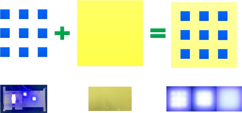
Blue mini-CSPLED QD film
120°\150°\180° 150 µm Measuring Position
@120° @150° @180°
QD film
150 µm
Fig. 3 Schematic diagrams of the brightness uniformity measurement
absorbed, or most of the light is concentrated in the be found that the central light output intensity of the ra-
transparent layer, with the reflection emitted from the diation pattern of the 180° mini-CSPLED was depressed
sidewall. to half due to the diffusion reflective layer on the top.
Figure 5 shows the radiation patterns of the 120° The wider viewing angle was caused by much light es-
mini-CSPLED, 150° mini-CSPLED, and 180° mini- cape from the transparent layer after being reflected by
CSPLED at an injection current of 100 mA. The radi- the diffusion reflective layer, i.e., emission pattern with a
ation pattern of mini-CSPLEDs can be controlled by butterfly wing-shaped light distribution; thus, it can be
varying the package structures. The 120° mini-CSPLED, used as a planar light source. On the other hand, the
150° mini-CSPLED, and 180° mini-CSPLED viewing an- 120° mini-CSPLED was covered with a diffusion reflect-
gles were measured to be 110.6°, 148.7°, and 180°, re- ive layer on all four sides, so that the light was concen-
spectively. Obviously, the viewing angle of the 180° trated and emitted upwards to form a Lambertian
mini-CSPLED radiation pattern was larger than that of shaped light distribution. In addition, due to the
the 120° mini-CSPLED and 150° mini-CSPLED. It can five-sided conformal covered with a transparent layer,
Fig. 4 The L–I–V characteristics of the 120° mini-CSPLED, 150° mini-CSPLED, and 180° mini-CSPLED
Chen et al. Nanoscale Research Letters (2019) 14:182 Page 5 of 10
Fig. 5 Radiation patterns of the 120° mini-CSPLED, 150° mini-CSPLED, and 180° mini-CSPLED (at 10 mA)
the light distribution of the 150° mini-CSPLED was simi- − 0.2295), and (x, y) = (x = 0.1947 − 0.2496, y = 0.1328 −
lar to the batwing-shaped light distribution. 0.2331), respectively. It was clear that the emission chro-
Table 1 shows the optoelectronic properties of the maticity coordinates of the corresponding BLU with QD
mini-CSPLED blue BLUs with different emission angles. films of various thicknesses exhibiting CIE chromaticity
With the same forward voltage of 24 V (at 10 mA), the coordinates were located near the blue region. As the QD
CIE chromaticity coordinates (x, y) of the 120° film thickness increases, the CIE chromaticity coordinates
mini-CSPLED BLU, the 150° mini-CSPLED BLU, and shift toward the white region. In addition, the BLU bright-
the 180° mini-CSPLED BLU were all similar and (x, y) = ness increases as the QD film thickness increases from 60,
(x = 0.1518 − 0.15.2, y = 0.026 − 0.0281). Furthermore, 90, and 150 μm. This result was attributed to the signifi-
the light output powers of the 120° mini-CSPLED blue cant increases the excitation probability with thick QD
BLU, 150° mini-CSPLED blue BLU, and 180° films to produce white light and increase brightness. On
mini-CSPLED blue BLU were measured at 147.43, the other hand, the BLU brightness of the 180°
153.02, and 146.71 mW, respectively. Due to the 180° mini-CSPLED BLU was significantly lowered, which may
mini-CSPLED package structure factor, the light output be attributed to the average brightness decrease as a result
power was slightly poor, but the illumination area was of the larger illumination area. The results of this study
increased. show the CIE chromaticity coordinates (x, y) and bright-
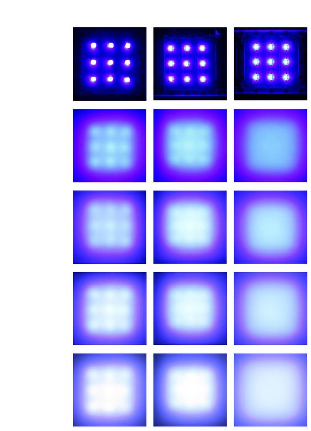
Figures 6a–c show the CIE chromaticity diagram of 120° ness for the three kinds of mini-CSPLED emission angle
mini-CSPLED BLU, 150° mini-CSPLED BLU, and 180° structure with different QD film thicknesses and are sum-
mini-CSPLED BLU with different QD film thicknesses. marized in Tables 2, 3, and 4, in which the data measure-
The CIE chromaticity coordinates (x, y) of the three kinds ment can be found in Additional file 1: Figures S2–S10.
of mini-CSPLED BLUs with different QD film thicknesses Figures 7a–e show the light distribution images of
were measured as follows:(x, y) = (x = 0.1977 − 0.2525, y = 120° mini-CSPLED BLU, 150° mini-CSPLED BLU, and
0.1297 − 0.2284), (x, y) = (x = 0.1941 − 0.2478, y = 0.1239 180° mini-CSPLED BLU with and without a diffusor and
different QD film thicknesses. Figure 7a shows the light
distribution images of the three kinds of mini-CSPLED
Table 1 Optoelectronic properties of the three kinds of mini
LED blue BLU
blue BLUs without diffusor and QD films. By placing the
diffusion plate on the three kinds of mini-CSPLED
120o 150o 180o
BLUs, it can be seen that the 180° mini-CSPLED BLU
Chip size 20 mil × 20 mil
has a better uniform planar light compared to the 120°
Package size 1 mm × 1 mm mini-CSPLED BLU and 150° mini-CSPLED BLU. How-
Vf (V) 24 24 24 ever, the 120° mini-CSPLED BLU and the 150°
If (mA) 10 10 10 mini-CSPLED BLU show the stripe patterns, in which
x 0.1518 0.1507 0.1502 the 120° mini-CSPLED BLU is the most visible, as
y 0.026 0.0276 0.0281
shown in Fig. 4b. Similarly, as shown in Figs. 7c–e, the
QD films are placed on the diffusion plate, and as the
Light output power (mW) 147.43 153.02 146.71
QD film thickness is increased, the light distribution
Chen et al. Nanoscale Research Letters       (2019) 14:182                                                                           Page 6 of 10

    Fig. 6 CIE chromaticity diagrams of 120° mini-CSPLED BLU, 150° mini-CSPLED BLU, and 180° mini-CSPLED BLU with different QD film thickness

Table 2 The CIE chromaticity coordinates (x, y) and brightness              Table 3 The CIE chromaticity coordinates (x, y) and brightness
for the 120°mini-CSPLEDs with different QD film thicknesses                 for the 150° mini-CSPLEDs with different QD film thicknesses
120° mini-CSPLED                                                            150° mini-CSPLED
QD film thickness (μm)            60             90              150        QD film thickness (μm)          60              90              150
x                                 0.1977         0.2162          0.2525     x                               0.1941          0.2121          0.2478
y                                 0.1297         0.1683          0.2284     y                               0.1239          0.1707          0.2295
Brightness (cd/m2)                8,532          9,561           9,900      Brightness (cd/m2)              9,638           11,331          10,319
Chen et al. Nanoscale Research Letters (2019) 14:182 Page 7 of 10
Table 4 The CIE chromaticity coordinates (x, y) and brightness region using 150-μm-thick QD films. Therefore, the
for the 180° mini-CSPLEDs with different QD film thicknesses thickness of QD films was fixed, and the effects of
180° mini-CSPLED brightness uniformity of the three kinds of
QD film thickness (μm) 60 90 150 mini-CSPLED BLUs were discussed. Using the 5-point
x 0.1947 0.2137 0.2496 brightness uniformity measurement method, the bright-
ness uniformity of the three kinds of mini-CSPLED BLU
y 0.1328 0.1725 0.2331
+ 150-μm-thick QD films were estimated to be 35%,
Brightness (cd/m2) 7,365 8,463 8,645
39%, and 86%, respectively. Obviously, there were 1.47
times and 1.19 times improvement in the BLU bright-
images of the three kinds of mini-CSPLED BLUs clearly ness uniformity of 180° mini-CSPLED BLU compared
presented that the BLU brightness is increased and is with that of the 120° mini-CSPLED BLU and 150°
closer to white light; the stripe pattern is also less and mini-CSPLED BLU. Therefore, it was found that the use
less unobvious. The light distribution images observa- of 180° mini-CSPLED BLU +150-μm-thick QD film
tions are in good agreement with the CIE chromaticity could effectively improve the overall BLU brightness
coordinates (x, y) and brightness results. uniformity. The brightness uniformity calculation of the
From the above results, it can be seen that the CIE three kinds of mini-CSPLED BLUs + 150-μm-thick QD
color coordinates (x, y) can be brought close to the white films was summarized in Table 5, in which the data
120°-mini-CSPLED 150°-mini-CSPLED 180°-mini-CSPLED
(a)
(b)
(Without QD films)
(c)
+ 60 µm QD film
(d)
+ 90 µm QD film
(e)
+ 150 µm QD film
Fig. 7 Light distribution images of 120° mini-CSPLED BLU, 150° mini-CSPLED BLU, and 180° mini-CSPLED BLU with and without a diffusion plate
and different QD film thicknessChen et al. Nanoscale Research Letters (2019) 14:182 Page 8 of 10
Table 5 Brightness uniformities of three kinds of mini-CSPLED to (0.2794, 0.3063). This shows that with the addition of
BLUs with 150-μm-thick QD films LCD, the CIE chromaticity coordinates shifted more to-
Mini-CSPLED type 120° 150° 180° ward the white region. The EL spectrum of the three
2
L1 (center) (cd/m ) 9,900 10,319 8,645 kinds of mini-CSPLED BLUs + 150-μm-thick QD films
L2 (cd/m2) 1,803 2,557 7,110 without LCD exhibits a strong blue light intensity, and
2 the CIE chromaticity coordinate is located in the near
L3 (cd/m ) 1,393 2,385 7,227
blue region, as shown in Fig. 8b (see Additional file 1:
L4 (cd/m2) 2,368 2,405 7,226
Figures S4, S7, and S10). When the LCD was placed on
2
L5 (cd/m ) 1,783 2,652 7,050 the three kinds of mini-CSPLED BLUs + 150 μm-thick
L1 (center) (%) 100% 100% 100% QD films, the EL spectrum shows that the red, green,
L2 (%) 18% 25% 82% and blue light intensity were similar, and the CIE chro-
L3 (%) 14% 23% 84% maticity coordinate was located in the white region. This
result can be attributed to the color filter of the LCD
L4 (%) 24% 23% 84%
structure, which improves the color coordinate position,
L5 (%) 18% 26% 82%
as shown in Fig. 8c (see Additional file 1: Figures S23–
Brightness uniformity (%) 35% 39% 86% S25). The inset shows the actual application photograph
of 180° mini-CSPLED BLU + 150-μm-thick QD film
measurement can be found in Additional file 1: Figures with LCD.
S11–S22.
Figures 8a–c show the CIE chromaticity diagram and Conclusions
EL spectra of the three kinds of mini-CSPLED BLUs + In conclusion, we successfully used mini-CSPLED BLU as
150 μm-thick QD films with and without LCD. As the blue light and excitation energy source, along with QD
shown in Fig. 8a, it can be seen that the CIE chromati- films, to produce a uniform white backlight. Mini-
city coordinate (x, y) of the 120° mini-CSPLED BLU with CSPLEDs were subjected to emission angle packaged
LCD shifted from (0.2525, 0.2284) to (0.2873, 0.3099). structure fabricate for 120°, 150°, and 180° to verify that
The 150° mini-CSPLED BLU with LCD was from the mini-CSPLED optical performance had significant dif-
(0.2478, 0.2295) to (0.2830, 0.3072). The 180° ferences. The lager emission angle and an illumination
mini-CSPLED BLU with LCD was from (0.2496, 0.2331) area of 180° mini-CSPLED improved significantly when
Fig. 8 a CIE chromaticity diagram. b, c EL spectra of three kinds of mini-CSPLED BLUs + 150 μm-thick QD films with and without LCDChen et al. Nanoscale Research Letters (2019) 14:182 Page 9 of 10
compared with that of the 120° mini-CSPLED and 150° Authors’ Contributions
mini-CSPLED. Impressively, 180° mini-CSPLED BLU with LCC carried out the experiments, designed the study, and gave significant
suggestions on the writing for the entire manuscript. CHT conceived the
a 150-μm-thick QD film achieved an excellent uniform original idea and wrote the manuscript. DFC prepared the samples and
brightness planar white light source for backlight displays carried out all the measurements. ZTY and HCK helped to analyze and
of approximately 86%, which is significant for the future interpret the data and helped to draft the manuscript. All authors read and
approved the final manuscript.
ultra-thin display technology. We implemented highly re-
liable CSP technology that can protect the LED chip, solve Ethics Approval and Consent to Participate
the emission angle and illumination area problems of Not applicable.
LEDs, and fabricate a backlight source for displays with
Competing Interests
good brightness uniformity. The authors declare that they have no competing interests.
Additional File Publisher’s Note
Springer Nature remains neutral with regard to jurisdictional claims in published
maps and institutional affiliations.
Additional file 1: Figure S1. QD films characteristics – PL spectrum
(excited by a 405 nm laser). Figure S2. Spectroradiometric report of 120°- Author details
mini-CSPLED with a 60 μm-thick QD films. Figure S3. Spectroradiometric 1
Department of Electro-optical Engineering, National Taipei University of
report of 120°-mini-CSPLED with a 90 μm-thick QD films. Figure S4. Technology, No. 1, 3 Sec., Chung-Hsiao E. Rd, Taipei 10608, Taiwan.
Spectroradiometric report of 120°-mini-CSPLED with a 150 μm-thick QD 2
Department of Electro-Optical Engineering, National United University, 2,
films. Figure S5. Spectroradiometric report of 150°-mini-CSPLED with a Lienda, Miaoli 26063, Taiwan. 3Department of Photonics and Institute of
60 μm-thick QD films. Figure S6. Spectroradiometric report of 150°-mini- Electro-Optical Engineering, National Chiao Tung University, Hsinchu 30010,
CSPLED with a 90 μm-thick QD films. Figure S7. Spectroradiometric re- Taiwan.
port of 150°-mini-CSPLED with a 150 μm-thick QD films. Figure S8. Spec-
troradiometric report of 180°-mini-CSPLED with a 60 μm-thick QD films. Received: 6 March 2019 Accepted: 29 April 2019
Figure S9. Spectroradiometric report of 180°-mini-CSPLED with a 90 μm-
thick QD films. Figure S10. Spectroradiometric report of 180°-mini-
CSPLED with a 150 μm-thick QD films. Figure S11. The L2 spectroradio-
References
metric report of 120°-mini-CSPLED with a 150 μm-thick QD films. Figure
1. Chen HW, Tan GJ, Wu ST (2017) Ambient contrast ratio of LCDs and OLED
S12. The L3 spectroradiometric report of 120°-mini-CSPLED with a 150
displays. Opt Express 25(26):33643–33656.
μm-thick QD films. Figure S13. The L4 spectroradiometric report of 120°-
2. Tang CW, Vanslyke SA (1987) Organic electroluminescent diodes. Appl Phys
mini-CSPLED with a 150 μm-thick QD films. Figure S14. The L5 spectrora-
Lett 51(12):913–915.
diometric report of 120°-mini-CSPLED with a 150 μm-thick QD films. Fig-
3. Song H, Li H, Liu X (2018) Studies on different primaries for a nearly-
ure S15. The L2 spectroradiometric report of 150°-mini-CSPLED with a
ultimate gamut in a laser display. Opt Express 26(18):23436–23448.
150 μm-thick QD films. Figure S16. The L3 spectroradiometric report of
4. Lv X, Loo KH, Lai YM, Tse CK (2014) Energy-saving driver design for
150°-mini-CSPLED with a 150 μm-thick QD films. Figure S17. The L4
full-color large-area LED display panel systems. IEEE Trans Ind Electron.
spectroradiometric report of 150°-mini-CSPLED with a 150 μm-thick QD
61(9):4665–4673.
films. Figure S18. The L5 spectroradiometric report of 150°-mini-CSPLED
5. Templier F (2016) GaN-based emissive microdisplays: A very promising
with a 150 μm-thick QD films. Figure S19. The L2 spectroradiometric re-
technology for compact, ultra-high brightness display systems. J Soc Inf
port of 180°-mini-CSPLED with a 150 μm-thick QD films. Figure S20. The
Display 24(11):669–675.
L3 spectroradiometric report of 180°-mini-CSPLED with a 150 μm-thick
6. Wang L, Wang X, Kohsei T, Yoshimura K, Izumi M, Hirosaki N, Xie RJ (2015)
QD films. Figure S21. The L4 spectroradiometric report of 180°-mini-
Highly efficient narrow-band green and red phosphors enabling wider
CSPLED with a 150 μm-thick QD films. Figure S22. The L5 spectroradio-
color-gamut LED backlight for more brilliant displays. Opt Express 23(22):
metric report of 150°-mini-CSPLED with a 150 μm-thick QD films. Figure
28707–28717.
S23. Spectroradiometric report of 120°-mini-CSPLED + 150 μm-thick QD
7. Lin HT, Tien CH, Hsu CP, Horng RH (2014) White thin-film flip-chip LEDs
films with LCD. Figure S24. Spectroradiometric report of 150°-mini-
with uniform color temperature using laser lift-off and conformal phosphor
CSPLED + 150 μm-thick QD films with LCD. Figure S25. Spectroradio-
coating technologies. Opt Express 22(26):31646–31653.
metric report of 180°-mini-CSPLED + 150 μm-thick QD films with LCD.
8. Tien CH, Ho KW, Chien HY, Wuu DS, Horng RH (2016) Effect of the
(DOCX 3461 kb)
phosphor permanent substrate on the angular CCT for white thin-film flip-
chip light-emitting diodes. IEEE Trans Electron Devices 63(10):3977–3982.
9. Yang SH, Lin JS, Juang FS, Chou DC, Chung MH, Chen CM, Liu LC (2013)
Abbreviations White light emitting diodes (LEDs) with good color rendering indices (CRI)
BLU: Backlight unit; CCFL: Cold cathode fluorescent lamp; CdSe: Cadmium and high luminous efficiencies by the encapsulation of mixed and double-
selenide; GaN: Gallium nitride; LCD: Liquid crystal display; mini-CSPLED: Mini deck phosphors. Curr Appl Phys 13(5):931–934.
chip-scale packaged light-emitting-diode; OLED: Organic light-emitting 10. Coe S, Woo W-K, Bawendi M, Bulović V (2002) Electrolumi-nescence from
diode; PLED: Polymer light-emitting diode; QDs: Quantum dots; YAG: Yttrium single monolayers of nanocrystals in molecularorganic devices. Nature
aluminum garnet 420(6917):800–803.
11. Colvin VL, Schlamp MC, Alivisatos AP (1994) Light-emitting diodes made
from cadmium selenide nanocrystals and a semiconducting polymer.
Acknowledgements Nature 370(6488):354–357.
This work was supported by the Ministry of Science and Technology 12. Chen HS, Hsu CK, Hong HY (2006) InGaN-CdSe-ZnSe quantum dots white
(Taiwan) under Contract No. 107-2221-E-027-053. LEDs. IEEE Photonics Technol Lett. 18(1):193–195.
13. Janssen RAJ, Stouwdam JW (2008) Red, green, and blue quantum dot LEDs
with solution processable ZnO nanocrystal electron injection layers. J Mater
Funding Chem. 18(16):1889–1894.
The authors gratefully acknowledge the financial support from the Ministry 14. Al-Amri AM, Cheng B, He J-H (2019) Perovskite methylammonium lead
of Science and Technology of the Republic of China under Contract No. trihalide heterostructures: progress and challenges. IEEE Trans Nano
MOST 107-2221-E-027-053. Technol. 18:1–12.Chen et al. Nanoscale Research Letters (2019) 14:182 Page 10 of 10
15. Cheng B (2019) Orthogonal patterning halide perovskite for nanodevice
application. ACS Nano 13(2):1490–1498.
16. Tseng JY, Lee L, Huang YC, Chang JH, Su TY, Shih YC, Lin HW, Chueh YL
(2018) Pressure welding of silver nanowires networks at room temperature
as transparent electrodes for efficient organic light-emitting diodes. Small
14(38):1800541.
17. Das S, Hossain MJ, Leung SF, Lenox A, Jung Y, Davis K, He JH, Roy T (2019)
A leaf-inspired photon management scheme using optically tuned bilayer
nanoparticles for ultra-thin and highly efficient photovoltaic devices. Nano
Energy 58:47–56.
18. Wang HP, Periyanagounder D, Li AC, He JH (2019) Fabrication of Silicon
Hierarchical Structures for Solar Cell Applications. IEEE Access 7:19395–19400.
19. Chen GH, Yeh CW, Yeh MH, Ho SJ, Chen HS (2015) Wide gamut white light
emitting diodes using quantum dot-silicone film protected by an atomic
layer deposited TiO2 barrier. Chem Commun. 51:14750.
20. Choi MK, Yang J, Hyeon T, Kim DH (2018) Flexible quantum dot
light-emitting diodes for next-generation displays. NPJ Flexible Electron. 2:10.
21. Malinowski PE, Georgitzikis E, Maes J, Vamvaka I, Frazzica F, Olmen JV, Moor
PD, Heremans P, Hens Z, Cheyns D (2017) Thin-film quantum dot
photodiode for monolithic infrared image sensors. Sensors 17(12):2867.
22. Yang W, Chen J, Zhang Y, Zhang Y, He JH, Fang X (2019) Silicon-compatible
photodetectors: trends to monolithically integrate photosensors with chip
technology. Adv Func Mater 1808182.
23. Chen YZ, Wang SW, Su TY, Lee SH, Chen CW, Yang CH, Wang K, Kuo HC,
Chueh YL (2018) Phase-engineered type-II multimetal–selenide
heterostructures toward low-power consumption, flexible, transparent, and
wide-spectrum photoresponse photodetectors. Small 14(22):1704052.
24. Alarawi A, Ramalingam V, He JH (2019) Recent advances in emerging single
atom confined two-dimensional materials for water splitting applications.
Mater Today Energy 11:1–23.
25. Tang SY, Medina H, Yen YT, Chen CW, Yang TY, Wei KH, Chueh YL (2019)
Enhanced photocarrier generation with selectable wavelengths by M-
decorated-CuInS2 nanocrystals (M = Au and Pt) synthesized in a single
surfactant process on MoS2 bilayers. Small 15(8):1803529.
26. Liang X, Dong R, Ho JC (2019) Self-assembly of colloidal spheres toward
fabrication of hierarchical and periodic nanostructures for technological
applications. Adv Mate Tech 4(3):1800541.
27. Kim HJ, Shin MH, Kim YJ (2016) Optical efficiency enhancement in white
organic light-emitting diode display with high color gamut using patterned
quantum dot film and long pass filter. Jpn. J Appl Phys. 55(8S3):08RF01.
28. Chung W, Park K, Yu HJ, Kim J, Chun BH, Kim SH (2010) White emission
using mixtures of CdSe quantum dots and PMMA as a phosphor. Opt Mater
32(4):515–521.
29. Xie R, Kolb U, Li J, Basché T, Mews A (2005) Synthesis and Characterization
of Highly Luminescent CdSe-Core CdS/Zn0.5Cd0.5S/ZnS Multishell
Nanocrystals. J Am Chem Soc 127(20):7480–7488.
30. Baek J, Shen Y, Lignos I, Bawendi MG, Jensen KF (2018) Multistage
microfluidic platform for the continuous synthesis of III–V core/shell
quantum dots. Angew Chem Int Edit 57(34):10915–10918.
31. Chung DY, Huang J, Bradley DDC, Campbell AJ (2010) High performance,
flexible polymer light-emitting diodes (PLEDs) with gravure contact printed
hole injection and light emitting layers. Org Electron 11(6):1088–1095.
32. Zheng H, Zheng Y, Liu N, Ai N, Wang Q, Wu S, Zhou J, Hu D, Yu S, Han S,
Xu W, Luo C, Meng Y, Jiang Z, Chen Y, Li D, Huang F, Wang J, Peng J, Cao Y
(2013) All-solution processed polymer light-emitting diode display. Nat
Commun 4:1971.
33. Niu Q, Shao Y, Xu W, Wang L, Han S, Liu N, Peng J, Cao Y, Wang J (2008)
Full color and monochrome passive-matrix polymer light-emitting diodes
flat panel displays made with solution processes. Org. Electron. 9(1):95–100.
34. West RS, Konijn H, Sillevis-Smitt W, Kuppens S, Pfeffer N, Martynov Y, Takaaki
Y, Eberle S, Harbers G, Tan TW, Chan CE (2003) High brightness direct LED
backlight for LCD-TV. SID Symposium Digest Tech. 34(1):1262–1265.
35. Sun CC, Moreno I, Chung SH, Chien WT, Hsieh CT, Yang TH (2008)
Brightness management in a direct LED backlight for LCD TVs. J Soc Inf
Disp. 16(4):519–526.
36. Yan JR, Li DC, Wang ZK, Rao WP (2016) An iterative method for the
uniformity improvement of edge-lit backlight. Adv Opto Electron. 2016:
1760260.You can also read