Increased Efficiency of Current-Induced Motion of Chiral Domain Walls by Interface Engineering
←
→
Page content transcription
If your browser does not render page correctly, please read the page content below
Research Article
www.advmat.de
Increased Efficiency of Current-Induced Motion of Chiral
Domain Walls by Interface Engineering
Yicheng Guan, Xilin Zhou, Tianping Ma, Robin Bläsing, Hakan Deniz, See-Hun Yang,
and Stuart S. P. Parkin*
nanoscale racetracks. A racetrack-based
Magnetic racetrack devices are promising candidates for next-generation memory is fundamentally a shift register
memories. These spintronic shift-register devices are formed from perpen- in which the fast and energy-efficient
dicularly magnetized ferromagnet/heavy metal thin-film systems. Data are motion of such magnetic bits along 2D or
3D racetracks by spin current is crucial for
encoded in domain wall magnetic bits that have a chiral Néel structure that
its commercial implementation.[3,6,7]
is stabilized by an interfacial Dzyaloshinskii–Moriya interaction. The bits Current-induced domain wall (DW)
are manipulated by spin currents generated from electrical currents that are motion (CIDWM) has significantly evolved
passed through the heavy metal layers. Increased efficiency of the current- from in-plane magnetic[8] to synthetic
induced domain wall motion is a prerequisite for commercially viable race- antiferromagnetic (SAF)[9,10] racetracks with
track devices. Here, significantly increased efficiency with substantially lower advances in volume spin-transfer torque
(STT)[11,12] and spin-orbit torque (SOT)[13–16]
threshold current densities and enhanced domain wall velocities is demon
mechanisms. Driven by a chiral spin torque
strated by the introduction of atomically thin 4d and 5d metal “dusting” that arises from the spin-orbit coupling in
layers at the interface between the lower magnetic layer of the racetrack the presence of broken inversion symmetry
(here cobalt) and platinum. The greatest efficiency is found for dusting layers at ferromagnet/heavy metal (HM) inter-
of palladium and rhodium, just one monolayer thick, for which the domain faces,[17] Néel DWs in thin films with strong
perpendicular magnetic anisotropy (PMA),
wall’s velocity is increased by up to a factor of 3.5. Remarkably, when the
stabilized by a Dzyaloshinskii–Moriya inter-
heavy metal layer is formed from the dusting layer material alone, the effi- action (DMI) at the ferromagnet/HM inter-
ciency is rather reduced by an order of magnitude. The results point to the faces,[18] can be moved along the current
critical role of interface engineering for the development of efficient racetrack direction at high velocities,[12,15,19] in both
memory devices. straight and curved racetracks.[20] An even
more efficient DW motion was reported
in SAF racetracks that are composed of
1. Introduction two perpendicularly magnetized ferromagnetic sub-racetracks
coupled antiferromagnetically across an ultrathin ruthenium
Solid-state spintronic devices are recognized as one of the layer.[10] The giant exchange coupling torque (ECT) in the SAF
most promising candidates to enable “beyond CMOS” tech- structure provides an additional dominating driving mechanism
nologies for solid-state data storage, logic, and neuromorphic that allows for an increased DW propagation velocity beyond
computing applications.[1,2] The operation of these devices is ≈1000 m s−1.[10,21] The ECT in rare earth-transition metal alloys
primarily based on the generation and manipulation of spin- is further maximized at the angular momentum compensation
polarized currents. These currents can be used, in particular, temperature of the ferrimagnetic alloy.[22,23] Recently, efficient
to manipulate magnetic bits that are encoded within magnetic CIDWM was also found in certain magnetic insulators.[24]
spin textures (domains,[3] skyrmions,[4] or antiskyrmions[5]) in Significant progress has been made regarding a detailed
understanding of the interface derived chiral spin torque[19]
and magnetic chirality[25] with respect to the underlying mecha-
Y. Guan, Dr. X. Zhou, T. Ma, Dr. R. Bläsing, Dr. H. Deniz, Dr. S.-H. Yang,
Prof. S. S. P. Parkin nisms of CIDWM,[26] for example, by varying the composition
Max Planck Institute for Microstructure Physics of the HM underlayer and capping layer that is in contact with
Weinberg 2, Halle (Saale) D-06120, Germany the interface ferromagnetic layer[19,27] or by tuning the thick-
E-mail: stuart.parkin@mpi-halle.mpg.de ness of the ferromagnetic layers.[15,28] The notion of interfacial
The ORCID identification number(s) for the author(s) of this article dusting layers (DL) was initially proposed to demonstrate the
can be found under https://doi.org/10.1002/adma.202007991.
interfacial origin of the giant magnetoresistance (GMR) effect,
© 2021 The Authors. Advanced Materials published by Wiley-VCH in which atomically thin ferromagnetic layers were inserted at
GmbH. This is an open access article under the terms of the Creative the interfaces in sandwich structures.[29] There has been signifi-
Commons Attribution License, which permits use, distribution and re-
production in any medium, provided the original work is properly cited.
cant interest in the insertion of DLs in several studies primarily
related to the switching of the magnetic moment of micro-ele-
DOI: 10.1002/adma.202007991 ments.[30] Here, we show that by introducing atomically thin
Adv. Mater. 2021, 33, 2007991 2007991 (1 of 9) © 2021 The Authors. Advanced Materials published by Wiley-VCH GmbH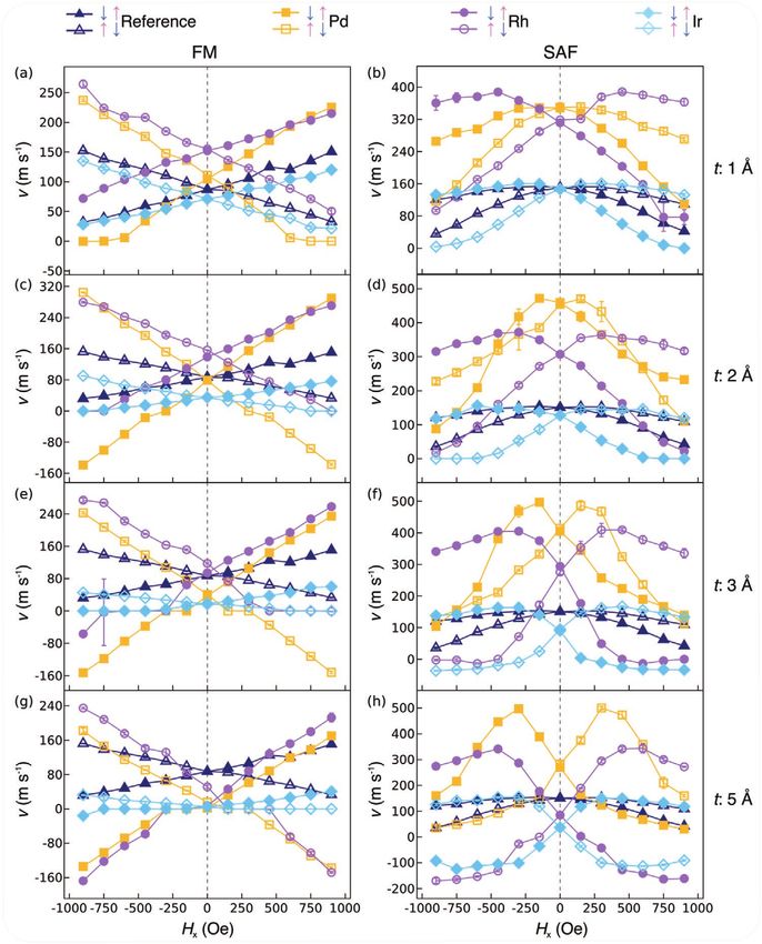
www.advancedsciencenews.com www.advmat.de
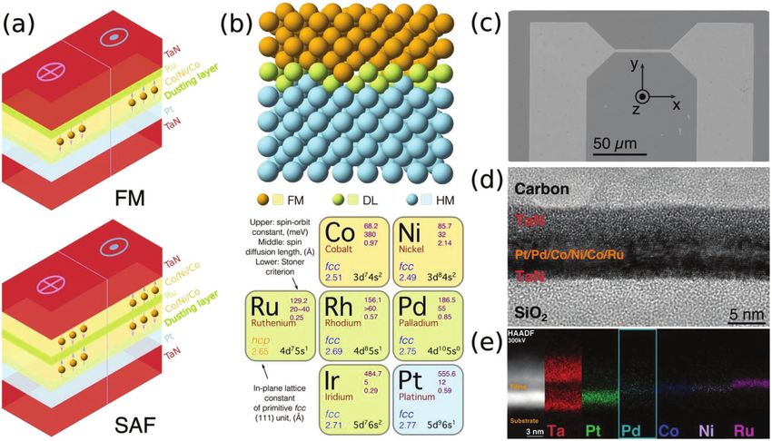
Figure 1. Engineered FM and SAF racetrack structures with interfacial dusting layers. a) Schematic representation of the FM (top) and SAF (bottom)
racetrack structures with a dusting layer (DL) inserted between the heavy metal (Pt) and ferromagnetic metal (Co) layers. b) Top: Schematic illustra-
tion of the atomic stack of the FM/DL/HM structure along the fcc (111) direction. Bottom: The color-coded elements employed in the FM/DL/HM
stack; orange, green, and light blue correspond to FM, DL, and HM, respectively. The numbers in the upper right position of each element square
correspond to (from top to bottom): the spin-orbit coupling constant, spin diffusion length, and Stoner criterion parameter, respectively. The number
in the lower-left position is the in-plane lattice constant of the corresponding fcc (111) unit. c) Scanning electron microscopy of a typical racetrack.
d) Cross-sectional HRTEM image, and e) the corresponding EDX mapping of an FM film with 1 Å thick Pd dusting layer, in which the presence of the
atomically thin Pd layer is highlighted.
dusting layers of selected 4d and 5d HMs at the ferromagnet/ thicknesses varying from 1 to 7 Å are inserted directly onto
platinum interface, a significant enhancement of the efficiency the Pt underlayer in both structures before the ferromagnetic
of the CIDWM is achieved for both single magnetic layer and materials are deposited. Schematic images of the FM and SAF
SAF racetrack structures. The Néel DWs move up to more structures are shown in Figure 1a with the elemental DLs illus-
than three times faster, for the same injected current density, trated in Figure 1b. The CIDWM was studied in racetracks of
compared to otherwise identical structures without any DL. 3 µm wide and 50 µm long, which were fabricated by photo-
Moreover, the threshold current density, Jth, defined as the lithography and Ar ion milling (Figure 1c).[10,15,19,22,31,32] The
minimum current density required to overcome effective pin- motion of individual DWs in these nanowires in response to
ning fields and move the DWs, can be substantially reduced by voltage pulses of a fixed length (≈10 ns) was detected using Kerr
incorporating atomically thin DLs. microscopy.[10,15,19] The DW positions in the nanowire before
and after the pulse injection are recorded and, thereby, used to
determine the DW velocity along the racetrack.
2. Results and Discussion A cross-sectional high-resolution transmission electron
microscopy (HRTEM) image of an FM structure with an ≈1 Å
Two sets of structures were prepared by DC magnetron sput- thick Pd DL is shown in Figure 1d. The image presents a highly
tering at room temperature, as shown in Figure 1a a ferro- (111) oriented structure of the face-centered-cubic (fcc) thin-
magnetic structure consisting of Co (3 Å)/Ni (7 Å)/Co (1.5 Å) film structure. The smooth surface of the films is confirmed
sandwiched between a Pt (15 Å) underlayer and an Ru (8.5 Å) by atomic force microscopy imaging (see Figure S1, Supporting
capping layer, hereafter referred to as an FM structure; and a Information). The high-angle annular dark-field scanning
synthetic antiferromagnet structure deposited on the same Pt TEM (HAADF-STEM) image and the associated energy-disper-
(15 Å) underlayer and consisting of a lower ferromagnetic layer sive X-ray spectrometry (EDX) maps of the layered structure
of Co (3 Å)/Ni (7 Å)/Co (1.5 Å) and an upper ferromagnetic layer in Figure 1e show that the Pd DL is at the expected location
of Co (5 Å)/Ni (7 Å)/Co (1.5 Å) antiferromagnetically exchange- between the Pt layer and the Co/Ni/Co layer, although the
coupled through an Ru (8.5 Å) spacer, hereafter referred to as EDX signal is obviously very weak, and moreover, is broadened
an SAF structure. A series of atomically thin layers (hereafter due to scattering processes and roughness of the individual
referred to as dusting layers, DL) of Pd, Ir, Rh, and Ru with layers.[33]
Adv. Mater. 2021, 33, 2007991 2007991 (2 of 9) © 2021 The Authors. Advanced Materials published by Wiley-VCH GmbH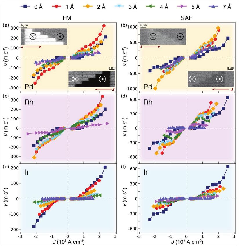
www.advancedsciencenews.com                                                                                                                    www.advmat.de

Figure 2. Interfacial DL engineered chiral domain wall motion in FM and SAF structures. a–f) Current-induced DW motion in the FM (left) and
SAF (right) structures with various DL materials: Pd ((a) and (b), orange background), Rh ((c) and (d), violet background), and Ir ((e) and (f), blue
background). The insets in (a) and (b) illustrate typical Kerr images of the domain wall motion in response to a series of injected current pulses
(≈1.0 × 10⁸ A cm−2) composed of, respectively, twelve (a) and four (b) 10 ns long pulses in the FM and SAF samples with 1 Å Pd DL, that confirms that
all the DWs move in the direction of current injection. Differences in image contrast originate from the magnetization difference in the FM and SAF sam-
ples. The bright and dark parts correspond to down (⊗ or ↓) and up (⊙ or ↑) domains. The thickness of the inserted dusting layers is varied from 0 Å
(navy squares), 1 Å (red circles), 2 Å (orange diamonds), 3 Å (light blue triangles), 4 Å (olive triangles), 5 Å (purple triangles), and 7 Å (orchid triangles).

   Distinct CIDWM behaviors are observed for the FM and                           CIDWM is improved for all Pd DL thicknesses considered
SAF structures that depend sensitively on the DL material and                     and is maximized for a Pd DL that is just ≈2 Å thick. The
thickness. Representative examples of CIDWM for DLs com-                          DW velocity is increased to ≈1000 m s−1 (Figure 2b), which is
posed of Pd, Rh, and Ir are shown in Figure 2. In all these                       ≈3.5 times higher than that of the reference SAF at the same
cases the DWs move along the direction of injected current,                       current density. For the Rh DL case the DW velocity is also
independent of the DL thickness. For the case of a sufficiently                   increased for ultra-thin DLs (1 and 2 Å) but the maximum v
thick Ru DL, however, the DWs are driven along the electron                       achieved was lower (≈600 m s−1).
flow direction, as discussed in the Supporting Information                           A significantly different behavior is observed when an Ir
(see Section S10 and Figure S16, Supporting Information). For                     DL is employed. In the FM case Jth drops when the DL is 1 Å
the case of both Pd and Rh DLs, Jth is significantly decreased                    thick, and then increases almost linearly with further increases
in the FM structure for DLs as thin as only 1 Å (Figure 2a,c),                    in Ir thickness (Figure 2e). Only a small enhancement in v
and the DW velocity, v, is increased for all current densities                    was observed at low current densities for 1 Å Ir, but otherwise
considered. For thicker DLs v is lower. The maximum cur-                          the CIDWM performance was worse than the reference FM
rent density that can be applied to the racetracks is limited by                  sample. For the SAF structure, a systematic deterioration of
the formation of multiple magnetic domains that we attribute                      the CIDWM occurs as soon as an Ir DL is inserted (Figure 2f).
to an increase in temperature of the nanowire, as has previ-                      However, it is worth noting that Jth drops smoothly for Ir DLs
ously been observed in nanowires of comparable resistance.[31]                    with thicknesses up to 5 Å but then increases dramatically for
By contrast, for the SAF structure, the performance of the                        thicker layers.

Adv. Mater. 2021, 33, 2007991                  2007991 (3 of 9)                            © 2021 The Authors. Advanced Materials published by Wiley-VCH GmbH
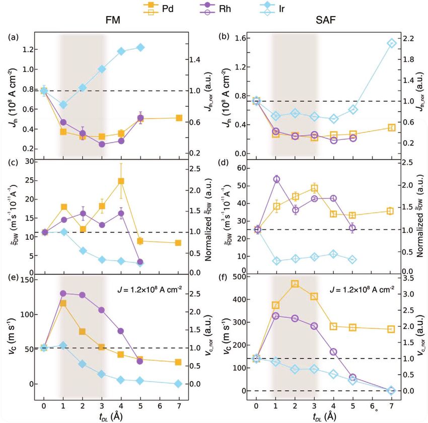
www.advancedsciencenews.com                                                                                                              www.advmat.de

Figure 3. DL thickness dependence of the DW velocity (v) and threshold current density (Jth). a,b) The threshold current density (Jth) as a function of
DL thickness in the FM and SAF samples. The dashed lines represent the threshold current density of the reference samples. The right axis represents
the normalized threshold current density (Jth_nor) with respect to the reference samples. c,d) The DW mobility (ξDW) around the threshold current in
the FM and SAF samples for various DL thicknesses (tDL). The dashed lines represent the DW mobility of the reference samples. e,f) The DW velocity
vC at a fixed current density (≈1.2 × 10⁸ A cm−2) in the FM and SAF samples with various DL thicknesses (tDL). The dashed lines represent the velocity
of the reference samples. The right axis is the normalized DW velocity (vc_nor) with respect to the reference samples. The colored regions illustrate the
interfacial DL thickness range, where the efficiency of CIDWM is maximized. Pd, Rh, and Ir DL correspond to orange squares, violet circles, and light
blue diamonds, respectively. The filled and open symbols correspond to the FM and SAF cases, respectively.

   To directly compare the influence of different DLs on the                  a monotonic drop in DW velocity is observed with increasing
CIDWM performance, i) Jth, ii) the DW mobility ξDW near Jth,                  tDL for Ir DLs (Figure 3e,f ).
which is derived from the slope of v versus current density J,                   The CIDWM is derived from a chiral spin torque, in which
and, iii) vC = v at J = 1.2 × 10⁸ A cm−2 are plotted as a function            the chirality of the DWs in both the FM and SAF structures is
of DL thickness tDL in Figure 3a–f for both the FM and SAF                    stabilized by an interfacial DMI arising from HM underlayers
structures. To distinguish CIDWM from DW creep that occurs                    with strong spin-orbit coupling.[15] Thus v depends sensitively
even at tiny current densities,[34] we define Jth as the cur-                 on magnetic fields applied along the racetrack:[10,15,19] external
rent density above which v exceeds 5 m s−1. For both the FM                   longitudinal magnetic fields Hx add or subtract from the DMI
and SAF cases, for Pd and Rh DLs, a decreased Jth together                    effective fields that stabilize the chiral DWs. v was measured as
with an increased ξDW is observed for thin DLs (1–4 Å), as                    a function of Hx. The movement of DWs with both ↓↑ and ↑↓
shown in Figure 3a–d. A decrease in Jth of up to 30% and an                   domain configurations with respect to Hx under positive current
increase in ξDW of more than 200% is found for both the FM                    are shown in Figure 4 in which racetracks incorporating Pd, Rh,
and SAF cases. For Ir DLs, although a slight decrease in Jth is               and Ir DLs with thicknesses of 1, 2, 3, and 5 Å are presented.
found for the thinnest DLs, substantial decreases in ξDW are                  Data are shown at a fixed current density (J = 1.2 × 10⁸ A cm−2).
observed for both FM and SAF structures. For Pd and Rh DLs                    Results for other DL thicknesses are given in the Supporting
the dependence of vC on tDL is similar for both the FM and                    Information (Figures S2 and S3, Supporting Information). For
SAF cases: vC initially increases significantly and then drops                the FM structure v depends linearly on Hx[15,19,22] with a slope
monotonically as tDL is increased from zero; by comparison,                   that strongly depends on the DL material and thickness, and

Adv. Mater. 2021, 33, 2007991                2007991 (4 of 9)                          © 2021 The Authors. Advanced Materials published by Wiley-VCH GmbH
www.advancedsciencenews.com                                                                                                           www.advmat.de

Figure 4. Longitudinal magnetic field dependence of DW velocity on the dusting layer. a–f) The longitudinal field dependence of DW velocity (v–Hx)
at a fixed current density (≈1.2 × 10⁸ A cm−2) in the FM (left) and SAF (right) structures. The open and filled symbols represent the ↑↓ and ↓↑ domain
configurations, respectively. The samples with DL thicknesses of 1 Å (a,b), 2 Å (c,d), 3 Å (e,f), and 5 A (g,h) are shown. Other DL thicknesses are
included in the Supporting Information (Figures S2 and S3, Supporting Information). The reference samples and those with Pd, Rh, and Ir DL are
represented by navy triangles, orange squares, violet circles, and light blue diamonds, respectively.

whose sign reverses for ↓↑ and ↑↓ DWs. This behavior can                    width of the DW does not change during its motion, and that the
be readily understood within a 1D DW analytical model of the                predominant SOT is damping-like, nevertheless such a model
chiral SOT:[15,19,35] there are two key characteristics: the slope of       has proven to be highly successful in accounting for the CIDWM
the v–Hx curve, and the magnitude of Hx where v = 0. By fitting             in many previous studies and in unravelling the underlying
these curves, the interfacial DMI strength D[19,35,36] can be deter-        physics.[10,15,19,21,23,24,35,36]
mined: the values of D thereby derived are given in Figure 5d. For               In order to interpret the influence of the DLs on the
the SAF case, the v–Hx curve has a more complex profile[10,21,32]           CIDWM, i) the saturation magnetization Ms, ii) the effective
but which can be understood within a 1D model that includes                 perpendicular magnetic anisotropy constant K ueff (defined as
the ECT in addition to the SOT. The detailed fits to the curves             K ueff = K − 2π MS2 = HKeff M s / 2, where K is the perpendicular
given in Figure 4b,d,f,h are discussed in the Supporting Informa-           magnetic anisotropy, and HKeff is the hard axis anisotropy field),
tion (Figures S4–S9, Supporting Information). Although the 1D               and iii) the ratio of the remnant magnetization (magnetiza-
model makes some assumptions, in particular, that the form and              tion at ≈0 T, Mr) to saturation magnetization (magnetization

Adv. Mater. 2021, 33, 2007991               2007991 (5 of 9)                         © 2021 The Authors. Advanced Materials published by Wiley-VCH GmbH
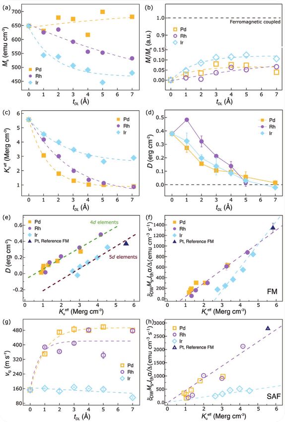
www.advancedsciencenews.com                                                                                                                www.advmat.de

Figure 5. Interfacial dusting layer engineered magnetic properties. a–c) The DL thickness dependence of: (a) saturation magnetization of the FM structures,
(b) remnant magnetization to saturation magnetization ratio for the SAF structures, (c) effective uniaxial anisotropy constant K ueff for the FM structures,
d) D calculated from the FM cases. e) D of FM samples plotted as a function of K ueff , in which the dashed lines are linear fits for the groups of DLs
formed from 4d elements (Pd and Rh, olive) and 5d elements (Ir and Pt, brown), respectively. The Pt data point corresponds to the reference sample
without any DL. f,h) Dependence of αξDWMSJth/Δ on K ueff for FM and SAF cases, respectively. The dashed lines are linear fits for the groups of DLs
formed from 4d elements (Pd and Rh, violet) and 5d elements (Ir and Pt, light blue), respectively. The Pt data point corresponds to the reference
sample without any DL. g) DL thickness dependence of the DW peak velocity vlg extracted from the v–Hx curves for the SAF structures in Figure 4 and
Figure S3, Supporting Information. The filled and open symbols correspond to the FM and SAF cases, respectively.

field ≈ 1.5 T) Mr/Ms in the SAF structures, were measured.                      increasing tDL in all cases (Figure 5c). Ms varies little with Pd
The dependence of these parameters on tDL are plotted in                        DL, while a monotonic drop for the Ir and Rh DLs cases is
Figure 5a,c. A monotonic drop in K ueff can be observed with                    observed (Figure 5a). Proximity induced magnetic moments

Adv. Mater. 2021, 33, 2007991                 2007991 (6 of 9)                          © 2021 The Authors. Advanced Materials published by Wiley-VCH GmbH
www.advancedsciencenews.com                                                                                                       www.advmat.de

(PIM) in heavy metals can contribute considerably to the Ms of           and SAF cases show two distinct linear relationships for 4d DLs,
ferromagnet/HM systems.[19,37] Based on the Stoner criterion             on the one hand, and 5d DLs, on the other hand (Figure 5f,h).
(Figure 1b), it would not be surprising if the PIM decreases             Thus, the threshold spin current is linearly related to K ueff for
when the Ir and Rh DLs are inserted between the Co and Pt                both the FM and SAF cases and can be reduced by introduction
layers. On the other hand, we suppose that there may be a con-           of suitable DLs.
siderable PIM in the Pd DL itself since Pd is very close to the             For the practical application of racetrack memory devices,
Stoner criteria for magnetism.[38]                                       low Jth, high ξDW, and high v are required. For the FM case,
   To demonstrate that the effect of the DL on the CIDMW is              the linear dependence of K ueff on D shows that once a smaller
interfacial and is not a volume effect, a set of FM structures was       Jth is realized through decreasing K ueff , the saturation DW v at
prepared in which a 2 Å DL is systematically moved parallel to           high current density is also decreased due to a smaller D.[35]
the film normal away from the Co/Pt interface into the interior          However, at currents just above the threshold current, the DW
of the Pt underlayer. The influence of the ultrathin DL on the           velocity is higher than otherwise would be the case. By contrast,
magnetic properties and the CIDWM is clearly effective only              for the SAF case, a low Jth and high v can both be achieved
when located at or very near (
www.advancedsciencenews.com                                                                                                                www.advmat.de

that generating DWs by alternative external field-free methods would be        [1] a) D. A. Allwood, G. Xiong, C. Faulkner, D. Atkinson, D. Petit,
favored.[40]                                                                       R. Cowburn, Science 2005, 309, 1688; b) S. S. P. Parkin, S.-H. Yang,
   TEM Specimen Preparation and Investigation: Cross-sectional TEM                 Nat. Nanotechnol. 2015, 10, 195.
specimens were formed by conventional preparation methods using               [2] a) S. Bader, S. S. P. Parkin, Annu. Rev. Condens. Matter Phys. 2010,
mechanical polishing (both sides), dimple-grinding (one side) and                  1, 71; b) J. Torrejon, M. Riou, F. A. Araujo, S. Tsunegi, G. Khalsa,
thinned down for electron transparency by polishing with Ar ions at 5 kV           D. Querlioz, P. Bortolotti, V. Cros, K. Yakushiji, A. Fukushima,
in a Gatan PIPS (precision ion polishing system) system. For HRTEM/                Nature 2017, 547, 428.
STEM investigations, an FEI TITAN 80–300 electron microscope with a           [3] S. S. P. Parkin, M. Hayashi, L. Thomas, Science 2008, 320, 190.
probe corrector was used at an accelerating voltage of 300 kV. The EDX
                                                                              [4] W. Jiang, P. Upadhyaya, W. Zhang, G. Yu, M. B. Jungfleisch,
experiments were performed with a Super-X detector system (4 silicon
                                                                                   F. Y. Fradin, J. E. Pearson, Y. Tserkovnyak, K. L. Wang, O. Heinonen,
drift detectors placed symmetrically around the sample area inside the
                                                                                   Science 2015, 349, 283.
objective lens) installed on the microscope for improved efficiency of
X-ray collection. Acquired EDX maps were analyzed and processed by            [5] A. K. Nayak, V. Kumar, T. Ma, P. Werner, E. Pippel, R. Sahoo,
Bruker Esprit software.                                                            F. Damay, U. K. Rößler, C. Felser, S. S. P. Parkin, Nature 2017, 548, 561.
   Magnetic Property Measurements and Calculation of DMI Constant D:          [6] a) S. Fukami, in Symp. on VLSI Technology Digest of Technical Papers,
The sample magnetization was measured in a superconducting quantum                 IEEE, Piscataway, NJ, USA 2009, p. 230; b) J. Grollier, P. Boulenc,
interference device (SQUID) magnetometer at room temperature.                      V. Cros, A. Hamzić, A. Vaurès, A. Fert, G. Faini, Appl. Phys. Lett.
HKeff , the field where the magnetization is rotated from out-of-plane to          2003, 83, 509; c) A. Yamaguchi, T. Ono, S. Nasu, K. Miyake,
in-plane, was measured using a vibrating sample magnetometer. Mr and               K. Mibu, T. Shinjo, Phys. Rev. Lett. 2004, 92, 077205; d) L. Thomas,
Ms of the SAF samples were determined at fields of 0 Oe and 15 kOe,                M. Hayashi, X. Jiang, R. Moriya, C. Rettner, S. S. P. Parkin, Nature
respectively, from out-of-plane M–H curves (Figure S14, Supporting                 2006, 443, 197; e) M. Hayashi, L. Thomas, C. Rettner, R. Moriya,
Information). The Gilbert damping parameter α was obtained from                    Y. B. P. Bazaliy, S. S. P. Parkin, Phys. Rev. Lett. 2007, 98, 037204.
Optical Ferromagnetic Resonance measurements. The DW width was                [7] A. Fert, V. Cros, J. Sampaio, Nat. Nanotechnol. 2013, 8, 152.
calculated from ∆ = A / K ueff with A, the exchange stiffness, set to be      [8] M. Hayashi, L. Thomas, R. Moriya, C. Rettner, S. S. Parkin, Science
a constant of 1.0 μerg cm−1.[32] The DMI constant D was calculated from            2008, 320, 209.
the expression D = μ0 MsΔHDMI[35] where HDMI was determined from the          [9] R. A. Duine, K. J. Lee, S. S. P. Parkin, M. D. Stiles, Nat. Phys. 2018,
dependence of the DW velocity on an in-plane magnetic field.                       14, 217.
                                                                            [10] S.-H. Yang, K.-S. Ryu, S. S. P. Parkin, Nat. Nanotechnol. 2015, 10, 221.
                                                                             [11] I. M. Miron, G. Gaudin, S. Auffret, B. Rodmacq, A. Schuhl,
                                                                                   S. Pizzini, J. Vogel, P. Gambardella, Nat. Mater. 2010, 9, 230.
Supporting Information                                                      [12] A. Thiaville, Y. Nakatani, J. Miltat, Y. Suzuki, Europhys. Lett. 2005,
Supporting Information is available from the Wiley Online Library or               69, 990.
from the author.                                                             [13] I. M. Miron, T. Moore, H. Szambolics, L. D. B.-Prejbeanu, S. Auffret,
                                                                                   B. Rodmacq, S. Pizzini, J. Vogel, M. Bonfim, A. Schuhl, G. Gaudin,
                                                                                   Nat. Mater. 2011, 10, 419.
                                                                             [14] L. Liu, O. J. Lee, T. J. Gudmundsen, D. C. Ralph, R. A. Buhrman,
Acknowledgements                                                                   Phys. Rev. Lett. 2012, 109, 096602.
                                                                            [15] K.-S. Ryu, L. Thomas, S.-H. Yang, S. S. P. Parkin, Nat. Nanotechnol.
Y.G. and X.Z. contributed equally to this work. This project received
                                                                                   2013, 8, 527.
funding from the European Research Council (ERC) under the
                                                                            [16] A. Manchon, S. Zhang, Phys. Rev. B 2008, 78, 212405.
European Union’s Horizon 2020 research and innovation program
(grant agreement no. 670166). This project also received funding from        [17] M. Bode, M. Heide, K. von Bergmann, P. Ferriani, S. Heinze,
the European Union’s Horizon 2020 research and innovation program                  G. Bihlmayer, A. Kubetzka, O. Pietzsch, S. Blügel, R. Wiesendanger,
under grant agreement no. 766566.                                                  Nature 2007, 447, 190.
   Open access funding enabled and organized by Projekt DEAL.               [18] a) I. Dzyaloshinsky, J. Phys. Chem. Solids 1958, 4, 241; b) T. Moriya,
                                                                                   Phys. Rev. 1960, 120, 91.
                                                                            [19] K.-S. Ryu, S.-H. Yang, L. Thomas, S. S. P. Parkin, Nat. Commun.
                                                                                   2014, 5, 3910.
Conflict of Interest                                                        [20] a) C. Garg, S.-H. Yang, T. Phung, A. Pushp, S. S. P. Parkin, Sci.
                                                                                   Adv. 2017, 3, e1602804; b) C. Garg, A. Pushp, S.-H. Yang, T. Phung,
The authors declare no conflict of interest.                                       B. P. Hughes, C. Rettner, S. S. P. Parkin, Nano Lett. 2018, 18,
                                                                                   1826.
                                                                            [21] S. -H. Yang, S. S. P. Parkin., J. Phys.: Condens. Matter 2017, 29, 303001.
                                                                            [22] R. Bläsing, T. Ma, S. H. Yang, C. Garg, F. K. Dejene, A. T. N’Diaye,
Data Availability Statement
                                                                                   G. Chen, K. Liu, S. S. P. Parkin, Nat. Commun. 2018, 9, 4984.
The data that support the findings of this study are available from the     [23] L. Caretta, M. Mann, F. Büttner, K. Ueda, B. Pfau, C. M. Günther,
corresponding author upon reasonable request.                                      P. Hessing, A. Churikova, C. Klose, M. Schneider, D. Engel,
                                                                                   C. Marcus, D. Bono, K. Bagschik, S. Eisebitt, G. S. D. Beach, Nat.
                                                                                   Nanotechnol. 2018, 13, 1154.
                                                                            [24] a) C. O. Avci, E. Rosenberg, L. Caretta, F. Büttner, M. Mann,
Keywords                                                                           C. Marcus, D. Bono, C. A. Ross, G. S. Beach, Nat. Nanotechnol.
dusting layers, Dzyaloshinskii–Moriya interaction, racetrack memory,               2019, 14, 561; b) S. Vélez, J. Schaab, M. S. Wörnle, M. Müller,
synthetic antiferromagnets                                                         E. Gradauskaite, P. Welter, C. Gutgsell, C. Nistor, C. L. Degen,
                                                                                   M. Trassin, M. Fiebig, P. Gambardella, Nat. Commun. 2019, 10,
                                           Received: November 25, 2020             4750.
                                             Revised: December 28, 2020     [25] G. Chen, T. Ma, A. T. N’Diaye, H. Kwon, C. Won, Y. Wu,
                                       Published online: February 4, 2021          A. K. Schmid, Nat. Commun. 2013, 4, 2671.

Adv. Mater. 2021, 33, 2007991                  2007991 (8 of 9)                      © 2021 The Authors. Advanced Materials published by Wiley-VCH GmbH
www.advancedsciencenews.com www.advmat.de
[26] a) A. Soumyanarayanan, N. Reyren, A. Fert, C. Panagopoulos, J. P. Jamet, A. Mougin, M. Cormier, J. Ferre, V. Baltz, B. Rodmacq,
Nature 2016, 539, 509; b) W. Zhang, W. Han, X. Jiang, S.-H. Yang, B. Dieny, R. L. Stamps, Phys. Rev. Lett. 2007, 99, 217208.
S. S. P. Parkin, Nat. Phys. 2015, 11, 496. [35] A. Thiaville, S. Rohart, É. Jué, V. Cros, A. Fert, Europhys. Lett. 2012,
[27] a) J. Torrejon, J. Kim, J. Sinha, S. Mitani, M. Hayashi, 100, 57002.
M. Yamanouchi, H. Ohno, Nat. Commun. 2014, 5, 4655; b) X. Qiu, [36] S. Emori, U. Bauer, S. M. Ahn, E. Martinez, G. S. D. Beach, Nat.
W. Legrand, P. He, Y. Wu, J. Yu, R. Ramaswamy, A. Manchon, Mater. 2013, 12, 611.
H. Yang, Phys. Rev. Lett. 2016, 117, 217206. [37] I. Žutić, A. Matos-Abiague, B. Scharf, H. Dery, K. Belashchenko,
[28] a) J. Cho, N.-H. Kim, S. Lee, J.-S. Kim, R. Lavrijsen, A. Solignac, Mater. Today 2019, 22, 85.
Y. Yin, D.-S. Han, N. J. van Hoof, H. J. Swagten, Nat. Commun. [38] a) S. Sakuragi, T. Sakai, S. Urata, A. Aihara, A. Shinto, H. Kageshima,
2015, 6, 7635; b) J. Kim, J. Sinha, M. Hayashi, M. Yamanouchi, M. Sawada, H. Namatame, M. Taniguchi, T. Sato, Phys. Rev. B 2014,
S. Fukami, T. Suzuki, S. Mitani, H. Ohno, Nat. Mater. 2013, 12, 240. 90, 054411; b) T. Moriya, Spin Fluctuations in Itinerant Electron Mag-
[29] S. S. P. Parkin, Phys. Rev. Lett. 1993, 71, 1641. netism, Vol. 56, Springer Science & Business Media, New York 2012.
[30] a) V. M. Parakkat, K. R. Ganesh, P. S. A. Kumar, AIP Adv. 2016, [39] a) S. Kim, K. Ueda, G. Go, P. H. Jang, K. J. Lee, A. Belabbes,
6, 056118; b) A. G. Kolesnikov, A. V. Ognev, M. E. Stebliy, A. Manchon, M. Suzuki, Y. Kotani, T. Nakamura, K. Nakamura,
L. A. Chebotkevich, A. V. Gerasimenko, A. S. Samardak, J. Magn. T. Koyama, D. Chiba, K. T. Yamada, D. H. Kim, T. Moriyama, K. J. Kim,
Magn. Mater. 2018, 454, 78; c) A. Kaidatzis, C. Bran, V. Psycharis, T. Ono, Nat. Commun. 2018, 9, 1648; b) X. Ma, G. Q. Yu, C. Tang,
M. Vazquez, J. M. Garcia-Martin, D. Niarchos, Appl. Phys. Lett. 2015, X. Li, C. L. He, J. Shi, K. L. Wang, X. Q. Li, Phys. Rev. Lett. 2018, 120,
106, 262401; d) C. F. Pai, M. H. Nguyen, C. Belvin, L. H. Vilela-Leao, 157204; c) V. Kashid, T. Schena, B. Zimmermann, Y. Mokrousov,
D. C. Ralph, R. A. Buhrman, Appl. Phys. Lett. 2014, 104, 082407; S. Blugel, V. Shah, H. G. Salunke, Phys. Rev. B 2014, 90,
e) H. Almasi, M. Xu, Y. Xu, T. Newhouse-Illige, W. G. Wang, 054412.
Appl. Phys. Lett. 2016, 109, 032401; f) C. O. Avci, G. S. D. Beach, [40] a) Y. Sheng, K. W. Edmonds, X. Q. Ma, H. Z. Zheng, K. Y. Wang,
P. Gambardella, Phys. Rev. B 2019, 100, 235454. Adv. Electron. Mater. 2018, 4, 1800224; b) K. M. Cai, M. Y. Yang,
[31] K.-S. Ryu, L. Thomas, S.-H. Yang, S. S. P. Parkin, Appl. Phys. Express H. L. Ju, S. M. Wang, Y. Ji, B. H. Li, K. W. Edmonds, Y. Sheng,
2012, 5, 093006. B. Zhang, N. Zhang, S. Liu, H. Z. Zheng, K. Y. Wang, Nat.
[32] S.-H. Yang, C. Garg, S. S. P. Parkin, Nat. Phys. 2019, 15, 543. Mater. 2017, 16, 712; c) S. Fukami, C. L. Zhang, S. DuttaGupta,
[33] G. Kothleutner, M. J. Neish, N. R. Lugg, S. D. Findlay, W. Grogger, A. Kurenkov, H. Ohno, Nat. Mater. 2016, 15, 535;
F. Hofer, L. J. Allen, Phys. Rev. Lett. 2014, 112, 085501. d) S. H. C. Baek, V. P. Amin, Y. W. Oh, G. Go, S. J. Lee, G. H. Lee,
[34] a) L. S. E. Alvarez, K.-Y. Wang, S. Lepadatu, S. Landi, S. J. Bending, K. J. Kim, M. D. Stiles, B. G. Park, K. J. Lee, Nat. Mater. 2018, 17,
C. Marrows, Phys. Rev. Lett. 2010, 104, 137205; b) P. J. Metaxas, 509.
Adv. Mater. 2021, 33, 2007991 2007991 (9 of 9) © 2021 The Authors. Advanced Materials published by Wiley-VCH GmbHYou can also read