Investigation of Nitrogen and Vacancy Defects in Synthetic Diamond Plates by Positron Annihilation Spectroscopy - MDPI
←
→
Page content transcription
If your browser does not render page correctly, please read the page content below

materials
Article
Investigation of Nitrogen and Vacancy Defects in Synthetic
Diamond Plates by Positron Annihilation Spectroscopy
Marat Eseev 1, * , Ivan Kuziv 1 , Aleksey Kostin 1 , Igor Meshkov 2 , Aleksey Sidorin 2 and Oleg Orlov 2

 1 Northern (Arctic) Federal University, 17 Severnoi Dviny emb., 163002 Arkhangelsk, Russia
 2 Joint Institute for Nuclear Research, 6 Joliot-Curie Str., 141980 Dubna, Russia
 * Correspondence: m.eseev@narfu.ru

 Abstract: Currently, diamonds are widely used in science and technology. However, the properties
 of diamonds due to their defects are not fully understood. In addition to optical methods, positron
 annihilation spectroscopy (PAS) can be successfully used to study defects in diamonds. Positrons are
 capable of detecting vacancies, and small and large clusters of vacancies induced by irradiation, by
 providing information about their size, concentration, and chemical environment. By mapping in
 the infrared (IR) range, it is possible to consider the admixture composition of the main inclusions
 of the whole plate. This article presents the results of a study of defects in synthetic diamond
 plates, one of which was irradiated by electrons. It presents data about the distribution of the defect
 concentration obtained by Infrared spectroscopy. PAS with a monochromatic positron beam can be
 used as a non-destructive technique of detecting defects (vacancy) distribution over the depth of
 diamond plates.

 Keywords: NV-centers; positron annihilation spectroscopy; IR-spectroscopy; defects; vacancy;
 diamonds; unbreakable control

 1. Introduction
Citation: Eseev, M.; Kuziv, I.; Kostin,
A.; Meshkov, I.; Sidorin, A.; Orlov, O.
 The diamond is the most promising wide band semiconductor [1] due to its cubic
Investigation of Nitrogen and crystal structure and strong covalent bonds of carbon atoms, as well as its record high
Vacancy Defects in Synthetic atomic density. However, many unique properties and prospects for high-tech applications
Diamond Plates by Positron of diamonds [2] are determined by the presence and concentration of various types of its
Annihilation Spectroscopy. Materials lattice defects.
2023, 16, 203. https://doi.org/ At the crystal lattice level, such defects can be zero-dimensional, one-dimensional, two-
10.3390/ma16010203 dimensional or three-dimensional. Zero-dimensional defects include point defects such as
 vacancies, impurity substitutions, and introductions. The presence of defects in diamond
Academic Editor: Valery
N. Khabashesku
 drastically affects its physical properties, the mechanical, thermophysical, electromagnetic
 and quantum properties of diamond change.
Received: 16 November 2022 In practical terms, the presence and concentration of defects can be both negative
Revised: 17 December 2022 and positive factors. In the first case, their detection helps to cull products and improve
Accepted: 21 December 2022 the technological processes of diamond manufacturing. In the second case, varying the
Published: 26 December 2022
 concentration of defects allows for obtaining unique diamond properties. One such unique
 property of diamonds is the possibility to manipulate spins of single atoms related to
 impurity defects and to read them with the help of optical methods [3].
Copyright: © 2022 by the authors.
 The methods of manipulating spins in combination with methods of growing high-
Licensee MDPI, Basel, Switzerland. quality diamonds are already leading to the creation of quantum devices and applications
This article is an open access article such as resonant Forster energy transfer [4] and single-spin magnetometry [5], as well
distributed under the terms and as new methods for obtaining images with unsurpassed resolution [6–8]. The interest in
conditions of the Creative Commons defects in diamonds and the mechanisms of their transformation seems to be relevant
Attribution (CC BY) license (https:// from the point of view of fundamental science and for the development of technologies for
creativecommons.org/licenses/by/ obtaining high-pressure/high-temperature (HPHT) and chemical vapor deposition (CVD)
4.0/). diamond single crystals with specified properties.

Materials 2023, 16, 203. https://doi.org/10.3390/ma16010203 https://www.mdpi.com/journal/materials
Materials 2023, 16, 203 2 of 10

 Defects of the vacancy type are the most interesting of all crystal lattice defects. One
 such defect is the nitrogen-vacancy-center (NV-center). The NV-center is a type of point
 defect in a diamond in which one carbon atom in the crystal lattice of a diamond is replaced
 by a nitrogen atom, and the neighboring lattice node remains vacant. Such an NV-center
 was first identified by Du Pre in 1965 [9], and the first important optical characteristics of
 such a center were described by Davis and Hamer in 1976 [10]. The first work in which
 single NV-centers were observed was published in 1997 [11]. After the discovery of single
 negatively charged centers, it was possible to demonstrate the photostable generation
 of single photons [12,13], which allowed the use of NV-centers in the implementation
 of quantum optical networks, as well as for electron spin readout [14,15], which defines
 such an NV-center as a possible solid state spin cubit, suitable for quantum information
 processing and applications in quantum sensing.
 Known methods for studying natural and synthetic diamonds include the following:
 • Vibrational spectroscopy (Raman and infrared spectroscopy, photoluminescence; ab-
 sorption spectroscopy in the visible and UV regions).
 • X-ray and neutron methods: small-angle scattering, topography, absorption spec-
 troscopy (X-ray Absorption Fine Structure spectroscopy-XAFS).
 • Nuclear physics methods: nuclear reaction method (Nuclear Reaction Analysis-
 NRA), and analysis of recoil nuclei (Elastic Recoil Detection Analysis-ERDA); positron
 spectroscopy.
 • Secondary ion mass spectrometry (SIM) and thermal desorption.
 • Microscopy and microprobe analysis.
 Electron paramagnetic resonance (EPR) and optically detected magnetic resonance
 (ODMR) are used to diagnose NV centers.
 We used a comparison of the generally accepted method of IR spectroscopy with PAS.
 The advantage of the latter is the high sensitivity of the method to single-crystal lattice
 defects at the level of 0.1 ppm and the possibility of scanning along the sample depth (z)
 (see, for example, [16]).
 Today, positron annihilation spectroscopy, along with optical methods, is a relevant
 method for the study of NV-centers. This research method is extremely sensitive to the
 detection of defects at the crystal lattice level. The wide application of this method for the
 study of defects in semiconductors began in 1980 [17], and the first papers on the study
 of vacancy-type defects in diamonds were published in 2000 [18]. Positron annihilation
 spectroscopy can be realized by three methods: the method of positron annihilation lifetime
 spectroscopy method, the positron annihilation Doppler broadening spectroscopy method,
 and the angular correlation of radiation method [19,20].
 The unique possibilities of non-destructive testing can be obtained using a monochro-
 matic positron beam [21]. By changing its energy, it is possible to scan samples for the
 presence of defects in depth with extremely high accuracy. This method has been success-
 fully used to analyze crystalline materials [22,23] for the appearance of vacancies under
 mechanical stress. PAS studies are used for semiconductors, metals, carbon nanostructures,
 and minerals (see, for example, [24,25]).
 In this article, we studied the defects in nitrogen doped synthetic diamond plates which
 arise during electron irradiation. The main goal of the study focused on the determination
 of the type and concentration of defects. Infrared spectroscopy was used to determine
 the concentration of nitrogen and defects after irradiation, while positron annihilation
 spectroscopy was used to determine the presence of defects before and after irradiation.
 Subsurface defects in diamond plates and their depth profile were investigated using the
 Doppler annihilation line broadening method.

 2. Experiment
 The experiment was performed on two synthetic diamond plates (SAFU01 and
 SAFU02). The synthetic diamond plates were grown by HTHP technology using the
 temperature gradient method. The samples were then cut by laser with a side size of
2. Experiment
 The experiment was performed on two synthetic diamond plates (SAFU01 and
Materials 2023, 16, 203 3 of 10
 SAFU02). The synthetic diamond plates were grown by HTHP technology using the tem-
 perature gradient method. The samples were then cut by laser with a side size of 4 × 4 mm
 and a height of 1.5 mm. The condition of the samples before electron irradiation was
 4 × 4 mm
 checked byand a height
 infrared of 1.5 mm.and
 spectroscopy Thethecondition
 Doppler of the samples
 annihilation before
 line electronmethod.
 broadening irradia-
 tion was checked by infrared spectroscopy and the Doppler annihilation line
 One sample (SAFU02) was left as a reference, the non-irradiated specimen. The SAFU01 broadening
 method.
 sample One
 was sample
 then (SAFU02)
 irradiated withwas left as aofreference,
 an energy the non-irradiated
 10 MeV electrons specimen.
 up to a dose The
 of 1.1 × 10 16
 SAFU01 sample was then irradiated with an energy of 10 MeV electrons up to a dose of
 cm−2. No16defects after such a dose of irradiation were noted. Furthermore, the SAFU01
 1.1 × 10 cm−2 . No defects after such a dose of irradiation were noted. Furthermore, the
 sample was again irradiated by electrons (3 MeV, 1 × 10¹⁸/cm2). 18
 SAFU01 sample was again irradiated by electrons (3 MeV, 1 × 10 /cm2 ).
 3.3.Methods
 Methods
 The
 Thesamples
 sampleswere wereinvestigated
 investigatedby byan aninfrared
 infraredspectrometer,
 spectrometer,aaSHIMADZU
 SHIMADZUUV UV3600i
 3600i
 Plus
 Plus (SHIMADZU, Kyoto, Japan), and by the Doppler annihilation line broadeningtech-
 (SHIMADZU, Kyoto, Japan), and by the Doppler annihilation line broadening tech-
 nique
 nique ofof Positron Annihilation Spectroscopy.
 Positron Annihilation Spectroscopy.The Themeasurement
 measurementofof thethe Doppler
 Doppler annihila-
 annihilation
 tion
 line line broadening
 broadening waswas performed
 performed usingusing
 the the ORTEC
 ORTEC HPGe HPGe detector
 detector (model
 (model GEM25P4-
 GEM25P4-70).
 70). Doppler
 Doppler spectroscopy
 spectroscopy waswas implemented
 implemented on aon a positron
 positron beam beam facility
 facility withwith energy
 energy var-
 variation
 iation
 from 0.1 to 30 keV. The positrons were emitted directly from the source of the isotope iso-
 from 0.1 to 30 keV. The positrons were emitted directly from the source of the 22 Na.
 tope 22Na. The flux intensity
 The flux intensity was 106 e+ /s, wasand 106 the
 e+/s,beam
 and the
 spotbeam spot was
 diameter diameter was approximately
 approximately 5 mm. The
 5value
 mm. of The 2.5value
 × 105ofcounts
 2.5 × 10 5 counts at the 511 keV annihilation peak.
 at the 511 keV annihilation peak.
 The
 The Doppler broadeningof
 Doppler broadening ofannihilation
 annihilationline linemethod
 methodisisused
 usedto todetect
 detectconcentrations
 concentrations
 of
 ofdefects
 defectssuchsuchasasvacancies
 vacanciesand andvacancy
 vacancy accumulations.
 accumulations. A signal
 A signal fromfromthethe
 annihilation
 annihilation of
 aoftrapped
 a trapped positron
 positron gives
 givesa broadening
 a broadening ofof
 the
 the511
 511keVkeVline
 linewhich
 whichisisaccordingly
 accordinglysmaller
 smaller
 than
 than the
 the oneone that
 that would
 would occur
 occur in in case
 case of annihilation
 annihilation withwith nucleus
 nucleus electrons.
 electrons. In In other
 other
 words, more defective sample gives a larger broadening of the 511
 words, more defective sample gives a larger broadening of the 511 keV line. Each obtained keV line. Each obtained
 spectrum
 spectrumwas wasanalyzed
 analyzedtoto calculate
 calculate parameters
 parameters S and W (Figure
 S and W (Figure1) using the SP-16K
 1) using pro-
 the SP-16K
 gram
 program[26].[26].
 Parameter
 ParameterS reflects annihilations
 S reflects annihilationsof low-momentum
 of low-momentum electrons occurring
 electrons occurringin de-in
 fects. It isItsensitive
 defects. is sensitiveto open
 to open volume
 volume defects
 defectssuch
 suchasasvacancies
 vacancies andandvacancy
 vacancyaccumulations.
 accumulations.
 Parameter
 ParameterSSisisdefined
 defined as asthe
 theratio
 ratioof ofthe
 thearea
 areabelow
 belowthe thecentral
 central part
 part(A (ASSwithin
 withinthetheenergy
 energy
 range
 rangeof of511511±± 1.03 keV)
 1.03 keV) ofof
 thetheannihilation
 annihilation line to the
 line total
 to the area
 total in the
 area range
 in the of this
 range lineline
 of this (A
 (A within
 within the energy
 the energy range range
 of 511 10.3±keV).
 of ±511 10.3 keV).
 A larger A larger
 value of value of parameter
 parameter S means S means
 a largera
 larger concentration
 concentration of defectsof in
 defects in the sample.
 the sample. Parameter Parameter
 W reflects Wannihilations
 reflects annihilations of high-
 of high-momen-
 momentum
 tum electronselectrons and it provides
 and it provides information information
 about the about the chemical
 chemical environment environment of the
 of the defect.
 defect.
 This This parameter
 parameter can indicatecanaindicate
 change in a change in the appearance
 the appearance or size
 or size of lattice of lattice
 defects. defects.
 Parameter
 WParameter
 is given as Wtheis given as the
 ratio of the area
 ratiounder
 of the the
 areawing
 under the(Awing
 part part (A
 W—within W —within
 the the energy
 energy range from
 range
 511 from
 ± 3.44 keV511to± 5113.44 keVkeV)
 ± 10.3 to 511 of ±the10.3
 511 keV) of the
 keV line 511 total
 to the keV arealine to(A)the total area
 marked by that(A)
 marked
 line. by that line.

 Figure 1. 511 keV lines for defective and non-defective samples.
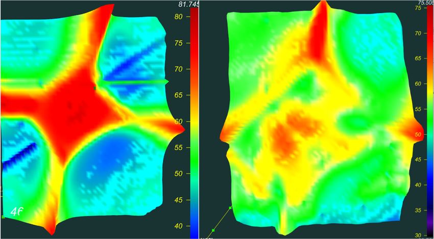
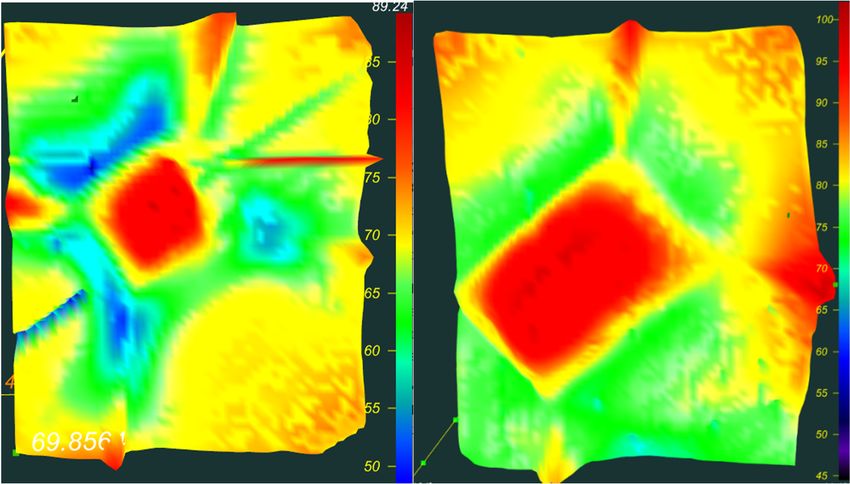
Materials 2023, 16, x FOR PEER REVIEW 4 of 10

 Materials 2023, 16, 203 Figure 1. 511 keV lines for defective and non-defective samples. 4 of 10

 The Doppler broadening of the annihilation line method is based on a slow monoen-
 ergetic
 Thepositron
 Doppler beam with energies
 broadening up to 30 keV
 of the annihilation line located
 method at the Joint
 is based on aInstitute for Nuclear
 slow monoener-
 Research
 getic in Dubna,
 positron Russia.
 beam with energies up to 30 keV located at the Joint Institute for Nuclear
 Research in Dubna, Russia.
 4. Distribution Maps of IR Spectroscopy
 4. Distribution Maps of IR Spectroscopy
 In this paragraph, a yellow diamond plate SAFU01 was studied. The distribution
 In this paragraph, a yellow diamond plate SAFU01 was studied. The distribution maps
 maps of the main defects were obtained using a MIKRAN-3 spectrometer with a photo-
 of the main defects were obtained using a MIKRAN-3 spectrometer with a photodetector −1
 detector cooled in liquid nitrogen in the IR range of wave numbers from 1000 to 1500 cm .
 cooled in liquid nitrogen in the IR range of wave numbers from 1000 to 1500 cm−1 .
 Beforestarting
 Before startingthe
 theexperiment,
 experiment,the the sample
 sample surface
 surface was was cleaned
 cleaned withwith ethyl
 ethyl alcohol.
 alcohol.
 The best area for mapping was selected. The size of the area was 2311 by 2889 µm. The The
 The best area for mapping was selected. The size of the area was 2311 by 2889 µm.
 scanningstep
 scanning stepwaswas41.275
 41.275µm.µm.TheThe beam
 beam size
 size was
 was corrected
 corrected by the
 by the aperture,
 aperture, and and the beam
 the beam
 areawas
 area was5050byby5050µm.
 µm.
 Thefollowing
 The followingarearemaps
 maps ofof
 thethe defect
 defect distribution.
 distribution. TheThe vertical
 vertical scalescale is transmittance
 is transmittance
 registered as a percentage.
 registered as a percentage.
 Figure22shows
 Figure showsthetheIRIRspectrum
 spectrum of of a yellow
 a yellow diamond
 diamond withwith
 the the distribution
 distribution of C-defect
 of C-defect
 (defect
 (defect C,
 C,orordonor
 donornitrogen,
 nitrogen,is is
 a single
 a single nitrogen atom
 nitrogen thatthat
 atom isomorphically
 isomorphically replaces the the
 replaces
 carbon atom in the diamond lattice):
 carbon atom in the diamond lattice):

 Figure2.2.IR
 Figure IRspectrum
 spectrumofofC-defect
 C-defect distribution.
 distribution. ((left)—SAFU01,
 ((left)—SAFU01, (right)—SAFU02).
 (right)—SAFU02).

 The
 Theconcentration
 concentrationofofC C
 defects in in
 defects this diamond
 this is calculated
 diamond by the
 is calculated by formula [27]: [27]:
 the formula

 C ((ppm)
 N ppm) = (=
 25 (25
 ± 2) ± 2)
 µ1130 µ (1) (1)
 Theconcentration
 The concentrationofofthethe
 CC defect
 defect in in diamond
 diamond SAFU01
 SAFU01 ranges
 ranges fromfrom
 59 to59 to ppm.
 189 189 ppm
 The concentration of the C defect in diamond SAFU02 ranges from 164
 The concentration of the C defect in diamond SAFU02 ranges from 164 to 200 ppm.to 200 ppm
 Figure33shows
 Figure showsthe
 theIRIRspectrum
 spectrum of of yellow
 yellow diamond
 diamond with
 with A-defect
 A-defect distribution
 distribution (А the
 (A the
 defectcontains
 defect containstwo
 twopaired
 paired nitrogen):
 nitrogen):
 The concentration of nitrogen atoms in the form of A-defects in this diamond is
 calculated by the formula [28]:

 NA (ppm) = (16.2 ± 1) µ1282 (2)

 The concentration of nitrogen atoms in the form of A-defects in diamond SAFU01 is
 36 to 51 ppm.
 The concentration of nitrogen atoms in the form of A-defects in diamond SAFU02 is
 50 to 70 ppm.
 Figure 4 shows the IR spectrum of yellow diamond with N+ -defect distribution:
Materials 2023,
 Materials 2023,16,
 16,x 203
 FOR PEER REVIEW 5 of 10 5 of 1

 Figure 3. IR spectrum of A-defect distribution. ((left)—SAFU01, (right)—SAFU02).

 The concentration of nitrogen atoms in the form of A-defects in this diamond is cal-
 culated by the formula [28]:

 (ppm) = (16.2 ± 1) µ (2)
 The concentration of nitrogen atoms in the form of A-defects in diamond SAFU01 is
 36 to 51 ppm
 The concentration of nitrogen atoms in the form of A-defects in diamond SAFU02 is
 50 to 70 ppm
 Figure
 Figure 3.3.IRIRspectrum
 Figure 4spectrum of
 showsofthe A-defect
 A-defect
 IR distribution.
 distribution.
 spectrum ((left)—SAFU01,
 ((left)—SAFU01,
 of yellow N+(right)—SAFU02).
 (right)—SAFU02).
 diamond with -defect distribution:

 The concentration of nitrogen atoms in the form of A-defects in this diamond is cal
 culated by the formula [28]:

 (ppm) = (16.2 ± 1) µ (2
 The concentration of nitrogen atoms in the form of A-defects in diamond SAFU01 i
 36 to 51 ppm
 The concentration of nitrogen atoms in the form of A-defects in diamond SAFU02 i
 50 to 70 ppm
 Figure 4 shows the IR spectrum of yellow diamond with N+-defect distribution:

 Figure 4.
 Figure 4. IR
 IR spectrum
 spectrum of
 of N
 N++-defect
 -defect distribution.
 distribution. ((left)—SAFU01,
 ((left)—SAFU01, (right)—SAFU02).
 (right)—SAFU02).

 The peak at the Raman frequency of 1332 cm−1 means that some of the C defects have
 lost their fifth valence electron and ended up with a positively charged nitrogen ion, N+ .
 This occurs during irradiation [29] (the N + defect is a C defect with a positively charged
 nitrogen ion). The concentration of C+ defects in this state is calculated by the formula [30]:

 N + (ppm) = (5.5 ± 1) µ1332 (3)

 The concentration of C+ defects in diamond SAFU01 is from 8 to 12 ppm.
 The concentration of C+ defects in diamond SAFU02 is from 13 to 20 ppm.

 5. Results and Discussion
 Pictures
 Figure of reference
 4. IR spectrum of sample SAFU02,
 N+-defect sample((left)—SAFU01,
 distribution. SAFU01 after electron irradiation (10 MeV,
 (right)—SAFU02).
 1 × 10¹⁶ /cm2 ) and sample SAFU01 after electron re-irradiation (3 MeV, 1 × 10¹⁸ /cm2 ) are
 shown in Figure 5. The sample SAFU01 changed colors after electron irradiation (3 MeV,
 1 × 10¹⁸ /cm2 ).
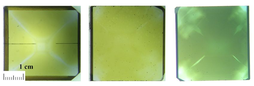
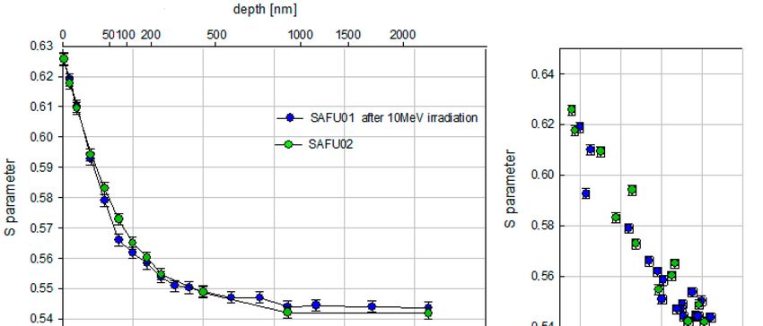
5. Results and Discussions
 Pictures of reference sample SAFU02, sample SAFU01 after electron irradiation (10
 MeV, 1 × 10¹⁶/cm2) and sample SAFU01 after electron re-irradiation (3 MeV, 1 × 10¹⁸/cm2)
Materials 2023, 16, 203 are shown in Figure 5. The sample SAFU01 changed colors after electron irradiation 6 of (3
 10
 MeV, 1 × 10¹⁸/cm2).

 Figure 5. Picture of the samples ((left)—reference sample SAFU02, (middle)—sample SAFU01 after
 Figure 5. Picture of the samples ((left)—reference sample SAFU02, (middle)—sample SAFU01 after
 electron irradiation
 electron irradiation (10
 (10 MeV, 101616
 MeV, 11 ××10 /cm/cm 2 ), (right)—sample SAFU01 after electron irradiation
 2), (right)—sample SAFU01 after electron irradiation (3
 (3 MeV, ×181018 2
 MeV, 1 ×110 /cm/cm
 2)). )).

 The results
 The resultsofofIRIRspectroscopy
 spectroscopy after
 after and
 and before
 before irradiation
 irradiation are are shown
 shown in Figure
 in Figure 6. The6.
 The samples
 samples SAFU01
 SAFU01 and SAFU02
 and SAFU02 were were
 grown grown
 underunder the same
 the same conditions,
 conditions, buthad
 but they they had
 some
 some differences in nitrogen concentration (SAFU01—220 ppm, SAFU02—198 ppm). After
 differences in nitrogen concentration (SAFU01—220 ppm, SAFU02—198 ppm). After elec-
 electron irradiation (3 MeV, 1 × 10¹⁸ /cm2 ), the nitrogen concentration in the sample
 tron irradiation (3 MeV, 1 × 10¹⁸/cm2), the nitrogen concentration in the sample SAFU01
 Materials 2023, 16, x FOR PEER
 SAFU01 REVIEW from 220 ppm to 200 ppm. The concentration of neutral vacancies was
 decreased 7 of
 decreased from 220 ppm to 200 ppm. The concentration of neutral vacancies was 5.2 ppm,
 5.2 ppm, and the concentration of negative vacancies was 20 ppm.
 and the concentration of negative vacancies was 20 ppm.

 Figure 6. Results ofFigure 6. Results of
 IR-Spectroscopy IR-Spectroscopy
 ((left ((left
 column)—before column)—before
 irradiation, irradiation, (right
 (right column)—after column)—after ir
 irradiation).
 diation).
 For Positron Annihilation Spectroscopy, diamond plates were placed at the outlet
 of the positron beamFor Positron
 from Annihilation
 the accelerator forSpectroscopy, diamond plates
 Doppler spectroscopy. Thewere placed
 samples at the outlet
 were
 irradiated with positrons having energies from 0.1 keV to 26 keV. The maximum penetration were ir
 the positron beam from the accelerator for Doppler spectroscopy. The samples
 diatedbeam
 depth of the positron with positrons having energies
 into the diamond from
 plate was 2.40.1
 µm.keV to total
 The 26 keV. The
 sum of maximum
 counts for penetrati
 depth of the positron beam into the diamond plate was 2.4 µm. The total sum of cou
 each energy was 250,000. The results of Doppler Broadening after first electron irradiation
 for each energy was 250,000. The results of Doppler Broadening after first electron irra
 (10 MeV, 1 × 10¹⁶ /cm2 ) are shown16in Figure 7. The results of Doppler Broadening after
 ation (10 MeV, 1 × 10 /cm2) are shown in Figure 7. The results of Doppler Broadening af
 second electron irradiation (3 MeV, 1 × 10¹⁸ /cm2 ) are shown in Figure 8.
 second electron irradiation (3 MeV, 1 × 10¹⁸/cm2) are shown in Figure 8.
the positron beam from the accelerator for Doppler spectroscopy. The samples were irra-
 diated with positrons having energies from 0.1 keV to 26 keV. The maximum penetration
 depth of the positron beam into the diamond plate was 2.4 µm. The total sum of counts
 for each energy was 250,000. The results of Doppler Broadening after first electron irradi-
 Materials 2023, 16, 203 7 of 10
 ation (10 MeV, 1 × 10¹⁶/cm2) are shown in Figure 7. The results of Doppler Broadening after
 second electron irradiation (3 MeV, 1 × 10¹⁸/cm2) are shown in Figure 8.

Materials 2023, 16, x FOR PEER REVIEW 8 of 10

 Figure 7. Results Figure
 of Doppler spectroscopy
 7. Results of Dopplerafter electron after
 spectroscopy irradiation
 electron(10 MeV, 1 (10
 irradiation × 10MeV,
 16/cm ). 1016 /cm2 ).
 12×

 Figure 8. Results
 Figure ofofDoppler
 8. Results Dopplerspectroscopy afterelectron
 spectroscopy after electron irradiation
 irradiation (3 MeV,
 (3 MeV, 1 18
 1 × 10 × /cm 2 ). 2).
 1018/cm

 TheThe resultofofthe
 result theDoppler
 Doppler spectroscopy
 spectroscopywas wasthe thedetermination
 determination of the
 of dependence
 the dependence of of
 parameter S in the sample on the positron energy. Figure 7 shows that the reference sample
 parameter S in the sample on the positron energy. Figure 7 shows that16the reference sam-
 SAFU02 and the sample SAFU01 after electron irradiation (10 MeV, 1 × 10 /cm2 ) do not
 plehave
 SAFU02 and thedifference
 a significant sample SAFU01
 in defects.after electron
 However, irradiation
 they (10 MeV,The
 are not identical. 1 ×decrease
 1016/cm2) do
 notofhave a significantfor
 the S-parameter difference in defects.
 energies before 10 keV However,
 is caused they are not identical.
 by thermalized The
 positrons, decrease
 which
 of the S-parameter
 diffuse back to thefor energies
 surface wherebefore 10 keV iswith
 they annihilate caused by thermalized
 a higher positrons,
 S-parameter than those inwhich
 diffuse backAbove
 the bulk. to thepositron
 surfaceimplantation
 where theyenergies
 annihilate
 of 12with
 keV, athe
 higher S-parameter
 S-parameter takes a than those in
 constant
 value. This means that almost all positrons annihilate in the bulk without
 the bulk. Above positron implantation energies of 12 keV, the S-parameter takes a con- diffusing back
 to the
 stant surface.
 value. The SWthat
 This means plotalmost
 in Figure 7 does notannihilate
 all positrons show the in presence of without
 the bulk new types of
 diffusing
 defects. An analysis of the Doppler plots of the annihilation line broadening
 back to the surface. The SW plot in Figure 7 does not show the presence of new types in Figure 8 of
 showed that the appearance of defects in the sample SAFU01 occurred after electron re-
 defects. An analysis of the18Doppler plots of the annihilation line broadening in Figure 8
 irradiation (3 MeV, 1 × 10 /cm2 ). In the near-surface layer, the differences between the
 showed that the appearance of defects in the sample SAFU01 occurred after electron re-
 sample SAFU01 before and after irradiation (3 MeV, 1 × 10¹⁸ /cm2 ) start at a positron
 irradiation (3 MeV, 1 × 10¹⁸/cm2). In the near-surface layer, the differences between the
 sample SAFU01 before and after irradiation (3 MeV, 1 × 10¹⁸/cm2) start at a positron energy
 of 2 keV. This roughly corresponds to 20 nm. The S parameter then decreases with in-
 creasing positron energy. Above positron implantation energies of 6 keV, the S-parameter
 takes a constant value. There are significant differences between the samples starting from

Materials 2023, 16, 203 8 of 10

 energy of 2 keV. This roughly corresponds to 20 nm. The S parameter then decreases with
 increasing positron energy. Above positron implantation energies of 6 keV, the S-parameter
 takes a constant value. There are significant differences between the samples starting
 from a depth of about 200 nm. The SW plot in Figure 8 shows the appearance of a new
 type of defect in the sample SAFU01 after irradiation (3 MeV, 1 × 10¹⁸ /cm2 ). From a
 comparison of Figures 7 and 8, it can be observed that the area where almost all positrons
 annihilate in the bulk without diffusing back to the surface shift from 380 nm to 170 nm.
 Irradiation by electrons (3 MeV, 1 × 10¹⁸ /cm2 ) created a significant increase in defects in a
 synthetic diamond plate at depths of up to 2.4 µm in contrast to irradiation by electrons
 with other parameters (10 MeV, 1 × 10¹⁶ /cm2 ), which did not create defects in a sample at
 the same depths.
 In addition, the positron diffusion length was determined using the VEPFIT pro-
 gram [31]. A one-layer model was used for determining the positron diffusion length.
 The positron diffusion length of the SAFU01 sample before irradiation was 83.3 nm. After
 electron irradiation (3 MeV, 1 × 10¹⁸ /cm2 ), the positron diffusion length of the SAFU01
 sample was 67.9 nm. The positron diffusion length decreases after electron irradiation
 (3 MeV, 1 × 10¹⁸ /cm2 ), which represents an increased number of defects below the surface.

 6. Conclusions
 In summary, the investigation has shown that the irradiation of a synthetic diamond
 plate by electrons (10 MeV, 1 × 10¹⁶ /cm2 ) is not enough for formation vacancy, and at
 NV-centers at depths of up to 2.4 µm, such electron irradiation practically does not in-
 fluence vacancy defects formation at the same depths. The electron irradiation (3 MeV,
 1 × 10¹⁸ /cm2 ) causes the formation of vacancies in the sample, which is shown by both
 infrared spectroscopy and positron annihilation spectroscopy, with significant vacancy
 formation concentrated at depths from 200 nm to 2400 nm. IR spectroscopy has shown
 that, after irradiation, the nitrogen concentration in the sample decreased (from 220 ppm to
 200 ppm) and defects have appeared (neutral vacancies—5.2 ppm and negative vacancies—
 20 ppm). Distribution maps of IR spectroscopy showed the nature of the nitrogen defect
 distribution. After irradiation, the distribution map of single-nitrogen defect distribution
 became blurred. It is shown that positron annihilation spectroscopy is a sensitive method of
 detecting defects in samples of diamond plates and can be used alongside other optical re-
 search methods, such as infrared spectroscopy, as a method of detecting defect distribution
 over the depth of diamond plates.

 Author Contributions: Conceptualization, M.E. and I.M.; methodology, I.K.; experiments using
 method PAS, I.K., A.S. and O.O.; experiments using method IR-spectroscopy, A.K.; validation, M.E.
 and I.M.; formal analysis, M.E. and I.M.; writing—original draft preparation, I.K. and A.K.; writing—
 review and editing, I.K., A.K. and M.E.; project administration, M.E. All authors have read and agreed
 to the published version of the manuscript.
 Funding: The research was supported by of the state assignment of the Russian Federation No.
 0793-2020-0005 and No. FSRU 2021-0008.
 Institutional Review Board Statement: Not applicable.
 Informed Consent Statement: Not applicable.
 Data Availability Statement: Not applicable.
 Acknowledgments: We thank Andrey Anisimov and Victor Wiens for providing samples for research
 and their post-growth processing.
 Conflicts of Interest: The authors declare no conflict of interest.

Materials 2023, 16, 203 9 of 10

References
1. Hybertsen, M.S.; Louie, S.G. Electron correlation in semiconductors and insulators: Band gaps and quasiparticle energies. Phys.
 Rev. B 1986, 34, 5390–5413. [CrossRef] [PubMed]
2. Rondin, L.; Tetienne, J.-P.; Hingant, T.; Roch, J.-F.; Maletinsky, P.; Jacques, V. Magnetometry with nitrogen-vacancy defects in
 diamond. Rep. Prog. Phys. 2014, 77, 056503. [CrossRef] [PubMed]
3. Balasubramanian, G.; Neumann, P.; Twitchen, D.; Markham, M.; Kolesov, R.; Mizuochi, N.; Isoya, J.; Achard, J.; Beck, J.; Tissler, J.;
 et al. Ultralong spin coherence time in isotopically engineered diamond. Nat. Mater. 2009, 8, 373–377. [CrossRef] [PubMed]
4. Chen, Y.-Y.; Shu, H.; Kuo, Y.; Tzeng, Y.-K.; Chang, H.-C. Measuring Forster resonance energy transfer between fluorescent
 nanodiamonds and near-infrared dyes by acceptor photobleaching. Diam. Relat. Mater. 2011, 20, 803–807. [CrossRef]
5. Maze, J.R.; Stanwix, P.L.; Hodges, J.S.; Hong, S.; Taylor, J.M.; Cappellaro, P.; Jiang, L.; Gurudev Dutt, M.V.; Togan, E.; Zibrov, A.S.;
 et al. Nanoscale magnetic sensing with an individual electronic spin in diamond. Nature 2008, 455, 644–647. [CrossRef]
6. Greentree, A.D.; Fairchild, B.A.; Hossain, F.M.; Prawer, S. Diamond integrated quantum photonics. Mater. Today 2008, 11, 22–31.
 [CrossRef]
7. Waldermann, F.C.; Olivero, P.; Nunn, J.; Surmacz, K.; Wang, Z.Y.; Jaksch, D.; Taylor, R.A.; Walmsley, I.A.; Draganski, M.; Reichart,
 P.; et al. Creating diamond color centers for quantum optical applications. Diam. Relat. Mater. 2007, 16, 1887–1895. [CrossRef]
8. Markham, M.L.; Dodson, J.M.; Scarsbrook, G.A.; Twitchen, D.J.; Balasubramanian, G.; Jelezko, F.; Wrachtrup, J. CVD diamond for
 spintronics. Diam. Relat. Mater. 2011, 20, 134–139. [CrossRef]
9. Du Preez, L. Electron Paramagnetic Resonance and Optical Investigations of Defect Centres in Diamond. Ph.D. Thesis, University
 of the Witwatersrand, Johannesburg, South Africa, 1965.
10. Davies, G.; Hamer, M.F. Optical studies of the 1.945 eV vibronic band in diamond. Proc. Royal Soc. A 1976, 348, 285–298. [CrossRef]
11. Gruber, A.; Dräbenstedt, A.; Tietz, C.; Fleury, L.; Wrachtrup, J.; von Borczyskowski, C. Scanning confocal optical microscopy and
 magnetic resonance on single defect centers. Science 1997, 276, 2012–2014. [CrossRef]
12. Dräbenstedt, A.; Fleury, L.; Tietz, C.; Jelezko, F.; Kilin, S.; Nizovtzev, A.; Wrachtrup, J. Low-temperature microscopy and
 spectroscopy on single defect centers in diamond. Phys. Rev. B 1999, 60, 503–508. [CrossRef]
13. Brouri, R.; Beveratos, A.; Poizat, J.-P.; Grangier, P. Photon antibunching in the fluorescence of individual color centers in diamond.
 Opt. Lett. 2000, 25, 1294–1296. [CrossRef]
14. Jelezko, F.; Gaebel, T.; Popa, I.; Domhan, M.; Gruber, A.; Wrachtrup, J. Observation of Coherent Oscillation of a Single Nuclear
 Spin and Realization of a Two-Qubit Conditional Quantum Gate. Phys. Rev. Lett. 2004, 93, 130501. [CrossRef] [PubMed]
15. Jelezko, F.; Gaebel, T.; Popa, I.; Gruber, A.; Wrachtrup, J. Observation of Coherent Oscillations in a Single Electron Spin. Phys. Rev.
 Lett. 2004, 92, 076401. [CrossRef] [PubMed]
16. Positron Annihilation Spectroscopy at the HZDR. Available online: https://www.hzdr.de/db/Cms?pNid=3581 (accessed on
 15 November 2022).
17. Schultz, P.J.; Lynn, K.G. Interaction of positron beams with surfaces, thin films, and interfaces. Rev. Mod. Phys. 1988, 60, 701–779.
 [CrossRef]
18. Pu, A.; Bretagnon, T.; Kerr, D.; Dannefaer, S. Positron annihilation investigation of vacancies in as-grown and electron-irradiated
 diamonds. Diam. Relat. Mater. 2000, 9, 1450–1463. [CrossRef]
19. Procházka, I. Positron annihilation spectroscopy in materials structure studies. Mater. Struct. 2001, 8, 55–60.
20. Tuomisto, F.; Makkonen, I. Defect identification in semiconductors with positron annihilation: Experiment and theory. Rev. Mod.
 Phys. 2013, 85, 1583–1631. [CrossRef]
21. Sidorin, A.A.; Meshkov, I.; Ahmanova, E.; Eseev, M.; Kobets, A.; Lokhmatov, V.; Pavlov, V.; Rudakov, A.; Yakovenko, S. The
 LEPTA Facility for Fundamental Studies of Positronium Physics and Positron Spectroscopy. Mater. Sci. Forum 2013, 733, 291–296.
 [CrossRef]
22. Horodek, P.; Eseev, M.K.; Kobets, A.G. Studies of stainless steel exposed to sandblasting. Nukleonika 2015, 60, 721–724. [CrossRef]
23. Siemek, K.; Eseev, M.K.; Horodek, P.; Kobets, A.G.; Kuziv, I.V. Defects studies of nickel aluminum bronze subjected to cavitation.
 Appl. Surf. Sci. 2021, 546, 149107. [CrossRef]
24. Fischer, C.G.; Connell, S.H.; Coleman, P.G.; Malik, F.; Britton, D.T.; Sellschop, J.P.F. A slow positron beam study of natural and
 synthetic diamonds. Appl. Surf. Sci. 1999, 149, 221–226. [CrossRef]
25. Uedono, A.; Fujii, S.; Morishita, N.; Itoh, H.; Tanigawa, S.; Shikata, S. Defects in synthesized and natural diamond probed by
 positron annihilation. J. Phys. Condens. Matter 1999, 11, 4109–4122. [CrossRef]
26. Jerzy Dryzek Homepage. Available online: https://ifj.edu.pl/private/jdryzek/page_r18.html (accessed on 15 November 2022).
27. Kiflawi, I.; Mayer, A.E.; Spear, P.M.; Van Wyk, J.A.; Woods, G.S. Infrared absorption by the single nitrogen and A defect centres in
 diamond. Philos. Mag. B 1994, 69, 1141–1147. [CrossRef]
28. Boyd, S.R.; Kiflawi, I.; Woods, G.S. The relationship between infrared absorption and the A defect concentration in diamond.
 Philos. Mag. B 1994, 69, 1149–1153. [CrossRef]
29. Malogolovets, V.G. Studying the Impurity Composition and Real Structure of Synthetic DIAMONDS by Spectroscopic Methods.
 Ph.D. Thesis, IPM Academy of Sciences, Kiev, Ukraine, 1979.
Materials 2023, 16, 203 10 of 10

30. Lawson, S.C.; Fisher, D.; Hunt, D.C.; Newton, M.E.J. On the existence of positively charged single-substitutional nitrogen in
 diamond. J. Phys. Condens. Matter 1998, 10, 6171. [CrossRef]
31. Van Veen, A.; Schut, H.; Clement, M.; de Nijs, J.M.M.; Kruseman, A.; Ijpma, M.R. VEPFIT applied to depth profiling problems.
 Appl. Surf. Sci. 1995, 85, 216–224. [CrossRef]

Disclaimer/Publisher’s Note: The statements, opinions and data contained in all publications are solely those of the individual
author(s) and contributor(s) and not of MDPI and/or the editor(s). MDPI and/or the editor(s) disclaim responsibility for any injury to
people or property resulting from any ideas, methods, instructions or products referred to in the content.
You can also read