LIGHT HARVESTING IN LARGE-AREA NANOSTRUCTURED 2D-MOS 2 LAYERS - MATTEO GARDELLA UNIVERSITÀ DI GENOVA - DIPARTIMENTO DI FISICA JOINT EPS-SIF ...
←
→
Page content transcription
If your browser does not render page correctly, please read the page content below
Light harvesting in large-area
nanostructured 2D-MoS2 layers
 Matteo Gardella
 Università di Genova - Dipartimento di Fisica
 Joint EPS-SIF International School on Energy 2021
 Tuesday, July 20th

Why this talk?
Evolution of solar cells:
1° generation → silicon (p-n junctions)
2° generation → thin films
3° generation → new concepts (e.g. nanostructured solar cells)

➢ 2D-semiconductors (like MoS2) represent ultimate thin films
➢ Efficient light harvesting is required for increasing optical absorption
➢ Absorption enhancement is only a first step towards competitive
 performances for solar cells (other challenges to be faced: e.g. high
 quality material growth, electrical performances)
Transition Metal Dichalcogenides (TMDCs)
 2D materials portfolio

 Jariwala et al., ACS Photonics 2017,
 4, 2962−2970
 TMDCs promising materials
 for opto-electronics and
MoS2 bandgap energy between 1,2eV and 1,9eV photovoltaics!
Fabrication routes
Mechanical exfoliation Large area growth
 e.g. Chemical Vapor Deposition

 ▪ crystalline quality ▪ large area
 ▪ good electronic properties ▪ scalable
 ▪ small area ▪ conformal growth
 ▪ randomic process ▪ polycristalline
 2μm ▪ expensive lithography ▪ lower properties
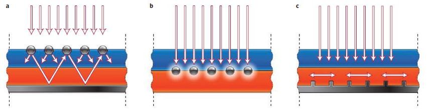
Light harvesting strategies
 Despite the MoS2 high optical absorption coefficient, the atomical thickness reduces
 the effective absorption requiring light harvesting strategies
 Plasmonic coupling Diffractive anomalies

 Light deviated parallel to the
 active 2D material surface

 Rayleigh Anomaly
 Guided Mode Anomaly
Atwater, Polman, Nature Mater 9, 205–213 (2010) (launched by the grating) q
 ➢ Light scattering
 = ⋅ + θ
 ➢ Back-reflection
 ➢ Localized surface plasmons E H
 ➢ Surface plasmon polaritons
 Bhatnagar et al., Nanoscale, 2020, 12, 24385–24393
 Bhatnagar et al., ACS Appl. Mater. Interfaces 2021, 13, 13508-13516
Large area 2
 (cm ) gratings fabrication
 Photoresist
 SiO2 λ
 P=
 2 sin θ
 Laser Interference
 Lithography (LIL)
 Lloyd’s mirror LIL configuration
Polymer mask
 1
 1. MoS2 nanostripes arrays
 MoS2 deposition

2 Al deposition
 2. Continuous MoS2 films
 Metal mask Reactive Ion SiO2 grating
 on silica grating
 Etching MoS2 deposition
MoS2 nanostripes arrays
Growth of 4nm thick MoS2 stripes Diffractive anomaly
 (different stripes width)
 MoS2
 SiO2

 Normalizing to the MoS2 surface
 coverage, higher extinction with less
 material comparing to continuous
 flat MoS2 film!

 Bhatnagar et al., Nanoscale, 2020, 12, 24385–24393

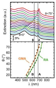
Continuous MoS2 films on silica gratings Diffractive anomaly Conformal growth of 4nm MoS2 layers on top of silica gratings q (°) 60 = ⋅ + θ 55 MoS2 Extinction (a.u.) 50 45 SiO2 40 700 A 35 30 25 600 B (nm) 20 Sample 2 (P=450nm) 15 10 Sample 1 (P=290nm) 5 500 0,25 0 C 60 D C B A 400 D 50 RAair 40 300 200 0 5 10 15 20 25 30 35 q (°) q() 30 z (nm) 100 P=290nm 20 Tunability in a broad spectral range 10 RAsub (300-700nm) by controlling either GMA 0 0 250 500 750 300 400 500 600 700 800 900 the period or the incidence angle x (nm) (nm) Bhatnagar et al., ACS Appl. Mater. Interfaces 2021, 13, 13508-13516

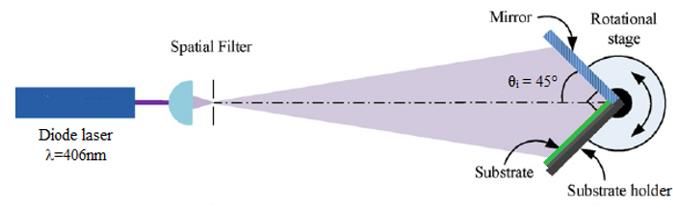
Total integrated transmission measurements 0,4 0,4 Flat MoS2 Sample 1 0,3 0,3 q=0° q=0° q=35° q=35° Absorption Absorption 0,2 q=40° 0,2 q=40° q=45° q=45° 0,1 0,1 0,0 0,0 500 600 700 800 900 500 600 700 800 900 Integrating sphere setup (nm) (nm) Detected signal (S): integrated ✓ Resonant absorption enhancement up to 240% at θ=45° transmission, reflection and ✓ Averaged absorption gain (470-750nm) ≈110% at θ=45° diffuse scattering Absorption: A=1-S Bhatnagar et al., ACS Appl. Mater. Interfaces 2021, 13, 13508-13516
Conclusions
➢ Scalable fabrication of large area nanostructured samples (either MoS2 stripes
 arrays or conformal MoS2 layers on silica gratings)
➢ Tunable and broadband absorption enhancement in MoS2 ultra-thin films via
 diffractive anomalies

 Co-authors acknowledgements
F Buatier de Mongeota, MC Giordanoa, M Bhatnagara, D Chowdhurya, C Mennuccia,
 A Mazzantib, G Della Valleb, C Martellac, P Tummalac, A Lampertic, A Mollec
 (a) Dipartimento di Fisica, Università di Genova, Via Dodecaneso 33, 16146 Genova, Italy
(b) Dipartimento di Fisica and IFN-CNR, Politecnico di Milano, Piazza Leonardo da Vinci, 32 - 20133 Milano, Italy
 (c) CNR-IMM Unit of Agrate Brianza, via C. Olivetti 2, Agrate Brianza, I-20864, Italy
You can also read