PROBING OF NEGATIVELY CHARGED AND NEUTRAL EXCITONS IN MONOLAYER MOS2
←
→
Page content transcription
If your browser does not render page correctly, please read the page content below
Probing of negatively charged and neutral excitons
                                                     in monolayer MoS2
arXiv:2001.07929v2 [cond-mat.mes-hall] 23 Mar 2020

                                                                  J Jadczak1 , J Kutrowska-Girzycka1 , M Bieniek2,3 , T
                                                                  Kazimierczuk4 , P Kossacki4 , J J Schindler5 , J Debus5 , K
                                                                  Watanabe6 , T Taniguchi6 , C H Ho7 , A Wójs2 , P Hawrylak3
                                                                  and L Bryja1
                                                                  1
                                                                    Department of Experimental Physics, Wroclaw University of Science and
                                                                  Technology, Wybrzeże Wyspiańskiego 27, 50-370 Wroclaw, Poland
                                                                  2
                                                                    Department of Theoretical Physics, Wroclaw University of Science and Technology,
                                                                  Wybrzeże Wyspiańskiego 27, 50-370 Wroclaw, Poland
                                                                  3
                                                                    Department of Physics, University of Ottawa, Ottawa, Ontario, Canada K1N 6N5
                                                                  4
                                                                    Institute of Experimental Physics, Faculty of Physics, University of Warsaw,
                                                                  Pasteura 5, 02-093 Warsaw, Poland
                                                                  5
                                                                    Experimentelle Physik 2, Technische Universitt Dortmund, 44227 Dortmund,
                                                                  Germany
                                                                  6
                                                                    National Institute for Materials Science, Tsukuba, Ibaraki, 305-0044, Japan
                                                                  7
                                                                    Department of Electronic Engineering, National Taiwan University of Science and
                                                                  Technology, Taipei, 106, Taiwan
                                                                  E-mail: joanna.jadczak@pwr.edu.pl

                                                                  March 2020

                                                                  Abstract. We present results of optical experiments and theoretical analysis on the
                                                                  high-quality single-layer MoS2 which reveal the fine structure of charged excitons, i.e.,
                                                                  trions. In the emission spectra we resolve and identify two trion peaks, T1 and T2 ,
                                                                  resembling the pair of singlet and triplet trion peaks (TS and TT ) in tungsten-based
                                                                  materials. However, in polarization-dependent photoluminescence measurements we
                                                                  identify these peaks as intra- and inter-valley singlet trions due to the trion fine
                                                                  structure distinct from that already known in bright and dark 2D materials with
                                                                  large conduction-band splitting induced by the spin-orbit coupling. We show that
                                                                  the trion energy splitting in MoS2 is a sensitive probe of inter- and intra-valley carrier
                                                                  interaction. With additional support from theory we claim that the existence of these
                                                                  singlet trions combined with an anomalous excitonic g-factor together suggest that
                                                                  monolayer MoS2 has a dark excitonic ground state, despite having ”bright” single-
                                                                  particle arrangement of spin-polarized conduction bands.

                                                     Keywords: transition metal dichalcogenides monolayers, molybdenum disulfide, exciton,
                                                     trion, Zeeman g-factor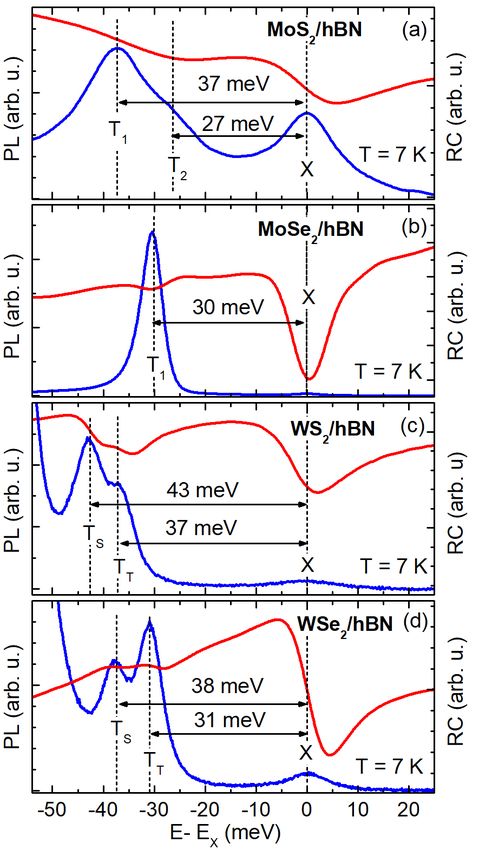
Probing of negatively charged and neutral excitons in monolayer MoS2                       2

1. Introduction

Monolayer transition metal dichalcogenides (TMDs) have attracted considerable
scientific interest due to their unique physical properties [1, 2, 3], such as direct optical
bandgaps located at ±K valleys of two dimensional (2D) hexagonal Brillouin zone [4]
and coupling of spin and valley degrees of freedom [5]. Their 2D nature and reduced
dielectric screening enable formation of excitons with binding energies of few hundreds
of meV [6], orders of magnitude larger than those in typical quasi-2D quantum wells
[7, 8]. In addition to neutral excitons, in the presence of excess carriers, also trions can
be formed [9, 10, 11, 12, 13, 14] with binding energies (EB ) of tens of meV, resulting
in their stability even at room temperatures [15, 16, 17]. Consequently, the monolayer
TMDs constitute a novel platform to optically probe many-body effects in the presence
of strong Coulomb interactions [11, 18, 19, 20, 21, 22], particularly when the Fermi level
in the conduction band for n-doped samples is lower or of the same order as the trion
binding energy [23, 24, 25].
     Monolayer MoS2 is probably the best-known member of semiconducting TMDs
[26] due to its natural abundance in almost chemically pure mineral molybdenite [27].
Compared to other materials from the MX2 (M = Mo, W; X = S, Se, Te) family,
MoS2 is unique having a small spin splitting (∼ 3 meV) of the conduction band [28],
in comparison to typical Fermi energies in n-type exfoliated TMDs monolayers (ML)
transferred onto standard SiO2 /Si substrate [3, 29]. Until recently, the optical quality of
monolayer MoS2 was inferior in quality to the related materials, such as MoSe2 , WS2 , and
WSe2 . This allowed for observation of only broad photoluminescence peaks dominated
by trions [15]. However, progress was made by encapsulation of a MoS2 monolayer with
hexagonal boron nitride (hBN) layers, resulting in narrow neutral exciton lines with a
width of about 2 meV at low temperatures (4 K) [30]. The high-quality MoS2 /hBN
van der Waals heterostructures hence enabled the observation of subtle optical and
spin-valley properties of monolayer MoS2 [30, 31, 25].
     Recent works reported of a trion emission line splitting in the presence of carriers
in gated nanostructures [25], similar to other ”dark” TMDs [32]. Within a trion model,
inter- and intra- valley singlet and triplet trion nature of these split lines was suggested
[23], with a splitting energy of about 5 meV. Contrary to those calculations, triplet
trion in MoS2 was shown to be unbound in reference [33], predicting intra-/inter- valley
singlet-singlet splitting ∼ 4 meV. Interestingly, small values of an effective exciton g-
factor in hBN encapsulated MoS2 monolayers, g = −1.7 in magneto-photoluminescence
experiments [30] and g = −3.0 in magneto-transmission measurements [31], have also
been observed. Furthermore, detailed magneto-transmission experiments have revealed
that the reduced mass of the exciton in monolayer MoS2 is heavier than predicted
by density functional theories [28, 34], suggesting a large electron mass consistent
with recent values determined from transport studies of n-type MoS2 monolayers [35].
The complicated interplay of band structure [28, 36], electron-electron interactions
[11, 24, 37, 38], enhanced spin-splitting [39], dynamical effects [40] and inter-/ intra-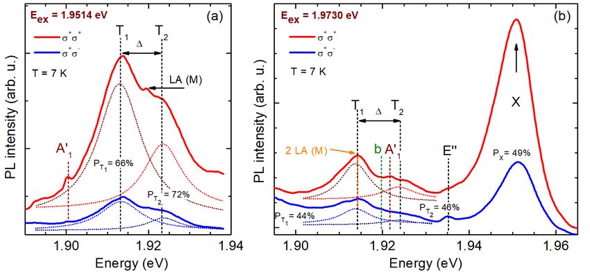
Probing of negatively charged and neutral excitons in monolayer MoS2                       3

valley phonon [41] and plasmon [20] contributions makes MoS2 one of the most
challenging materials to understand.

              Figure 1. The comparative PL and RC spectra for (a) MoS2 /hBN, (b) MoSe2 /hBN,
              (c) WS2 /hBN, (d) WSe2 /hBN structures measured at 7 K.

2. PL and RC measurements of MX2

As a first step toward this understanding we present results of photoluminescence (PL)
and reflectance contrast (RC) measurements of Mo- and W-based monolayer TMDs.
Figure 1(a-d) compares low temperature (7 K) PL and RC spectra of molybdenum
and tungsten based TMDs monolayers deposited on hBN/SiO2 /Si substrate. The PL
spectra are excited non-resonantly at an energy of 2.33 eV. For all monolayers, the
optical transitions are associated with the nearly free states of the neutral exciton (X)
[16] and different types of trions (T1 , T2 , TS , TT ) [42, 43]. In all spectra the energies
are measured from exciton energy. In figure 1(a) we show PL and RC spectra for MoS2
while figure 1(b) shows the same spectra for MoSe2 . Interestingly, in the PL spectrum
of MoS2 we see an exciton peak X and two, T1 and T2 , peaks at lower energy. As
indicated in figure 1(a) the energy separation between these optical trion transitions is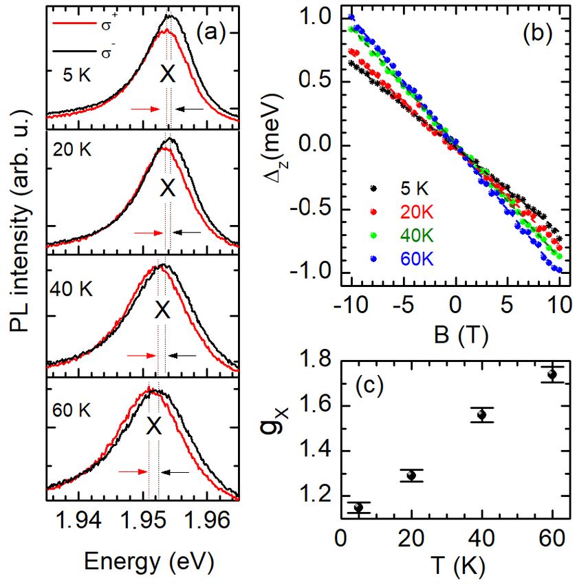
Probing of negatively charged and neutral excitons in monolayer MoS2                                 4

∆ ≈ 10 meV. We attribute them tentatively to the recombination from trion states.
The MoS2 spectra are to be contrasted with the spectra of MoSe2 , see figure 1(b),
which demonstrate an exciton and only a single trion T1 line. However, the doublet
structure of the trion emission line positioned below the neutral exciton in MoS2 is
similar to the trion emission spectra in tungsten based monolayers, shown in figure 1(c-
d). In the PL and RC spectra of WS2 (figure 1(c)) and WSe2 (figure 1(d)), the TS
and TT optical transitions are identified at low doping level (EF
Probing of negatively charged and neutral excitons in monolayer MoS2 5
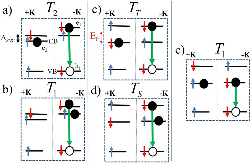
electron states is inverted and the lowest energy state is dark. We now explain [45] this
bright-dark ground excitonic state inversion shown in figure 2(a). The first mechanism
is related to different masses of spin-up and -down electrons in the conduction band.
The higher energy spin-up conduction band in the −K valley is heavier; hence the
higher electron mass combined with electron-hole attraction results in a more strongly
bound dark state, pushing the electron-hole bright configuration up in energy. The
second contribution adding to the blue shift of the energy of the bright configuration
is the repulsive electron-hole exchange interaction. The two effects result in a splitting
of the bright-dark 1s excitons up to 9 meV. Figure 2(b) shows the configuration of the
intra-valley trion where two electrons in the CB are in the same −K valley and hence
necessarily in the singlet state. Accordingly, both trions T1 and T2 are bright singlet
trions and the lowest energy trion is dark.
The unusual arrangement of the trion states in a material with a positive and
small spin-orbit induced splitting of the conduction band is contrary to trion states in
materials with a negative and large spin-orbit induced splitting of the conduction band
such as WS2 and WSe2 , see figure 2(c,d). The single particle arrangement of levels
in the +K valley, left panel in figure 2(c,d) is opposite to the level arrangement in
figure 2(a,b). There is no inversion of electronic levels for the electron in the presence
of valence hole in the −K valley. Hence, the TT trion is a triplet and the lowest
energy inter-valley trion is dark. The TS trion is a singlet trion, as the T1 line in
MoS2 . The observation of the doublet structure of bright high-energy trions (TS , TT )
in WSe2 and WS2 monolayers results from the fact that in tungsten based monolayers
the optically active exciton (X) is associated with the top spin-split valence subband
(VB) and the upper spin-split conduction band subband (CB). Hence, for low two-
dimensional electron gas concentration, as the electron Fermi level is positioned between
the spin-split conduction bands, the triplet trion (figure 2(c)) comprises two electrons
from different valleys [46], whereas the singlet trion must involve two electrons from
the same valley (figure 2(d)). Additionally, in the simplest case of only one charged
complex, the T1 trion in MoSe2 (figure 1(b)) is formed from the optically active exciton
(X) associated with the top spin-split valence band (VB) subband and the lower spin-
split conduction band (CB) subband, see figure 2(e). Accordingly, for the low 2DEG
concentration and Fermi level positioned close to the lower spin-split conduction band,
the singlet trion should involve two electrons from the different valleys forming the
inter-valley spin singlet trion (TS ) with two electrons located in the lower conduction
bands.
The assignment of T2 (figure 2(a)) and T1 (figure 2(b)) emission features in MoS2
to the inter-valley and intra-valley bright singlet trions instead of singlet-triplet trions is
related to the relatively small, compared with WS2 or WSe2 monolayers, spin-splitting
and Fermi level position in the conduction band. We note that the inter-valley triplet
trion in such band arrangement is not only less probable due to Fermi level position,
but was also predicted to be unbound due to exchange interaction [33].Probing of negatively charged and neutral excitons in monolayer MoS2 6
Figure 3. (a) The polarization-resolved PL spectra of MoS2 excited strictly resonantly
at the neutral exciton energy of 1.9514 eV. (b) The resonant circularly-polarized PL
00 0
spectra for 1.9730 eV excitation, revealing E , A1 , b and 2LA (M ) Raman features.
4. Polarization-resolved PL excitation of trions in monolayer MoS2
To firmly establish the singlet nature of the T1 and T2 transitions observed in the PL
spectra of monolayer MoS2 , we perform polarization-resolved and excitation energy-
dependent PL measurements at T = 7 K. Figure 3 shows the examples of polarization-
resolved PL spectra excited strictly resonantly at the neutral exciton energy of 1.9514 eV
(figure 3(a)) and near-resonantly at the energy of 1.9730 eV (figure 3(b)). We observe
also the Raman features, which shift as a function of the excitation energy and are
0 0
attributed to first- and second-order scattering processes, such as A1 , E modes and b,
2LA (M ) or LA (M ) bands, respectively [47, 48]. The presence of the LA(M ) band in
the Raman scattering spectrum is likely due to defects or disorder in the sample which
localize phonons [47]. Furthermore, we analyze the optical orientation of trions, i.e. the
helicity of the outgoing light with respect to the helicity of their emission. Based on
the fitting of the trion contributions to the PL spectrum excited at the neutral exciton
energy X (figure 3(a)) with a combination of two Lorentzian curves, we determine the
degree of helicity preservation of the emitted light with respect to exciting light defined
as P = (Iσ+ σ+ − Iσ+ σ− )/(Iσ+ σ+ + Iσ+ σ− ) for each trion component, where σ + σ + and
σ + σ − indicate the co-circular and cross-circular configurations, respectively. The T1
line displays the PT1 value of almost 66%, while the T2 line has a slightly higher PT2 of
about 72%. For the excitation energy equal to 1.9730 eV (slightly higher than the X
energy) we obtain P values of 44%, 46% and 49% for T1 , T2 and X, respectively (figure
3(b)). In monolayer TMDs, the large exciton valley polarization obtained in the steady-
state PL experiments results from the competition between the valley depolarization
time (∼ 1 ps) and the ultra-fast exciton population relaxation time (∼ 100 - 200 fs)
[49, 50]. However, the trions exhibit an extended population relaxation time of tensProbing of negatively charged and neutral excitons in monolayer MoS2 7
of picoseconds. It has been established in a recent work [51] that the most efficient
scattering mechanism responsible for the trion valley depolarization in WSe2 is due to
scattering of an electron-hole pair between valleys. This process is mediated by the
electron-hole exchange interaction towards an energetically favorable trion state. In
contrast to tungsten based TMDs, where the preservation of helicity of the excitation
light in the emission spectrum of TS and TT trions is significantly different, e.g. about
16% and 50% in steady-state PL measurements of monolayer WS2 [43], in monolayer
MoS2 both values are comparable. This supports the interpretation that both trion lines
originate from singlet states.
5. Trion splitting as a measure of correlations
Having established the singlet nature of the T1 and T2 trions, we comment on processes
determining their energy splitting. The difference in the total energy of the T1 and T2
configurations ET1 − ET2 = ∆SOC + V ∗ , can be written as a sum of conduction band spin
splitting ∆SOC and electron-electron interactions, V ∗ . V ∗ reflects a subtle imbalance
between electron-hole and electron-electron interactions inside and between valleys. A
simple analysis leads to the expression
V ∗ = V D (e1 , +K; e2 , +K) − V D (h1 , +K; e2 , +K) +
D (1)
V (e1 , +K; e2 , −K) − V D (h1 , +K; e2 , −K ,
where e1,2 (h1 ) describe electrons (hole) forming trion (see figure 2(a)) and V D is the
total direct interaction energy between particles. We see that V ∗ is the sum of two
contributions, a difference between the electron-electron repulsion and electron-hole
attraction in the same valley and between valleys. Interestingly, a similar analysis
of the singlet-triplet trion splitting in tungsten-based materials leads to ETS − ETT =
V X (e1 , +K; e2 , −K) + V ∗ . It suggests that the energy of the singlet-singlet splitting is
a new measure for electronic correlations in 2D crystals with small spin-orbit splitting
in conduction bands.
6. Zeeman g-factor in monolayer MoS2
The relative PL intensity of T1 and T2 features significantly depends on the quality of
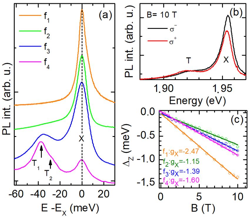
the sample and doping level. Figure 4(a) compares low temperature (7 K) PL spectra
of four different MoS2 monolayers: (i) one hBN-encapsulated (hBN/MoS2 /hBN)- f1 and
(ii) three monolayers with only down hBN substrate (MoS2 /hBN) with different hBN
thickness: f2 -100 nm, f3 -130 nm, f4 -250 nm, respectively. Similarly to our previous
studies on WS2 /hBN/SiO2 structures [22], an extra hBN layer used between the flake
and SiO2 /Si substrate acts as a buffer layer and changes the doping level in the monolayer
system. Accordingly, the presented PL spectra reveal relatively different 2D electron
gas (2DEG) concentrations, which is qualitatively estimated by the trion to exciton
emission intensity ratio (T /X) [22, 16]. At very low 2DEG concentration, foreseenProbing of negatively charged and neutral excitons in monolayer MoS2 8
for the hBN-encapsulated sample (f1 ), the X line solely dominates the PL spectrum
(Fig. 4(a), orange line), whereas both T lines are not detectable. Also, for one of
the MoS2 /hBN samples (f2 , green line), for which the neutral exciton is very intensive;
however, below its energy position the PL spectrum exhibits a dim and broad trion
shoulder. Moreover, for both the hBN-encapsulated (f1 ) and MoS2 /hBN (f2 ) samples
the linewidth (FWHM) is most narrow and reaches about 5 meV at 7 K. At a slightly
higher 2DEG concentration (sample f3 ), the emission intensity of broaden T transitions
increases. Nevertheless, the double trion structure becomes well resolved only for the
highest electron doping (f4 , magenta line), as the trion emission intensity exceeds that
of a neutral exciton. Our observations are consistent with recent results concerning an
optical susceptibility measurement of a gated MoS2 device [25].
Figure 4. (a) The comparison of low temperature (7 K) PL spectra of dierent MoS2
monolayers: hBN-encapsulated - f1 , and three MoS2 /hBN structuress with dierent
thicknesses of hBN layers: f2 -100 nm, f3 -130 nm, f4 -250 nm, respectively. (b) The
circularly-polarized PL spectrum for f3 sample at B = 10 T. (c) Exciton Zeeman
splitting.
Let us now discuss the magneto-optical response observed in the PL spectra at
T = 5 K. Figure 4(b) presents the typical, polarization-resolved PL spectrum for
MoS2 /hBN at B = 10 T (f3 ). Using non-resonant (2.331 eV) and linearly polarized
laser excitation we find that, for the applied magnetic fields and all the samples, the
trion features are not sufficiently resolved in the PL spectra to estimate their effective
g-factors. Accordingly, we focus only on the 2DEG dependence of the exciton g-factors.
In figure 4(c) we extracted the Zeeman splitting ∆Z of the neutral exciton X for all
the samples; it is defined as the shift between the σ + and σ − polarized components
of the PL: ∆Z = Eσ+ − Eσ− = gX µB B. This quantity depends linearly on the
magnetic field and our measurement suggest the exciton g-factor of gX = −1.15 ± 0.01,
gX = −1.39 ± 0.01, gX = −1.60 ± 0.01 and gX = −2.45 ± 0.01 for samples f2 , f3 , f4 and
f1 , respectively. Interestingly, for all the MoS2 /hBN structures without a cap layer the
exciton g-factor increases with rising thickness of the hBN layer: f2 -100 nm, f3 -130 nm,
f4 -250 nm, respectively. For the high-quality hBN-encapsulated monolayer MoS2 (f1 ) theProbing of negatively charged and neutral excitons in monolayer MoS2 9
exciton g-factor is the highest. Furthermore, we probed the temperature dependence of
the exciton effective g-factor in the MoS2 /hBN structure (f2 ), whose emission spectra
are dominated only by a sharp and relatively narrow X line. Figure 5(a) compares
typical PL spectra of the MoS2 /hBN structure with relatively low doping, measured
at different temperatures (5 K, 20 K, 40 K, 60 K) and a magnetic field of B = 10 T.
The exciton Zeeman splitting at four different temperatures is shown in figure 5(b). As
seen in figure 5(c), the absolute value of the exciton g-factor increases from 1.15 to 1.74
for increasing temperature from 5 K to 60 K. This increase of the exciton g-factor by
about 34% is related to the temperature broadening of the X emission line (see figure
5(a)). However, it may also result from different thermal distributions of electrons in
the spin-split subbands. Interestingly, in the high-quality hBN-encapsulated monolayer
MoS2 the temperature effect on the exciton g-factor is not observable.
Our results are consistent with previously reported studies of high-quality hBN-
encapsulated MoS2 monolayers with very narrow exciton linewidths (2-4 meV), showing
exciton g-factor of gX = −1.7 [30] in magneto-PL or gX = −2.9 [31] in magneto-
transmission experiments. It is worthwhile to mention that the Zeeman splitting, and
hence g-factors, seem to depend on the overall optical quality of the sample (doping
level), which in turn can be reflected in the linewidth of the PL or RC transitions.
However, in comparison to other monolayer TMDs [31, 52], the small exciton Zeeman
splitting in the monolayer MoS2 may arise from the interaction with close in energy,
spin- and valley-forbidden, dark excitons. Also, as we have shown, this interaction is
tuned by different dielectric environments of MoS2 . However, it needs further theoretical
investigations.
Figure 5. (a) Typical PL spectra of MoS2 /hBN structure (f2 ) recorded at 5 K,
20 K, 40 and 60 K. (b) Temperature dependence of exciton Zeeman splitting. (c)
Temperature evolution of the effective exciton g-factor.Probing of negatively charged and neutral excitons in monolayer MoS2 10
7. Conclusions
In summary, we present results of optical experiments and theoretical analysis on the
high-quality single-layer MoS2 which reveal the fine structure of charged excitons, i.e.,
trions. In the emission spectra we resolve and identify two trion peaks, T1 and T2 ,
resembling the pair of singlet and triplet trion peaks (TS and TT ) in tungsten-based
materials. In polarization-dependent photoluminescence measurements we identify these
peaks as intra- and inter-valley singlet trions due to the trion fine structure distinct
from that already known in bright and dark 2D materials with large conduction-band
splitting induced by the spin-orbit coupling. With additional support from theory we
claim that the existence of these singlet trions combined with an anomalous excitonic
g-factor together suggest that the monolayer MoS2 has a dark excitonic ground state,
despite having a ”bright” single-particle arrangement of spin-polarized conduction band
states.
Acknowledgments
J.J. J.K.-G. and L.B. acknowledge support by the Polish NCN Grant ”Beethoven 2”
No. 2016/23/G/ST3/04114. J.D. and J.J.S. acknowledge support by the German
DFG ”Beethoven 2” Grant No. DE 2206/2-1. M.B. and P.H. thank P. L. Lo, S. J.
Cheng, NCTU Taiwan and L. Szulakowska, uOttawa for discussions. M.B. and P.H.
acknowledge support from NSERC Discovery and QC2DM Strategic Project grants as
well as uOttawa Research Chair in Quantum Theory of Materials, Nanostructures and
Devices. A.W. and M.B. acknowledges financial support from National Science Center
(NCN), Poland, grant Maestro No. 2014/14/A/ST3/00654. Computing resources
from Compute Canada and Wroclaw Center for Networking and Supercomputing are
gratefully acknowledged. T.K. and P. K. acknowledge support by the ATOMOPTO
project carried out within the TEAM programme of the Foundation for Polish Science
co-financed by the European Union under the European Regional Development Fund.
References
[1] Andre K Geim and Irina V Grigorieva. Van der Waals heterostructures. Nature, 499(7459):419,
2013.
[2] Kin Fai Mak, DI Xiao, and Jie Shan. Lightvalley interactions in 2D semiconductors. Nature
Photonics, 12:451, AUG 2018.
[3] Gang Wang, Alexey Chernikov, Mikhail M. Glazov, Tony F. Heinz, Xavier Marie, Thierry
Amand, and Bernhard Urbaszek. Colloquium: Excitons in atomically thin transition metal
dichalcogenides. Rev. Mod. Phys., 90:021001, Apr 2018.
[4] Kin Fai Mak, Changgu Lee, James Hone, Jie Shan, and Tony F. Heinz. Atomically thin MoS2 :
A new direct-gap semiconductor. Phys. Rev. Lett., 105:136805, Sep 2010.
[5] Di Xiao, Gui-Bin Liu, Wanxiang Feng, Xiaodong Xu, and Wang Yao. Coupled spin and valley
physics in monolayers of MoS2 and other group-VI dichalcogenides. Phys. Rev. Lett., 108:196802,
May 2012.Probing of negatively charged and neutral excitons in monolayer MoS2 11
[6] Diana Y. Qiu, Felipe H. da Jornada, and Steven G. Louie. Optical spectrum of MoS2 : Many-body
effects and diversity of exciton states. Phys. Rev. Lett., 111:216805, Nov 2013.
[7] R. Dingle, W. Wiegmann, and C. H. Henry. Quantum states of confined carriers in very thin
Alx Ga1−x As-GaAs-Alx Ga1−x As heterostructures. Phys. Rev. Lett., 33:827–830, Sep 1974.
[8] J. Jadczak, L. Bryja, A. Wójs, and M. Potemski. Optically induced charge conversion of coexistent
free and bound excitonic complexes in two-beam magnetophotoluminescence of two-dimensional
quantum structures. Phys. Rev. B, 85:195108, May 2012.
[9] Murray A. Lampert. Mobile and immobile effective-mass-particle complexes in nonmetallic solids.
Phys. Rev. Lett., 1:450–453, Dec 1958.
[10] K. Kheng, R. T. Cox, Merle Y. d’ Aubigné, Franck Bassani, K. Saminadayar, and S. Tatarenko.
Observation of negatively charged excitons X − in semiconductor quantum wells. Phys. Rev.
Lett., 71:1752–1755, Sep 1993.
[11] Pawel Hawrylak. Optical properties of a two-dimensional electron gas: Evolution of spectra from
excitons to Fermi-edge singularities. Phys. Rev. B, 44:3821–3828, Aug 1991.
[12] L. Bryja, J. Jadczak, A. Wójs, G. Bartsch, D. R. Yakovlev, M. Bayer, P. Plochocka, M. Potemski,
D. Reuter, and A. D. Wieck. Cyclotron-resonant exciton transfer between the nearly free and
strongly localized radiative states of a two-dimensional hole gas in a high magnetic field. Phys.
Rev. B, 85:165308, Apr 2012.
[13] J. Jadczak, M. Kubisa, K. Ryczko, L. Bryja, and M. Potemski. High magnetic field spin splitting
of excitons in asymmetric GaAs quantum wells. Phys. Rev. B, 86:245401, Dec 2012.
[14] Gustavo A. Narvaez, Pawel Hawrylak, and Jos A. Brum. The role of finite hole mass in
the negatively charged exciton in two dimensions. Physica E: Low-dimensional Systems and
Nanostructures, 9(4):716 – 722, 2001.
[15] Kin Fai Mak, Keliang He, Changgu Lee, Gwan Hyoung Lee, James Hone, Tony F. Heinz, and Jie
Shan. Tightly bound trions in monolayer MoS2 . Nature Materials, 12(3):207–211, 2013.
[16] J Jadczak, J Kutrowska-Girzycka, P Kapuściński, Y S Huang, A Wójs, and L Bryja. Probing
of free and localized excitons and trions in atomically thin WSe2 , WS2 , MoSe2 and MoS2 in
photoluminescence and reflectivity experiments. Nanotechnology, 28(39):395702, sep 2017.
[17] J. Jadczak, A. Delgado, L. Bryja, Y. S. Huang, and P. Hawrylak. Robust high-temperature trion
emission in monolayers of Mo(Sy Se1-y )2 alloys. Physical Review B, 95(19):195427, May 2017.
[18] Pawel Hawrylak. Optical hole in a two-dimensional electron gas. Phys. Rev. B, 42:8986–8990,
Nov 1990.
[19] S. A. Brown, Jeff F. Young, J. A. Brum, P. Hawrylak, and Z. Wasilewski. Evolution of the
interband absorption threshold with the density of a two-dimensional electron gas. Phys. Rev.
B, 54:R11082–R11085, Oct 1996.
[20] Dinh Van Tuan, Benedikt Scharf, Igor Žutić, and Hanan Dery. Marrying excitons and plasmons
in monolayer transition-metal dichalcogenides. Phys. Rev. X, 7:041040, Nov 2017.
[21] Dinh Van Tuan, Benedikt Scharf, Zefang Wang, Jie Shan, Kin Fai Mak, Igor Žutić, and Hanan
Dery. Probing many-body interactions in monolayer transition-metal dichalcogenides. Phys.
Rev. B, 99:085301, Feb 2019.
[22] J. Jadczak, L. Bryja, J. Kutrowska-Girzycka, P. Kapuscinski, M. Bieniek, Y.-S. Huang, and
P. Hawrylak. Room temperature multi-phonon upconversion photoluminescence in monolayer
semiconductor WS2 . Nature Communications, 10(1):107, 2019.
[23] Matthias Drüppel, Thorsten Deilmann, Peter Krüger, and Michael Rohlfing. Diversity of
trion states and substrate effects in the optical properties of an MoS2 monolayer. Nature
Communications, 8(1):2117, 2017.
[24] T. Scrace, Y. Tsai, B. Barman, L. Schweidenback, A. Petrou, G. Kioseoglou, I. Ozfidan,
M. Korkusinski, and P. Hawrylak. Magnetoluminescence and valley polarized state of a two-
dimensional electron gas in WS2 monolayers. Nature Nanotechnology, 10(7):603–607, 2015.
[25] Jonas Gaël Roch, Guillaume Froehlicher, Nadine Leisgang, Peter Makk, Kenji Watanabe, Takashi
Taniguchi, and Richard John Warburton. Spin-polarized electrons in monolayer MoS2 . NatureProbing of negatively charged and neutral excitons in monolayer MoS2 12
Nanotechnology, 14(5):432–436, 2019.
[26] G.A.N. Connell, J.A. Wilson, and A.D. Yoffe. Effects of pressure and temperature on exciton
absorption and band structure of layer crystals: Molybdenum disulphide. Journal of Physics
and Chemistry of Solids, 30(2):287 – 296, 1969.
[27] John W. Anthony, Richard A. Bideaux, Kenneth W. Bladh, and Monte C. Nichols. Handbook of
Mineralogy. Mineralogical Society of America, Chantilly, VA 20151-1110, USA, 2014.
[28] Eugene S. Kadantsev and Pawel Hawrylak. Electronic structure of a single MoS2 monolayer. Solid
State Communications, 152(10):909, 2012.
[29] B Radisavljevic, A Radenovic, J Brivio, V Giacometti, and A Kis. Single-layer MoS2 transistors.
Nat. Nano., page 14750, 2011.
[30] F. Cadiz, E. Courtade, C. Robert, G. Wang, Y. Shen, H. Cai, T. Taniguchi, K. Watanabe,
H. Carrere, D. Lagarde, M. Manca, T. Amand, P. Renucci, S. Tongay, X. Marie, and
B. Urbaszek. Excitonic linewidth approaching the homogeneous limit in MoS2 -based van der
Waals heterostructures. Phys. Rev. X, 7:021026, May 2017.
[31] M. Goryca, J. Li, A. V. Stier, T. Taniguchi, K. Watanabe, E. Courtade, S. Shree, C. Robert,
B. Urbaszek, X. Marie, and S. A. Crooker. Revealing exciton masses and dielectric properties
of monolayer semiconductors with high magnetic fields. Nature Communications, 10(1):4172,
2019.
[32] T. P. Lyons, S. Dufferwiel, M. Brooks, F. Withers, T. Taniguchi, K. Watanabe, K. S. Novoselov,
G. Burkard, and A. I. Tartakovskii. The valley Zeeman effect in inter- and intra-valley trions
in monolayer WSe2 . Nature Communications, 10(1):2330, 2019.
[33] Roel Tempelaar and Timothy C. Berkelbach. Many-body simulation of two-dimensional electronic
spectroscopy of excitons and trions in monolayer transition metal dichalcogenides. Nature
Communications, 10(1):3419, 2019.
[34] Andor Kormányos, Guido Burkard, Martin Gmitra, Jaroslav Fabian, Viktor Zólyomi, Neil D
Drummond, and Vladimir Fal’ko. kp theory for two-dimensional transition metal dichalcogenide
semiconductors. 2D Materials, 2(2):022001, 2015.
[35] Riccardo Pisoni, Andor Kormányos, Matthew Brooks, Zijin Lei, Patrick Back, Marius Eich, Hiske
Overweg, Yongjin Lee, Peter Rickhaus, Kenji Watanabe, Takashi Taniguchi, Atac Imamoglu,
Guido Burkard, Thomas Ihn, and Klaus Ensslin. Interactions and magnetotransport through
spin-valley coupled landau levels in monolayer MoS2 . Phys. Rev. Lett., 121:247701, Dec 2018.
[36] Maciej Bieniek, Marek Korkusiński, Ludmila Szulakowska, Pawel Potasz, Isil Ozfidan, and Pawel
Hawrylak. Band nesting, massive dirac fermions, and valley Landé and Zeeman effects in
transition metal dichalcogenides: A tight-binding model. Phys. Rev. B, 97:085153, Feb 2018.
[37] Dmitry K. Efimkin and Allan H. MacDonald. Many-body theory of trion absorption features in
two-dimensional semiconductors. Phys. Rev. B, 95:035417, Jan 2017.
[38] Shiyuan Gao and Li Yang. Renormalization of the quasiparticle band gap in doped two-
dimensional materials from many-body calculations. Phys. Rev. B, 96:155410, Oct 2017.
[39] Yago Ferreiros and Alberto Cortijo. Large conduction band and Fermi velocity spin splitting due
to Coulomb interactions in single-layer MoS2 . Phys. Rev. B, 90:195426, Nov 2014.
[40] Fang Liu, Mark E. Ziffer, Kameron R. Hansen, Jue Wang, and Xiaoyang Zhu. Direct determination
of band-gap renormalization in the photoexcited monolayer MoS2 . Phys. Rev. Lett., 122:246803,
Jun 2019.
[41] M. M. Glazov, M. A. Semina, C. Robert, B. Urbaszek, T. Amand, and X. Marie. Intervalley
polaron in atomically thin transition metal dichalcogenides. Phys. Rev. B, 100:041301, Jul
2019.
[42] E. Courtade, M. Semina, M. Manca, M. M. Glazov, C. Robert, F. Cadiz, G. Wang, T. Taniguchi,
K. Watanabe, M. Pierre, W. Escoffier, E. L. Ivchenko, P. Renucci, X. Marie, T. Amand, and
B. Urbaszek. Charged excitons in monolayer WSe2 : Experiment and theory. Phys. Rev. B,
96:085302, Aug 2017.
[43] D Vaclavkova, J Wyzula, K Nogajewski, M Bartos, A O Slobodeniuk, C Faugeras, M Potemski,Probing of negatively charged and neutral excitons in monolayer MoS2 13
and M R Molas. Singlet and triplet trions in WS2 monolayer encapsulated in hexagonal boron
nitride. Nanotechnology, 29(32):325705, jun 2018.
[44] Jason S. Ross, Sanfeng Wu, Hongyi Yu, Nirmal J. Ghimire, Aaron M. Jones, Grant Aivazian,
Jiaqiang Yan, David G. Mandrus, Di Xiao, Wang Yao, and Xiaodong Xu. Electrical control of
neutral and charged excitons in a monolayer semiconductor. Nature Communications, 4(1):1474,
2013.
[45] Maciej Bieniek, Ludmila Szulakowska, and Pawel Hawrylak. arXiv e-prints, 2020.
[46] Hongyi Yu, Xiaodong Cui, Xiaodong Xu, and Wang Yao. Valley excitons in two-dimensional
semiconductors. National Science Review, 2(1):57–70, 01 2015.
[47] Maciej R. Molas, Katarzyna Golasa, Lukasz Bala, Karol Nogajewski, Miroslav Bartos, Marek
Potemski, and Adam Babinski. Tuning carrier concentration in a superacid treated MoS2
monolayer. Scientific Reports, 9(1):1989, 2019.
[48] Joanna Kutrowska-Girzycka, Joanna Jadczak, and Leszek Bryja. The study of dispersive ’b’-
mode in monolayer MoS2 in temperature dependent resonant raman scattering experiments.
Solid State Communications, 275:25 – 28, 2018.
[49] Galan Moody, Chandriker Kavir Dass, Kai Hao, Chang-Hsiao Chen, Lain-Jong Li, Akshay Singh,
Kha Tran, Genevieve Clark, Xiaodong Xu, Gunnar Berghäuser, Ermin Malic, Andreas Knorr,
and Xiaoqin Li. Intrinsic homogeneous linewidth and broadening mechanisms of excitons in
monolayer transition metal dichalcogenides. Nature Communications, 6(1):8315, 2015.
[50] Galan Moody, John Schaibley, and Xiaodong Xu. Exciton dynamics in monolayer transition metal
dichalcogenides. J. Opt. Soc. Am. B, 33(7):C39–C49, Jul 2016.
[51] Akshay Singh, Kha Tran, Mirco Kolarczik, Joe Seifert, Yiping Wang, Kai Hao, Dennis Pleskot,
Nathaniel M. Gabor, Sophia Helmrich, Nina Owschimikow, Ulrike Woggon, and Xiaoqin Li.
Long-lived valley polarization of intravalley trions in monolayer WSe2 . Phys. Rev. Lett.,
117:257402, Dec 2016.
[52] Maciej Koperski, Maciej R Molas, Ashish Arora, Karol Nogajewski, Miroslav Bartos, Jan Wyzula,
Diana Vaclavkova, Piotr Kossacki, and Marek Potemski. Orbital, spin and valley contributions
to Zeeman splitting of excitonic resonances in MoSe2 , WSe2 and WS2 monolayers. 2D Materials,
6(1):015001, oct 2018.You can also read


