MIX MODEM GSM TERMINAL - Integrators Manual - Osaka ...
←
→
Page content transcription
If your browser does not render page correctly, please read the page content below
MIX Modem - GSM

                            MIX MODEM GSM
                               TERMINAL

                          Integrators Manual

         Intelligent, powerful,
         flexible and simple GSM
         Terminal in a box

       Powered by CINTERION (Osaka Solutions) WM Modem TC or GSM65 GSM-GPRS
       Wireless Module

User Manual V.1.1                                                             Pag. 1
Subject to change without prior notice
MIX Modem - GSM

                                                            1. INTRODUCTION                           4
   1.1 Description ....................................................................................................................... 4
   1.2. ORDERING INFORMATION ................................................................................................ 4
   Hardware revision: 1.01 .......................................................................................................... 4
   Firmware revision: .................................................................................................................. 4
   MTX-63I: 01.100 .................................................................................................................... 4
   MTX-65I: 01.1001.2 Highlights ................................................................................................. 4
   1.2 Highlights ......................................................................................................................... 5
   1.3 MTX-63I/65I Wireless modems in a Communication System................................................... 7
   1.4 Main Features and Services ................................................................................................ 7
      1.4.1 Types of Mobile Station ........................................................................................................................... 7
      1.4.2 Short Message Service ............................................................................................................................. 8
      1.4.3 Voice Calls .............................................................................................................................................. 8
      1.4.4 Data ......................................................................................................................................................... 8
      1.4.5 GPRS Multi-Slot Support......................................................................................................................... 9
      1.4.6 Power Consumption ................................................................................................................................ 9
      1.4.7 SIM Card ............................................................................................................................................... 11
   1.5 Precautions .................................................................................................................... 11
2. MECHANICAL DESCRIPTION ................................................................................................................... 11
   2.1 Overview ....................................................................................................................... 11
   2.2. Dimensions ................................................................................................................... 12
3. ELECTRICAL DESCRIPTION ..................................................................................................................... 13
   3.1 Power Connector ............................................................................................................ 13
   3.2 Audio Connector ............................................................................................................. 15
   3.3 Mini USB Connector ......................................................................................................... 18
   3.4 Antenna Connector ......................................................................................................... 19
   3.5. SIM card reader ............................................................................................................. 19
   3.6 MAIN Serial RS232 Interface Port ASC0 .......................................................................... 19
   3.7 Expansion I/O port .......................................................................................................... 21
     3.7.1. SECONDARY SERIAL RS232 INTERFACE ASC1 .............................................................................. 23
     3.7.2. I2C Serial Control Bus ......................................................................................................................... 23
     3.7.3. SPI Bus ONLY MTX-65I ....................................................................................................................... 24
     3.7.4. General Purpose IO (ONLY MTX-65 V3) ............................................................................................ 25
     3.7.5. Analog-to-Digital Converter (ADC ...................................................................................................... 26
     3.7.6 Real Time Clock .................................................................................................................................... 27
   3.8. Software Updates........................................................................................................... 28
4. OPERATION .................................................................................................................................................... 29
   4.1 Switching On the Modem ................................................................................................. 29
   4.2 Switching Off the Modem ................................................................................................. 29
   4.3 Operating States/LED ...................................................................................................... 29
5. EMBEDDED APPLICATIONS. ONLY MTX-65I ....................................................................................... 31
6 SAFETY AND PRODUCT CARE ................................................................................................................... 32
   6.1.   Safety instructions.......................................................................................................... 32
   6.2.   General precautions ....................................................................................................... 32
   6.3.   SIM card precautions ...................................................................................................... 32
   6.4.   Antenna precautions....................................................................................................... 33
   6.5.   Radio Frequency (RF) exposure and SAR .......................................................................... 33
   6.6.   Personal Medical Devices ................................................................................................ 33
7. INSTALLATION OF THE MODEM ............................................................................................................ 34
   7.1 Where to install the modem ............................................................................................. 34
     7.1.1 Environmental conditions ...................................................................................................................... 34
     7.1.2 Signal strength ....................................................................................................................................... 34
     7.1.3 Connections of components to MTX-63I/65I Terminal ......................................................................... 34
     7.1.4 Network and Subscription ..................................................................................................................... 34

User Manual V.1.1                                                                                                                                    Pag. 2
Subject to change without prior notice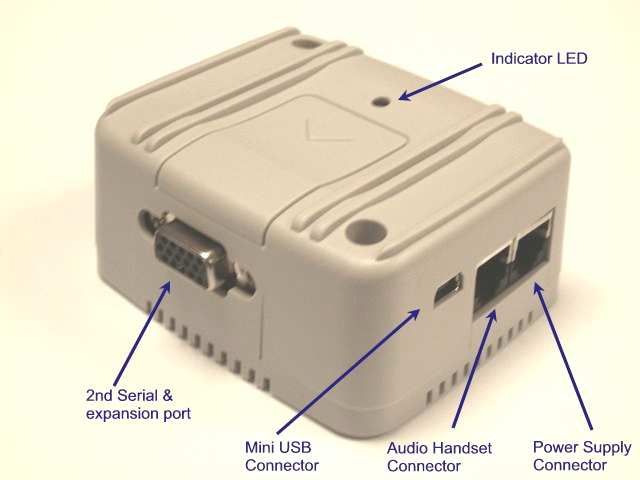
MIX Modem - GSM

   7.2 How to install the modem ................................................................................................ 34
     7.2.1 Power supply ......................................................................................................................................... 34
     7.2.2 Securing the modem .............................................................................................................................. 35
   7.3 Antenna ......................................................................................................................... 35
     7.3.1 General .................................................................................................................................................. 35
     7.3.2 Antenna type .......................................................................................................................................... 35
     7.3.3 Antenna placement ................................................................................................................................ 35
     7.3.4 The antenna cable.................................................................................................................................. 35
     7.3.5 Possible communications disturbances ................................................................................................. 36
8. ACCESSORIES ................................................................................................................................................ 37
   1. POWER SUPPLY ................................................................................................................ 37
     1.1 AC Power Adaptor ................................................................................................................................... 37
     1.2 DC cable ................................................................................................................................................... 37
   2. ANTENNAS ....................................................................................................................... 38
     2.1 Magnetic Dual Band Antenna (900/1800MHz) ........................................................................................ 38
     2.2 Right angle short antenna......................................................................................................................... 38
     2.3 Patch Adhesive Antenna ........................................................................................................................... 38
   3. CABLES ........................................................................................................................... 39
     3.1 SERIAL CABLE ........................................................................................................................................ 39
     3.2 USB CABLE ............................................................................................................................................. 39
     3.3 Expansion port - RS232 2-way Serial Cable ........................................................................................... 39
   4. DEVELOPMENT KITs ......................................................................................................... 40
9, CONFORMITY ASSESSMENT...................................................... ¡ERROR! MARCADOR NO DEFINIDO.
FCC COMPLIANT AND SAR INFORMATION ............................................................................................. 41
10. ROHS STATEMENT ..................................................................................................................................... 42
11. DISPOSAL OF OLD ELECTRICAL & ELECTRONIC EQUIPMENT (WEEE MARK) .................... 42
12. ABBREVIATIONS......................................................................................................................................... 43
13. AT COMMAND SUMMARY ....................................................................................................................... 44
15. SALES CONTACT ......................................................................... ¡ERROR! MARCADOR NO DEFINIDO.

User Manual V.1.1                                                                                                                                 Pag. 3
Subject to change without prior notice
MIX Modem - GSM

1. INTRODUCTION

1.1 Description

The MTX-63I/65I is an intelligent GSM/GPRS control terminal that encapsulates everything you need
for wireless M2M capability in one compact unit.

The MIX MODEM GSM in conjunction with JAVA SDK software package can host and control your
wireless application, minimizing the need for extra components.

Alternatively, it can be used as a powerful standalone GPRS modem with its intrinsic TCP/IP stack.

The MTX-63I/65I is a self contained terminal with its own SIM card reader and 3 standard connectors
interfaces, minimizing the need for further hardware development. This terminal can be used as a
powerful and flexible device that can be used in a wide range of telemetry and telematics applications
that rely on the remote exchange of data, voice, SMS or faxes via the GSM cellular network.

As well as providing a standard RS232 serial communication interface the MTX-63I/65I also has an
audio interface allowing an analogue handset to be connected. Also a USB port is included to allow the
connectivity to all relevant PCs and control boards in office and industrial environments. The MIX
MODEM GSM in their expansion port has a wide and useful range of IOs that can be reconfigured to
add functions and features that make your M2M solution both innovative and cost effective.

The MTX-63I/65I can be used to provide a communications link for a variety of wireless applications
including fleet and asset management, vending, security and alarm monitoring, e-maintenance and
other telemetry applications.

With quad band 900/1800 MHz and 850/1900 MHz, your applications can be used all over the world.

The MIX MODEM GSM incorporates a Cinterion WM MODEM TC module and the MIX MODEM GSM has
a TC65I inside.

Note! Some of the functions described inside this Technical Description are only possible when the
SIM-Card is inserted

1.2. ORDERING INFORMATION

        MTX-65I: 199801116
        MTX-63I: 199801115

Hardware revision: 1.01

Firmware revision:
      MTX-63I: 01.100
      MTX-65I: 01.100

User Manual V.1.1                                                                        Pag. 4
Subject to change without prior notice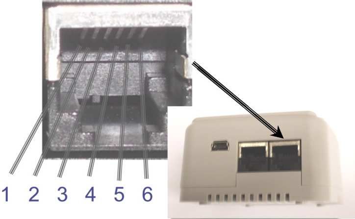
MIX Modem - GSM

1.3 Highlights

Interfaces

• FME M 50 Ohm antenna connector
• Expansion Port: 15-way HD-Dsub: Only for MTX-65I
    4 Digital Input/Output
    2 Analog Input
    1 x I2C/SPI bus
    1 x 2-wires RS232 UART
• RS232 - 9 pin D-sub connector for serial interfaces
(ITU-T V.24 protocol)
• USB mini (2.0 Full-Speed End-Point Compliant)
• Operating status LED
• SIM card interface 3 V, 1.8 V with SIM detection
• Plug-in power supply and on/off interfaces
• Handset audio interface
• VRTC + Alarm

General Features
•   Quad-Band GSM 850/900/1800/1900 MHz
•   GPRS multi-slot class 12
•   GSM release 99
•   Output power:
          - Class 4 (2 W) for EGSM850 & EGSM900
          - Class 1 (1 W) for GSM1800 & GSM1900
•   Control via AT commands (Hayes 3GPP TS 27.007 and 27.005)
•   SIM Application Toolkit (release 99)
•   TCP/IP stack access via AT commands
•   Internet Services: TCP, UDP, HTTP, FTP, SMTP, POP3
•   Supply voltage range: 6 ... 30 V
•   Power consumption (at 12 V):
          - Power down 0,5 mA
          - Sleep mode (registered DRX = 5) 29 mA
          - Speech mode (average) 184 mA
          - GPRS class 12 [Power reduction = 6dB] (average) 330 mA
•   Temperature range
          - Operation: -30°C to +70°C
          - Storage: -40°C to +85°C
•   Dimensions. Excluding connectors:78,1 x 66,8 x 37,2 mm
•   Weight: < 190 g

GPRS data transmission
•   GPRS class 12
•   Mobile station class B
•   PBCCH support
•   Coding schemes CS 1-4

Multiple simultaneous PDP contexts

User Manual V.1.1                                                    Pag. 5
Subject to change without prior notice
MIX Modem - GSM

CSD data transmission
•   Up to 14.4 kbit/s
•   V.110
•   Non-transparent mode
•   USSD support

Specification for fax
•     Group 3, class 1, 2
Voice Features
•   Triple-rate codec for HR, FR, and EFR
•   Adaptive multi-rate AMR
•   Basic hands-free operation
•   Echo cancellation
•   Noise reduction

Short Message Service (SMS) Features
• Point-to-point MO and MT
• SMS cell broadcast
• Text and PDU mode

Internet Protocols
TCP/UDP/IP protocol stack
Extensive AT command access to TCP/IP stack
Internet Services: TCP, UDP, HTTP, FTP, SMTP, POP3

Open application resources (only MTX-65I)
ARM© Core, Blackfin© DSP
• Memory: 400 KB (RAM) and1.7 MB (Flash)
• Improved power-saving modes
Java™ features (only MTX-65I):

• CLDC 1.1 Hl
• J2ME™ profile IMP-NG
• Secure data transmission with HTTPS, SSL and PKI

Over-the-air update (only MTX-65I)

• Application SW: OTAP
• Firmware: FOTA (OMA compliant)

User Manual V.1.1                                             Pag. 6
Subject to change without prior notice
MIX Modem - GSM

   1.4 MTX-63I/65I Wireless modems in a Communication System

   Figure 1 and Figure 2 illustrate the main blocks of a wireless communication system using the wireless
   modem. Figure 1 show the communication system when a micro-controller is used. They also show the
   communication principles of the system and the interface between the wireless modem and the
   application and Figure 2 shows the communication system when the JAVA application is embedded on
   the wireless modem. The definitions in the figures, as used elsewhere in this manual, are in
   accordance with the recommendations of 3GPP TS 27.007.

   The MS (mobile station) represents the wireless modem and SIM card. The wireless modem excluding
   SIM card, is known as the ME (mobile equipment).

   The DTE (data terminal equipment) is the controlling application. This can be either an external host or
   an internal embedded application.

   The DCE (data circuit terminating equipment) is the serial communication interface of the MS.

Figure 1. Main Blocks in a Wireless System (external micro-controller)   Figure 2. Main Blocks in a Wireless System (embedded application)

   1.5 Main Features and Services

   The MTX-63I/65I performs a set of telecom services (TS) according to GSM standard phase 2+, ETSI
   and ITU-T. The services and functions of the MTX-63I/65I are implemented by issuing customized
   applications embedded on the device, or by AT commands issued internally, or over the RS232 serial
   interface.

   1.5.1 Types of Mobile Station

   The MTX-63I/65I is a fully Quad Band capable GSM/GPRS mobile station with the characteristics shown in
   the table below.

   User Manual V.1.1                                                                                           Pag. 7
   Subject to change without prior notice
MIX Modem - GSM

              Feature                      GSM850          E-GSM900       GSM1800         GSM1900

              Frequency         Tx         824-849         880-915        1710-1785       1850-1910
              range (MHz)     Rx 869-894                   925-960        1805-1880       1930-1990
              RF power @ARP with
                                 33dBm                     33dBm          30dBm           30dBm
              50Ω load (typ)
              Channel spacing    200kHz                    200kHz         200kHz          200kHz
              Number of channels           124             174            374             299
              Number of TD slots           8               8              8               8
              Duplex spacing               45MHz           45MHz          95MHz           80MHz
              GSM power class              4 (2W)          4 (2W)         1 (1W)          1 (1W)
              Modulation                   GMSK
              Receive sensitivity
MIX Modem - GSM

1.5.5 GPRS Multi-Slot Support

GSM Multi-slot classes supported by MTX-63I/65I

      Multislot        Maximum slot allocation                Allowable
                                                                                   Max data rate
      Class            Downlink Uplink            Active      Configuration

                                                                                   8-12Kbps Send
      8                4            1             5           1 up; 4 down
                                                                                   32-48Kbps Receive

                                                                                   8-12Kbps Send
                                                              1 up; 4 down
                                                                                   32-48Kbps Receive
      10               4            2             5
                                                                                   16-24Kbps Send
                                                              2 up; 3 down
                                                                                   24-36Kbps Receive
                                                              1 up 4 down
                                                              2 up 3 down          8-12kpbs per slot
      12               4            4             5
                                                              3 up 2 down
                                                              4 up 1 down

1.5.6 Power Consumption

The table below briefly summarizes the various operating modes referred to in the following chapters.

                                               Various power save modes set with AT+CFUN command. Software is active
                                               to minimum extent. If the Terminal was registered to the GSM network in
                                               IDLE mode, it is registered and paging with the BTS in SLEEP mode, too.
                   GSM / GPRS SLEEP            Power saving can be chosen at different levels: The NON-CYCLIC SLEEP
                                               mode (AT+CFUN=0) disables the AT interface. The CYCLIC SLEEP modes
                                               AT+CFUN=7 and 9 alternately activate and deactivate the AT interfaces to
                                               allow permanent access to all AT commands.

                                               Software is active. Once registered to the GSM network paging with BTS is
                   GSM IDLE
                                               carried out. The Terminal is ready to send and receive.
Normal operation
                                               Connection between two subscribers is in progress. Power consumption
                   GSM TALK                    depends on network coverage individual settings, such as DTX off/on,
                                               FR/EFR/HR, hopping sequences, antenna.

                                               Terminal is ready for GPRS data transfer, but no data is currently sent or
                   GPRS IDLE                   received. Power consumption depends on network settings and GPRS
                                               configuration (e.g. multislot settings).

                                               GPRS data transfer in progress. Power consumption depends on network
                                               settings (e.g. power control level), uplink / downlink data rates, GPRS
                   GPRS DATA
                                               configuration (e.g. used multislot settings) and reduction of maximum
                                               output power.

                   Normal shutdown after sending the AT^SMSO command, after pressing the ON/OFF key or after the
POWER DOWN         activation of the ONOFF line. The RTC works continuously, but the software is not active. Interfaces are
                   not accessible.

                   Airplane mode shuts down the radio part, causes the Terminal to log off from the GSM/GPRS network
                   and disables all AT commands whose execution requires a radio connection. Airplane mode can be
                   controlled by the AT commands AT^SCFG and AT+CALA: With AT^SCFG= MEopMode/Airplane/OnStart
Airplane mode      the Terminal can be configured to enter the Airplane mode each time when switched on or reset. The
                   parameter AT^SCFG=MEopMode/Airplane can be used to switch back and forth between Normal mode
                   and Airplane mode any time during operation. Setting an alarm time with AT+CALA followed by
                   AT^SMSO wakes the module up into Airplane mode at the scheduled time.

User Manual V.1.1                                                                                    Pag. 9
Subject to change without prior notice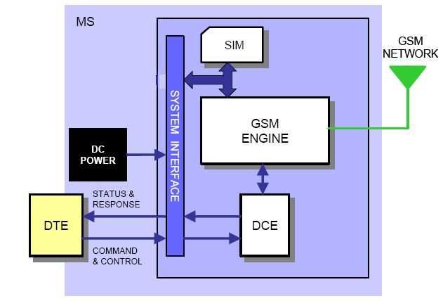
MIX Modem - GSM

Average power consumption

Parameter          Description                 Conditions                         Min   Typ   Max    Unit

                                                                                   6    12    30     V
VPOWER             Operating Voltage           for one minute
                                                                                              36     V

                                                                          @8V

                                               Power Down mode            @12V          TBD          mA

                                                                          @30V

                                                                          @8V

                                               SLEEP mode                 @12V          TBD          mA

                                                                          @30V

                                                                          @8V

                                               IDLE mode                  @12V          TBD          mA

                                                                          @30V

                                                                          @8V
IPOWER
Average supply current (average time 3 min.)   TALK mode                  @12V          TBD          mA
@25°C @ worst case: GSM 900 max power
level                                                                     @30V

                                                                          @8V

                                               Data GPRS 1Tx / 4Rx        @12V          TBD          mA

                                                                          @30V

                                                                          @8V
                                               Data GPRS 2Tx / 3Rx
                                                                          @12V          TBD          mA
                                               (Power reduction = 3dB)
                                                                          @30V

                                                                          @8V
                                               Data GPRS 4Tx / 1Rx
                                                                          @12V          TBD          mA
                                               (Power reduction = 6dB)
                                                                          @30V

                                                                          @8V
                   Peak    supply    current
IPOWER_P           during transmission slot    Power control level for
                                                                          @12V          TBD          mA
(6)                (577µs * No. of Tx every    Pout max
                   4.6ms)
                                                                          @30V

The power consumption figures shown represent typical average current and making different multi-slot
configurations, the worst case being that of two uplink and three downlink slots.

(6) Typical values measured with antenna impedance = 50 Ohm (return loss >20dB)

User Manual V.1.1                                                                                  Pag. 10
Subject to change without prior notice
MIX Modem - GSM
1.4.7 SIM Card
The MTX-63I/65I supports an external SIM card through the integrated SIM holder. Both 3V and 1.8V
SIM technology is supported. Older, 5V SIM technology is not supported
1.5 Precautions
The MTX-63I/65I as a standalone item is designed for indoor use only. To use outdoors it must be
integrated into a weatherproof enclosure. Do not exceed the environmental and electrical limits
specified.
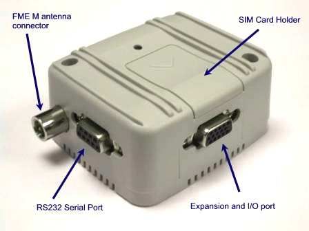
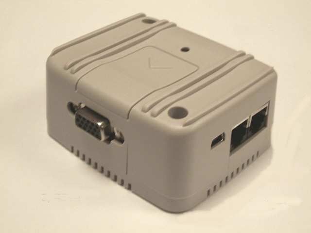
2. MECHANICAL DESCRIPTION
2.1 Overview
The pictures below show the mechanical design of the module along with the positions of the different
connectors and mounting holes. The module case is made of durable PC/ABS plastic.
Figure 3. MTX-63I/65IModule viewed from the right side
Figure 4. MTX-63i/65iModule viewed from the left side
User Manual V.1.1 Pag. 11
Subject to change without prior noticeMIX Modem - GSM
2.2. Dimensions
Figure 5. Dimensions of the MTX-63I/65I terminal in mm
User Manual V.1.1 Pag. 12
Subject to change without prior noticeMIX Modem - GSM 3. ELECTRICAL DESCRIPTION All electrical connections to the module are protected in compliance with the standard air and contact Electrostatic Discharge (ESD). The module uses the following industry standard connectors: • D-Sub 9 pin female (Main RS232 serial port) • High density 15 pin D-Sub(Secondary RS232 UART and extended I/O interface) • RJ12 6-way (power supply connector) • RJ12 4-way (handset connector) • SIM card reader • FME male coaxial jack (antenna connector) 3.1 Power Connector An RJ12 6-way connector, as shown and described below, serves means of supplying and controlling d.c. power to the modem. The supply voltage, VCC, required by the modem is in the range 6-32V d.c. The power supply has to be a single voltage source capable of providing a peak during an active transmission. The uplink burst causes strong ripples (drop) on the power lines. Application of the supply voltage does switch the modem on. Automatic restart after shutdown: This allow to an application to be always switched on resp. to be able to restart by itself. The terminal will not need external ignition to be powered up. The terminal will be powered up 100% time if power is applied. The only way to shut down the terminal is applying continuously positive signal in pin 3 of J1 RJ11 power connector. The powered up with a RTS Pulse has been removed. An active-high control signal, TURN_OFF, can be used to switch modem off when continuously applied, or can be used to perform hardware reset when applied for > 3.5s. User Manual V.1.1 Pag. 13 Subject to change without prior notice
MIX Modem - GSM

PIN:   Signal            Dir      Limits        Description
1      VCC               Input    6-32 V DC     Positive power input
2      Not connected     -
                                                Active high control line used to switch off or
                                                reset the modem
3      TURN_OFF          Input    5 – VCC
                                                VIH > 5V, VIL < 2V
                                                Power off: Continuosly
                                                Internally not connected. Terminal will switch on
4      TURN_ON           Input    5 – VCC
                                                automatically.
                                                Backup the RTC from an external capacitor or a
5      VDDLP             I/O      Vmax 4,3 V
                                                battery (rechargeable or non-chargeable).
6      GND               Input                  Negative power (ground)

Note. VCC and GND are reverse polarity and overvoltage protected.

User Manual V.1.1                                                                        Pag. 14
Subject to change without prior notice
MIX Modem - GSM
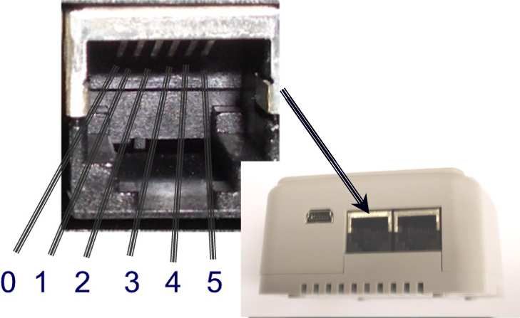
3.2 Audio Connector
A 6-way 4-poles RJ connector, as shown below, allows a telephone handset to be plugged into the
modem, giving access to the microphone and earpiece signals. The connector may also be used to
drive other analogue audio sub-systems or devices.
The audio interface provides one analog input for a microphone and one analog output for an
earpiece.
• The microphone input and the earpiece output are balanced.
• For electret microphones a supply source is implemented.
• The MTX-63I/65I is pre-configured to work with a range of handsets, the audio interface is flexible
and its performance can be configured, using AT commands, to match a particular handset or audio
subsystem.
• Earpiece outputs are short-circuit protected.
Audio handset connection.
Audio signal descriptions are listed below:
Pin Signal Dir Description
0 Not connected
1 MICN I Microphone negative
input
2 EPN O Earpiece negative
output
3 EPP O Earpiece positive
output
4 MICP I Microphone positive
input
5 Not connected
User Manual V.1.1 Pag. 15
Subject to change without prior noticeMIX Modem - GSM
The electrical characteristics of the voiceband part vary with the audio mode. Specifications are listed
in following table. To suit several types of audio equipment, three audio modes given by default can be
selected by the AT command AT^SNFS.
The audio mode 1 are optimized for the reference handset (type Votronic) connected to the MTX-
63I/65I Terminal, and to ensure that the reference parameters are always within the limits demanded
by the standards they cannot be changed by AT command. Furthermore, the reference parameters are
set as factory default.
In audio mode 4 and 5, the gain in the microphone, earpiece and the side tone path can be adjusted
from the cellular device application by using further AT commands.
Please note that the 2nd audio interface of the MODEM TC/65I module is not connected in the MTX-
63I/65I Terminal. Audio modes 2, 3 and 6 can be selected by setting AT^SAIC=2,1,1,
1 (Default settings,
Mode No AT^SNFS= 4 5
not adjustable)
Name Default Handset User Handset Plain Codec 1
Recommended User provided Direct access to
Purpose
handset handset speech coder
Gains programmable via AT command NO YES YES
Sidetone YES YES YES
Volume control NO YES YES
Cancellation and Cancellation and
Echo control (send) NO
suppression suppression
Noise suppression YES YES NO
MIC input signal for 0dBm0 @ 1024 Hz
12.5 mV 12.5 mV 400 mV
(at default gain settings)
Earpiece output signal in mV eff. @
475 mV (default @
0dBm0, 1024 Hz, no load (at default gain 475 mV 1.5 V 6.0 Vpp
max volume)
settings); @ 3.14 dBm0
Sidetone gain (at default settings) 24.9 dB 24.9 dB -∞ dB
User Manual V.1.1 Pag. 16
Subject to change without prior noticeMIX Modem - GSM
The electrical characteristics are given in the table below.
Function Signal IO Parameter Min. Typ. Max. Unit
name
Microphone MICP, I DC (no load) at MICP 5.3 5.4 5.6 V
MICN
DC at MICP in POWER DOWN 0V V
DC (no load) at MICN 0 V
DC Resistance differential MICN, MICP 4.6 4.7 4.8 kOhm
(balanced)
Impedance Zi (balanced) 3.9 4.0 4.1 kOhm
Input level Uimax 0.6 VPP
Restricted Input level Uires 7 1.6 VPP
Gain range 6 dB steps 0 42 dB
Frequency Range 200 3900 Hz
fine scaling by DSP (inCalibrate) -∞ 0 dB
Earpiece EPP, O Impedance (balanced) 8 Ohm
EPN
AC output level UO Gain = 0dB @ 3.14 5.97 VPP
dBm0 no load
Gain range -18 0 dB
Gain accuracy 0.8 dB
Frequency area 200 3900 Hz
DC Offset (balanced) 100 mV
Attenuation distortion for 200...3900Hz 1 dB
Out-of-band discrimination 70 dB
LEAudio Length of Audio (Handset) cable 3 m
Unless otherwise stated, all specified values are valid for gain setting (gs) 0dB and 1kHz test signal.
gs = 0dB means audio mode = 5, inBbcGain= 0, inCalibrate = 32767, outBbcGain = 0, OutCalibrate =
16384, sideTone = 0.
The electrical characteristics of the voiceband part depend on the current audio mode selected by the
AT command AT^SNFS. See Table 9: Audio modes.
The audio modes 4 and 5 can be adjusted by parameters. Each audio mode is assigned a separate
parameter set.
User Manual V.1.1 Pag. 17
Subject to change without prior noticeMIX Modem - GSM
Audio Parameters Adjustable by AT Commands
Parameter Influence to Range Gain Calculation
range
inBbcGain MICP/MICN analog amplifier 0...7 0...42dB 6dB steps
gain of baseband controller
before ADC
inCalibrate digital attenuation of input 0...32767 -∞...0dB 20 * log
signal after ADC (inCalibrate/
32768)
outBbcGain EPP/EPN analog output gain of 0...3 0...-18dB 6dB steps
baseband controller after DAC
outCalibrate[n] Digital attenuation of output 0...32767 -∞...+6dB 20 * log (2 *
n = 0...4 signal after speech decoder, outCalibrate[n]/
before summation of sidetone 32768)
and DAC present for each
volume step[n]
sideTone Digital attenuation of sidetone is 0...32767 -∞...0dB 20 * log
corrected internally by (sideTone/
outBbcGain to obtain a constant 32768)
sidetone independently to
output volume
3.3 Mini USB Connector
TC65 supports a USB 2.0 Full Speed (12Mbit/s) device interface. The USB interface is primarily
intended for use as command and data interface and for downloading firmware. The USB I/O pins are
capable of driving the signal at min 3.0V. They are 5V I/O compliant.
The USB port has different functions depending on whether or not Java is running. Under Java, the
lines may be used for debugging purposes (see [16] for further detail). If Java is not used, the USB
interface is available as a command and data interface and for downloading firmware.
The USB I/O-pins are capable of driving the signal at min 3.0V. They are 5V I/O compliant. To properly
connect the module’s USB interface to the host a USB 2.0 compatible connector is required.
Furthermore, the USB modem driver delivered with MIX MODEM GSM must be installed as described
below.
The USB host is responsible for supplying, across the VUSB_IN line, power to the module’s USB
interface, and all the other MTX-65i interfaces. This is because MTX-65i is designed as a self powered
device compliant with the “Universal Serial Bus Specification Revision 2.0”
User Manual V.1.1 Pag. 18
Subject to change without prior noticeMIX Modem - GSM 3.4 Antenna Connector The antenna connector allows transmission of radio frequency (RF) signals between the modem and an external customer-supplied antenna. The modem is fitted with a 50Ω, FME male coaxial jack. The external antenna must be matched properly to achieve best performance regarding radiated power, DC-power consumption, modulation accuracy and harmonic suppression. 3.5. SIM card reader The MTX-63I/65I Terminal is fitted with a SIM card reader designed for 1.8V and 3V SIM cards. It is the flip-up type which is lockable in the horizontal position and is accessed through a removable panel as shown below. The card holder is a five wire interface according to GSM 11.11. A sixth pin has been added to detect whether or not the SIM card drawer is inserted. Removing and inserting the SIM card during operation requires the software to be reinitialized. Therefore, alter reinserting the SIM card it is necessary to restart MTX65I Terminal. The full operation of the MTX-63I/65I relies on a SIM card being inserted. Some MTX-63I/65I functionality may be lost if you try to operate the control terminal without a SIM card 3.6 MAIN Serial RS232 Interface Port ASC0 The modem supports a standard RS232 serial interface (EIA/TIA 574) via its 9 pin Sub-D connector, shown below. User Manual V.1.1 Pag. 19 Subject to change without prior notice
MIX Modem - GSM

MTX-63I/65I Terminal is designed for use as a DCE. (data circuit-terminating equipment) based on the
conventions for DCE-DTE connections it communicates with the customer application (DTE- data
terminating equipment) using the following signals:
        • Port TxD @ application sends data to TXD of MTX-63I/65I Terminal
        • Port RxD @ application receives data from RXD of MTX-63I/65I Terminal

The RS-232 interface is implemented as a serial asynchronous transmitter and receiver conforming to
ITU-T V.24 Interchange Circuits DCE. It is configured for 8 data bits, no parity and 1 stop bit and can
be operated at fixed bit rates from 300bps to 460,800bps.

Autobauding supports bit rates from 1,2bps to 460,800bps. Hardware handshake using the /RTS and
/CTS signals and XON/XOFF software flow control are supported.

In addition the modem control signals DTR, DSR, DCD and RING are available. The MODEM control
signal RING (Ring Indication) can be used to indicate, to the cellular device application, that a call or
Unsolicited Result Code (URC) is received.

The electrical characteristics of the serial port signals are shown below:
 Note: Outputs at 3kOhm load

                Pin   Signal    Dir      Voltage          Description
                                         levels
                1     DCD       O        Min ±5V          Data carrier detect

                2     RD 0      O        Min ±5V          Received data
                                         VILmax = 0.6V
                3     TD 0      I        VIHmin = 2.4V    Transmitted data
                                         VImax = ±25V
                                         VILmax = 0.6V
                4     DTR       I        VIHmin = 2.4V    Data terminal ready
                                         VImax = ±25V
                5     GND       -        0V               Ground connection

                6     DSR       O        Min ±5V          Data set ready
                                         VILmax = 0.6V
                7     RTS       I        VIHmin = 2.4V    Request to send
                                         VImax = ±25V

                8     CTS       O        Min ±5V          Clear to send

                9     RI        O        Min ±5V          Ring indicator

User Manual V.1.1                                                                         Pag. 20
Subject to change without prior notice
MIX Modem - GSM
Features
• Includes the data lines TXD0 and RXD0, the status lines RTS0 and CTS0 and, in addition, the modem
control lines DTR0, DSR0, DCD0 and RING0.
• ASC0 is primarily designed for controlling voice calls, transferring CSD, fax and GPRS data and for
controlling the GSM engine with AT commands.
• Full Multiplex capability allows the interface to be partitioned into three virtual channels, yet with
CSD and fax services only available on the first logical channel. Please note that when the ASC0
interface runs in Multiplex mode, ASC1 cannot be used.
• The DTR0 signal will only be polled once per second from the internal firmware of MTX-63I/65I.
• The RING0 signal serves to indicate incoming calls and other types of URCs (Unsolicited Result
Code). It can also be used to send pulses to the host application, for example to wake up the
application from power saving state. To configure the RING0 line use following AT Command:
AT^SCFG.
• By default, configured for 8 data bits, no parity and 1 stop bit. The setting can be changed using the
AT command AT+ICF and, if required, AT^STPB. .
• ASC0 can be operated at fixed bit rates from 300 bps to 460800 bps.
• By default, serial speed for MTX-63i is autobauding: supports bit rates from 1200 to 460800 bps.
For MTX-65i is 115200bps
• Autobauding is not compatible with multiplex mode.
• Supports RTS0/CTS0 hardware flow control and XON/XOFF software flow control.
3.7 Expansion I/O port
MTX-63I/65I includes second 2-wire RS232 interface. on the 15 pin high density connector together
with I2C bus and VTRC. The MTX-65I supports a range of configurable I/Os plus SPI bus.
1. I2CCLK SPICLK 6. I2CDAT-SPIDO 11. IO 2
2. RD1 7. SPIDI 12. IO 4
3. TD1 8. SPICS 13. ADC 2
4. IO 1 9. VEXT 14. GND
5. IO 3 10. DAC_OUT 15. ADC 1
User Manual V.1.1 Pag. 21
Subject to change without prior noticeMIX Modem - GSM
MTX-63V3 MTX-65I
Pin Dir Max. Voltage limits Description
Signal Signal
I2CCLK I2CCLK I2C or SPI bus clock signal
1 O 0.2 - 3.05 V
SPICLK
Secondary RS232 ASC1 UART signal:
2 RD1 RD1 O Min ±5V
Received data
VILmax = 0.6V Secondary RS232 ASC1 UART signal
3 TD1 TD1 I VIHmin = 2.4V Transmitted data.
VImax = ±25 V IL < 0.6V, V IH > 2.4V
Input: 0.8 - 3.05
4 GPIO 1 I/O Digital input/output I/O 1
Output: 0.2 - 3.05
Input: 0.8 - 3.05
5 GPIO 3 I/O Digital input/output I/O 3
Output: 0.2 - 3.05
Input: 0.8 - 3.05V
6 I2CDAT I2CDAT-SPIDO I/O I2C data or SPI bus Data Output
Output: 0.2 - 3.05V
7 SPIDI I 0.8 - 3.05V SPI bus Data Input
SPI bus Chip Select (master)
8 SPICS O 0.3 – 3.05V
2.75 – 3.05V
9 VEXT VEXT O Output Voltage reference
Io max: -50mA
Digital Analog Converter /
10 DAC_OUT O 0.2 – 3.05V
PWM signal output
Input: 0.8 - 3.05
11 GPIO 2 I/O Digital input/output I/O 2
Output: 0.2 - 3.05
Input: 0.8 - 3.05
12 GPIO 4 I/O Digital input/output I/O 4
Output: 0.2 - 3.05
Vimin = 0V, VImax = 2.4V
Ri ≈ 750kOhms
Measurement interval:
100ms – 30s
13 ADC 2 I Analog-Digital converter Input 2
Sensitivity, accuracy: 2400
steps (1step = 1mv)
Accuracy: ± 0.5mV
14 GND GND 0V Ground connection
Vimin = 0V, VImax = 2.4V
Ri ≈ 750kOhms
Measurement interval:
100ms – 30s
15 ADC 1 I Analog-Digital converter Input 1
Sensitivity, accuracy: 2400
steps (1step = 1mv)
Accuracy: ± 0.5mV
User Manual V.1.1 Pag. 22
Subject to change without prior noticeMIX Modem - GSM
3.7.1. SECONDARY SERIAL RS232 INTERFACE ASC1
The ASC1 interface is available as a 2-wire unbalanced, asynchronous modem interface
ASC1 conforming to ITU-T V.24 protocol DCE signalling.
Pin Name Direction Function
Secondary RS232 UART signal:
2 RD1 I ±5 v
Received data
Secondary RS232 UART signal
3 TD1 o ± 25V Transmitted data.
V IL < 0.6V, V IH > 2.4V
Features
• Includes only the data lines TD1 and RD1 Supports only XON/XOFF software flow control.
• On ASC1 no RING line is available. The indication of URCs on the second interface
depends on the settings made with the AT^SCFG command.
• Configured for 8 data bits, no parity and 1 or 2 stop bits.
• ASC1 can be operated at fixed bit rates from 300 bps to 460800 bps. Autobauding is not
supported on ASC1.
3.7.2. I2C Serial Control Bus
I2C is a serial, 8-bit oriented data transfer bus for bit rates up to 400kbps in Fast mode. It
consists of two lines, the serial data line I2CDAT and the serial clock line I2CCLK.
The MTX-63I/65I module acts as a single master device, e.g. the clock I2CCLK is driven by module.
I2CDAT is a bi-directional line.
Each device connected to the bus is software addressable by a unique 7-bit address, and simple
master/slave relationships exist at all times. The module operates as master-transmitter or as master-
receiver. The customer application transmits or receives data only on request of the module.
MTX-
Pin 63I/65I Dir Max. Voltage limits Description
Signal
I2C bus clock signal
1 I2CCLK O 0.2 - 3.05 V
Input: 0.8 - 3.05V
6 I2CDAT I/O I2C data bus
Output: 0.2 - 3.05V
14 GND 0V Ground connection
To configure and activate the I2C bus use the AT^SSPI command. If the I2C bus is active the two
lines I2CCLK and I2DAT are locked for use as SPI lines. Vice versa, the activation of the SPI locks both
lines for I2C.
The I2C interface is powered from an internal VEXT supply line so the I2C interface will be properly
shut down when the module enters the Power-down mode.
User Manual V.1.1 Pag. 23
Subject to change without prior noticeMIX Modem - GSM
Signal
Function IO Signal form and level Comment
name
I2CDAT is configured as pen Drain
RO ≈ 33Ω and needs a pull-up resistor in the
VOLmax = 0.25V at I = 2mA host application.
I2CCLK O
VOHmin = 2.50V at I = -0.5mA According to the I2C Bus
VOHmax = 3.05V Specification Version 2.1 for the fast
mode a rise time of max. 300ns is
I2C permitted. There is also a maximum
interface VOL=0.4V at 3mA specified.
RO ≈ 33Ω VOLmax = 0.25V at The value of the pull-up depends on
I = 2mA VILmax = 0.8V the capacitive load of the whole
I2CDAT I/O system (I2C Slave + lines). The
VIHmin = 2.0V VIHmax =
3.05V maximum sink current of I2CDAT
and I2CCLK is 4mA.
If lines are unused keep pins open.
3.7.3. SPI Bus ONLY MTX-65I
The SPI (serial peripheral interface) is a synchronous serial interface for control and data transfer
between the MTX-65I Terminal and the connected application. Only one application can be connected
to the module’s SPI. The interface supports transmission rates up to 6.5Mbit/s.
It consists of four lines, the two data lines SPIDI/SPIDO, the clock line SPICLK and the chip select line
SPICS.
The MTX-65I Terminal acts as a single master device, e.g. the clock SPICLK is driven by module.
Whenever the SPICS pin is in a low state, the SPI bus is activated and data can be transferred from
the module and vice versa. The SPI interface uses two independent lines for data input (SPIDI) and
data output (SPIDO).
To configure and activate the SPI bus use the AT^SSPI command. If the SPI bus is active the two
lines I2CCLK and I2DAT are locked for use as I2C lines.
In general, SPI supports four operation modes. The modes are different in clock phase and clock
polarity. The module’s SPI mode can be configured by using the AT command AT^SSPI. Make sure the
module and the connected slave device works with the same SPI mode.
User Manual V.1.1 Pag. 24
Subject to change without prior noticeMIX Modem - GSM
Following picture shows the characteristics of the four SPI modes. The SPI modes 0 and 3 are the
most common used modes.
<
The SPI interface is only available if the pins 7 and 8 of the IO interface connector are not
used as I2C interface.
Signal name Pin Description
SPICS 8 Chip select – selects and activates the external device via a low signal.
SPIDI 7 Data in – serial data input line (from the external device to the MIX
MODEM GSM Terminal)
I2CDAT_SPIDO 6 Data out – serial data output line (from the MIX MODEM GSM Terminal
to the external device)
I2CCLK_SPICLK 1 Serial clock line
3.7.4. General Purpose IO (ONLY MTX-65i)
MIX
Max. Voltage
Pin MODEM Dir Description
limits
GSM Signal
Digital Input/Output I/O 1
4 IO 1 I/O -0.5 - VREF
Digital VREF
Digital Input/Output I/O 2
11 IO 2 I/O -0.5 - VREF
Digital VREF
Digital Input/Output I/O 3
5 IO 3 I/O -0.5 - VREF
Digital VREF
Digital Input/Output I/O 4
12 IO 4 I/O -0.5 - VREF
Digital VREF
10 DAC OUT O Digital to Analog Output Converter
The MTX-65I Terminal provides 4 GPIO pins at the IO interface connector. Each GPIO line is ESD
protected and a serial resistor of 100 Ohm is added. This avoids short circuits and is especially
important in the first stages of development where the Java application is not yet fully implemented.
The signal direction (input/output) of the GPIO lines is selectable with AT commands
User Manual V.1.1 Pag. 25
Subject to change without prior noticeMIX Modem - GSM The GIPO related AT commands are the following: AT^SPIO, AT^SCPIN, AT^SCPOL, AT^SCPORT, AT^SDPORT, AT^SGIO, AT^SSIO. When the MTX-65I starts up, all GPIO pins are set to high-impedance state after initializing, so, they’re connected internally with a pull-down resistor. This is necessary to keep these pins from floating or driving any external devices before all settings are done by AT command (at least AT^SPIO, AT^SCPIN), and after closing the GPIOs again. All general purpose IO (GPIO) is programmable by the user. GPIO is programmable for the following features: • An input or output • Level-sensitive or transition-sensitive • Open drain or direct drive • Polarity (inversion) • Internal pull-up resistors 3.7.5. Analog-to-Digital Converter (ADC) The ADC of the MIX MODEM GSM consists of 2 independent, unbalanced, multiplexed analog inputs that can be used for measuring external DC voltages in the range of 0mV…+2400mV. The ADC has a resolution of 12 bits. Use the command AT^SRADC described in [1] to select the analog inputs ADC1_IN or ADC2_IN, to set the measurement mode and read out the measurement results. The measured values are indicated in mV. There is no out of range detection. Voltages beyond these limits cannot be measured: • Underflow: Values ≤ -25mV • Overflow: Values > 2425mV The sample period is adjustable from 30s up to 100ms by AT^SRADC Only during sample time (ts~400µs) the S&H Switch is closed. User Manual V.1.1 Pag. 26 Subject to change without prior notice
MIX Modem - GSM

3.7.6 Real Time Clock

The MTX-63I/65I contains a real time clock (RTC) to maintain accurate timekeeping and to enable
“time stamping” of messages.

The RTC is powered with the signal VRTC present in pin 5 of the POWER CONNECTOR.
The user must connect this pin to an external energy device like a battery or super-capacitor to
provide back-up power to maintain the RTC. Example: If using a 300mF super cap the RTC can be
maintain for at least 12 hours.

The internal Real Time Clock of MTX-63I/65I is supplied from a separate voltage regulator in the
analog controller which is also active when MTX-63I/65I is in POWER DOWN status. An alarm function
is provided that allows to wake up MTX-63I/65I to Airplane mode without logging on to the GSM
network.

In addition, you can use the VDDLP pin on the Power Connector to backup the RTC from an external
capacitor or a battery (rechargeable or non-chargeable). The capacitor is charged by the BATT+ line of
MODEM TC/65I. If the voltage supply at BATT+ is disconnected the RTC can be powered by the
capacitor.

The size of the capacitor determines the duration of buffering when no voltage is applied to MTX-
63I/65I, i.e. the larger the capacitor the longer MTX-63I/65I will save the date and time.
A serial 1kΩ resistor placed on the board next to VDDLP limits the charge current of an empty
capacitor or battery.

The following figures show various sample configurations.

The MTX-63I/65Ican accommodate this battery or super-cap inside, and the MTX-63I/65Ican be
ordered with this special option by request. Please contact your sales nearest distributor.

User Manual V.1.1                                                                      Pag. 27
Subject to change without prior notice
MIX Modem - GSM

3.8. Software Updates

It is possible and sometimes necessary to update the MTX-63I/65I software.
Updates must be carried out by an approved technician.
Please contact your supplier for details Service/Programming

User Manual V.1.1                                                            Pag. 28
Subject to change without prior notice
MIX Modem - GSM

4. OPERATION

4.1 Switching On the Modem

MTX-63V3 & MTX-65I terminal switch on once power is applied (pin 1 & pin 6 J1 power connector)

The modem is fully operational after 4 seconds. Logging onto a network may take longer than this and
is outside the control of the modem.

Automatic restart after shutdown:
• This allow to an application to be always switched on resp. to be able to restart by itself.
The terminal will not need external ignition to be powered up.
The terminal will be powered up 100% time if power is applied. The only way to shut down the
terminal is applying continuously positive signal in pin 3 of J1 RJ11 power connector.
The powered up with a RTS Pulse has been removed.

4.2 Switching Off the Modem

There is 1 way to switch off (power down) the modem as described below:

• Or assert TURN_OFF, pin 3 of power supply connector, continuously high. A delay of up to 10s is
experienced as the modem logs off the network.

We recommend not to use this unless emergency cases.

4.3 Operating States/LED

The modem has a green LED, which displays the operating status of the Terminal.
The LED can be operated in two different display modes: AT^SSYNC=1 or AT^SSYNC=2 (factory
default).

 mode                                              LED Status
                    SYNC mode:
                    Enables the SYNC pin to indicate growing power consumption during a transmit
                    burst. You can make use of the signal generated by the SYNC pin, if power
                    consumption is your concern. To do so, ensure that your application is capable of
 AT^SSYNC=0
                    processing the signal. Your platform design must be such that the incoming signal
                    causes other components to draw less current. In short, this allows your application
                    to accommodate current drain and thus, supply sufficient current to the GSM engine
                    if required.
                    Note: =0 is the factory default of the TC65 module.
                   LED mode:
                   Enables the SYNC pin to drive a status LED installed in your application according to
 AT^SSYNC=1
                   the specifications provided in [2].
                   The coding of the LED is described in Section 19.6.1, ME status indicated by
                   status LED patterns.
                   LED mode:
                   Like =1, but, additionally, enables different LED signalization in SLEEP
 AT^SSYNC=2
                   mode depending on the status of PIN authentication and network registration.
                   Please see AT+CFUN for details on SLEEP mode.
                   Note: =2 is the factory default of the MIX MODEM GSM Terminal.

User Manual V.1.1                                                                       Pag. 29
Subject to change without prior notice
MIX Modem - GSM
In following table is showed the different operating status and changing this mode
ME operating status if ME operating status if
LED behavior
AT^SSYNC=1 AT^SSYNC=2
ME is in one of the following modes: -
POWER DOWN mode
ME is in one of the following modes: -POWER
AIRPLANE mode
DOWN mode
Permanently off CHARGE ONLY mode
AIRPLANE mode
NON-CYCLIC SLEEP mode
CHARGE ONLY mode
CYCLIC SLEEP mode with no temporary
wake-up event in progress (1)
Limited Network Service: No SIM card
inserted or no PIN entered, or network
600 ms on / 600ms off Same as for AT^SSYNC=1
search in progress, or ongoing user
authentication, or network login in progress
IDLE mode: The mobile is registered to the
75 ms on / 3 s off GSM network (monitoring control channels Same as for AT^SSYNC=1
and user interactions). No call is in progress.
75 ms on / 75 ms off / 75
One or more GPRS PDP contexts activated. Same as for AT^SSYNC=1
ms on / 3 s off
500 ms on / 50 ms off Packet switched data transfer is in progress Same as for AT^SSYNC=1
Depending on type of call: Voice call:
Connected to remote party. Data call:
Permanently on Connected to remote party or exchange of Same as for AT^SSYNC=1
parameters while setting up or
disconnecting a call.
SLEEP mode is activated (AT+CFUN
parameter ≠ 1), but the ME is not
ms on / ms off Not possible: With AT^SSYNC=1, LED registered to the GSM network (e.g. SIM not
(2) signalization is disabled in SLEEP mode. inserted or PIN not entered, and therefore,
either no network service or only Limited
Network Service is avail-able.
1) When a temporary wake-up event (for example a call, a URC, a packet switched transfer) occurs in CYCLIC SLEEP mode
the LED flashes according to the patterns listed above. See Section 2.9.1, Wake up the ME from SLEEP mode for details
on the various SLEEP modes and wake-up events.
2) The duration of and depends on the network: In SLEEP mode, the module can only change its LED status during
intermittent wake-up periods when listening to paging information from the base station. Therefore the values of and
vary as follows:
= value from 471 ms to 2118 ms
= 3000 ms
User Manual V.1.1 Pag. 30
Subject to change without prior noticeMIX Modem - GSM
5. EMBEDDED APPLICATIONS. ONLY MTX-65I
The MTX-65I can embed an internal application written in popular JAVA language. Java technology and
several peripheral interfaces on the module allow you to easily integrate your application.
This way, the customer application can be reduced because all the resources: Microcontroller, Flash &
RAM memory and all kind of I/O and bus peripheral is allowed to use by the customer.
This solution saves the external intelligence with all the associate costs and also saving space and
power consumption.
Open application resources
• ARM© Core, Blackfin© DSP
• Memory: 400 KB (RAM) and 1.7 MB (Flash)
• Improved power-saving modes
Java™ features:
• CLDC 1.1 Hl
• J2ME™ profile IMP-NG
• Secure data transmission with HTTPS, SSL and PKI
Over-the-air update
1. Application SW: OTAP
2. Firmware: FOTA (OMA compliant)
User Manual V.1.1 Pag. 31
Subject to change without prior noticeMIX Modem - GSM 6 SAFETY AND PRODUCT CARE Please read the information in this section and the information in “Installation of the Modem”, before starting your integration work! 6.1. Safety instructions PLEASE READ THESE SAFETY INSTRUCTIONS AND KEEP A COPY OF THEM. • Always ensure that use of the modem is permitted. The modem may present a hazard if used in proximity to personal medical electronic devices. As a rule, the modem must not be used in hospitals, airports or planes. • Never use the modem at a gas station, refuelling point, blasting area or in any other environment where explosives may be present. • Operating the modem close to other electronic devices, such as antennas, television sets, and radios may cause electromagnetic interference. • This product is intended to be used with the antenna or other radiating element at least 20cm away from any part of the human body. In applications where this rule cannot be applied, the application designer is responsible for providing the SAR measurement test report and declaration. • You are responsible for observing your country's safety standards, and where applicable, the relevant wiring rules. 6.2. General precautions The MTX-63I/65I Terminal as a stand alone item is designed for indoor use only. To use outside it must be integrated into a weatherproof enclosure. Do not exceed the environmental and electrical limits as specified in “Technical Data”. • Avoid exposing the modem to lighted cigarettes, naked flames or to extreme hot or cold temperature. • Never try to dismantle the modem yourself. There are no components inside the modem that can be serviced by the user. If you attempt to dismantle the modem, you may invalidate the warranty. • The MTX-63I/65I Terminal must not be installed or located where the surface temperature of the plastic case may exceed 85°C. • All cables connected to the MTX-63I/65I Terminal must be secured or clamped, immediately adjacent to the modem's connectors, to provide strain relief and to avoid transmitting excessive vibration to the modem in the installation • Ensure the d.c. cable, supplying power to the MTX-63I/65I Terminal, does not exceed 3 meters. • To protect power supply cables and meet the fire safety requirements when the unit is powered from a battery or a high current supply, connect a fast 1.25A fuse in line with the positive supply. • Do not connect any incompatible component or product to the MTX-63I/65I Terminal. Note! MTX-63I/65Idistributors and sales offices may refuse warranty claims where evidence of product misuse is found. 6.3. SIM card precautions Before handling the SIM card in your application, ensure that you are not charged with static electricity. Use proper precautions to avoid electrostatic discharges. • When the SIM card hatch is opened, the SIM card connectors lie exposed under the SIM card holder. User Manual V.1.1 Pag. 32 Subject to change without prior notice
You can also read