DESIGN CHANGES FOR LARASIC - VENKATA NARASIMHA MANYAM EMAIL: INDICO-FNAL
←
→
Page content transcription
If your browser does not render page correctly, please read the page content below
Design changes for LArASIC
       Venkata Narasimha Manyam
                                    On Behalf of BNL Cold Electronics Team

           Email: vmanyam@bnl.gov

                                                       Feb 8th, 2021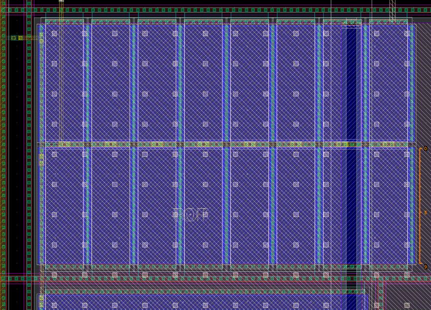
Outline
• LArASIC P4 – Design targets, Identified issues and Improvements

• Main changes leading to LArASIC P5
   • Removing of RQI subtraction

   • SEDC noise and stability

   • Test Charge Injection Pulser DAC

• Status

• Summary

                                                                    2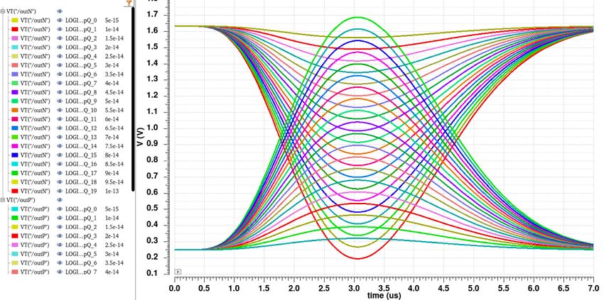
LArASIC P4 – Design targets, Identified Issues and Improvements
• Design targets for P4
   • Address BGR failures happening in ~7% of the chips

   • Address ledge effect (saturation) during shower event observed in ProtoDUNE operation

   • Add single-ended to differential converter (SEDC) to differentially drive ADC (COLDADC)

   • Improve baseline dispersion and shift for different settings
• Observed issues in P4(*)
   • Some channels non-operational in LN2         Sufficiently measured
                                                   & got well understood
   • SEDC significantly noisier than expected

• Planned after P4
   • Modify Test Charge Injection Pulser DAC (nonlinearity for smallest charges)
                                                                                   *Refer H. Chen, 11-30-2020

                                                                                                                3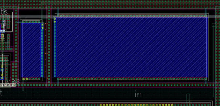
Brief note on SPICE-type simulation models
• Early LARASIC developed with rf018.scs BSIM3 (V3.24) model deck
   • Not able to reproduce ledge effect – models not used any more
• Currently cmn018_assp_v1d2.scs BSIM4 (V4.5) model deck is used
   • Ledge effect could be reproduced
   • BJT models were modified to avoid simulation nonconvergence when temperature is lowered
     and not completely accurate in cold
• Latest cmn018_assp_v1d3.scs model from TSMC is BSIM4 (V4.5)
   • No difference v1d2 vs. v1d3 observed
   • Needed BJT modification
   • Used for DAC Pulser
• New compact PSP RT/LN2 model deck from LOGIX/FNAL/LBNL recently
   • Extracted for two temperatures 25C and -189C
   • Only MOS but process corner and mismatch statistics not included
   • Non MOS components (Res, BJT, MIM cap.) TSMC v1d2 used

                                                                                           4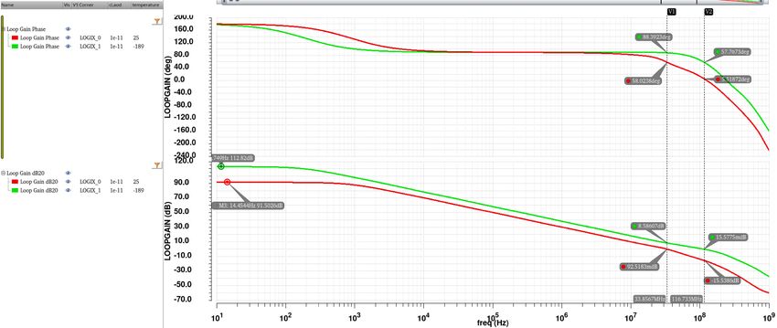
Disconnection of RQI subtraction

                                   5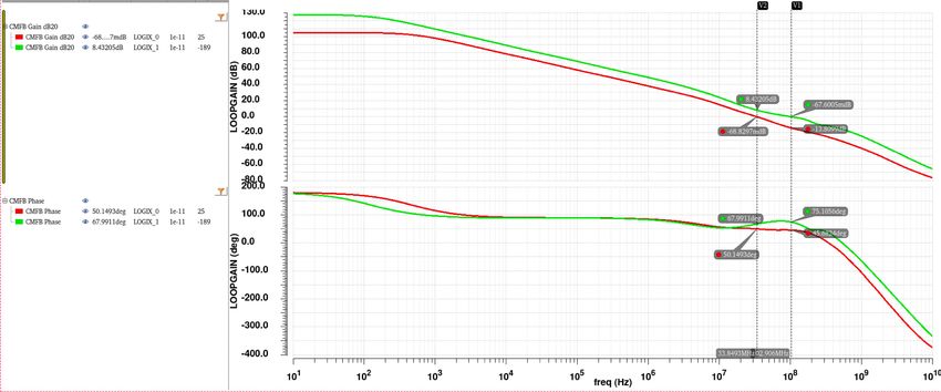
P4 LArASIC in LN2

• Few channels in P4 LArASIC stop working as T decreases (below T=-70C and down to LN2T)
• Measurements revealed variations of RQI values in LN2 even 10x higher than RT
   • RQI x 16 (subtraction circuit) < 20 x RQI (feedback circuit) → violation may happen
• 1 GOhm resistor at input brings all channels working properly in LN2
• In P5 16x RQI subtraction is disconnected (no other modifications attempted)
   • After disconnecting of 16x RQI subtraction, the baseline dispersion will be similar to P2/P3 LArASIC 6
RQI Prebias current for stage 1 CSA
Why this inequality IRQI x 16 (subtraction circuit) < 20 x IRQI (feedback circuit) is violated at LN2T?
• Not accessible for full characterization
• Prebias IRQI transistors are very long L=9um and are operated in very weak inversion at currents 100 pA – 5 nA
• Input side made of one isolated MRQI without dummies, whereas output side made of 2x8 MRQI in closest proximity
  and with one large plate of polysilicon gate and metal 5&6 layers (MIM cap) over all transistors => mechanical stress
  @LN2T may lead to differences in currents

                                                                                      Layout similar to P1

                Input side of ca1                                                       Output side of ca1         7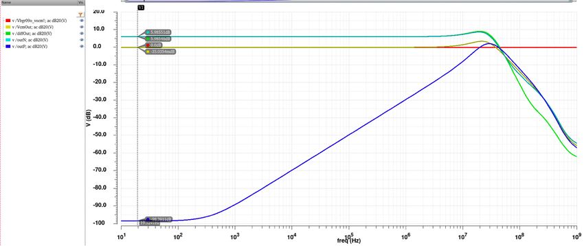
Single-Ended to Differential
Converter (SEDC) Buffer Design

                                 8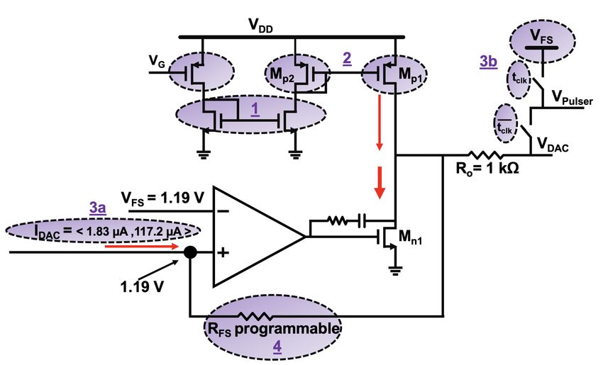
SEDC Buffer – Reasons, Shaper drivability and load from COLDADC
• Convert single-ended (SE) output of the shaper to differential output to drive
  COLDADC SHA (Sample and Hold Amplifier)
• Reasons:
   • To suppress common mode pickup that may be affecting single ended signals between
     LArASIC-ADC.
• Shaper output
   • DC coupled (preferred configuration)
   • Output impedance of 1kΩ (in fact it is RC LPF of 1kΩ and 50 pF)
       • Challenging to design SEDC based on resistive feedback
• COLDADC SHA
   • SHA is a switched-capacitor circuit, the load to the SEDC will look resistive.
   • The effective resistance will be 1/fC where C is the load (2 pF) and f is the sampling rate (2
     MHz), so the zeroth order model would be a 250 kΩ resistor to ground – C. Grace, LBNL
   • Pessimistically, accounting for trace impedance owing to chip-to-chip drivability, 10-20 pF
     load is assumed along with 250 kΩ resistor to ground on each output of SEDC

                                                                                                      9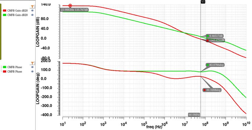
Single-Ended to Differential Converter (SEDC) Buffer in P4
• OpAmp: Based on single-ended buffer core already present in LARASIC,
• Highly linear and silicon-proven rail-to-rail operation → Risk mitigation to deal with the known
• Modified for differential output and addition of Common-Mode Feedback Circuit (CMFB)
• Architecture: Psuedo-differential (Asymmetric) buffer based on COLDADC iBuff SDC
Bias
SEDC OpAmp
CMFB
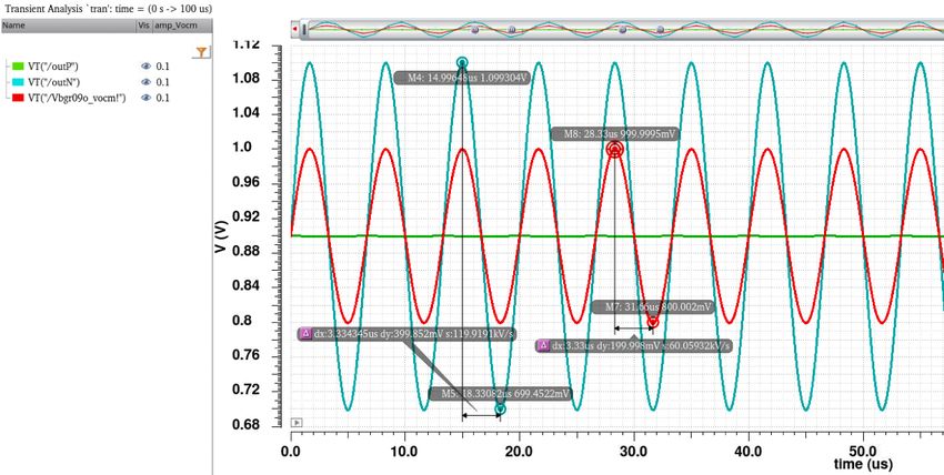
10P4 LArASIC – SEDC with workaround
Die #4, Ch 04, at RT on board #2
RQI = 500 pA, BL = 900 mV, Gain = 14 mv/fC
Internal pulser, tPeak = 1 µs
Vp-p = 2 x 1.246 V
2 OutP from analog monitor
150mV/div
4 SEDC output with (Differential probe)
300mV/div
1. Bypass caps of 100nF and 1uF on top and bottom
VDDO pins on daughter board/analog mezzanine
with wire-bonded die
2. 470 pF load on all OutPs to GND and OutNs to
GND, NO cap in b/w OutPs and OutNs
3. VDDO reduced to 1.6 V, power consumption ~11
mW/ch consistent with simulation
Observed high frequency noise
without workaround
11Understanding Pseudo-differential (Asymmetric) buffer Architecture
B
A
C
• Pros:
• Does not require resistors setting feedback paths,
• Does not require a preceding stage able to drive resistive loads
• Pure capacitive input
• Cons:
• There is CM (common-mode) to DM (differential-mode) gain
• VOCM does not shift both outputs and any change of VOCM goes 2x to vOutN
as B follows C and vOutP does so, but vOutN =(VOCM +(VOCM -VIN)/2)
• VOCM must be extremely clean not to contribute to noise as any variation on VOCM is not eliminated
differentially by subtracting vOutP - vOutN as in typical fully-differential amplifiers
• Both paths differential and common mode must have equally high open loop gains for
precision and linearity
• No elimination of even-order harmonic distortion
12CM to DM gain problem – Example simulation
A spurious tone injected on
VOCM, Fspur, VOCM = 150 kHz
*At RT with TSMC BSIM4 models
Vocm AC spurious signal is not visible at outP and is not rejected at outN but doubled → it is required adding a large RC filter on Vocm on each channel
13CM to DM gain problem – AC analysis VOCM not reflected on outP, hence reflected on differential output 14
Proposed VOCM filtering scheme for P5:
                                                                          R         VOCM_15   - +   vOutP
                                                                                                    vOutP15
                                                                                    SH15      + -   vOutN
                                                                                                    vOutN15
                                                                              C

                                                                        Channel
• Existing filtering (output of bias generator):                            RC
                                                                        Filtering
   • R0|C0 yields f3dB = 1.25kHz,                                        Added
• Now added:                                                              R         VOCM_1    - +   vOutP
                                                                                                    vOutP1

   • R|C in every channel with R=2MW and C≅65pF                                      SH
                                                                                     SH1      + -   vOutN
                                                                                                    vOutN1
     (max that can fit empty space in layout)                                 C

   • Provides sufficient suppression of VOCM
                                                                          R         VOCM_0    - +   vOutP
                                                                                                    vOutP0
                                                                                     SH
                                                                                     SH0      + -   vOutN
                                                                                                    vOutN0
                                                                              C

                                                - +           R0
                                                                        VOCM
                                       VBGR09
                                                      VBGR09_BUF
                                                + -
                                                                   C0
                                                                                                              15
With RC filtering – P5 SEDC
Sufficient local
suppression obtained
100x100 µm2 rphpoly +
moscap RC LPF w. added at
the VOCM
This plot is for f3dB=5kHz (now f3dB=1.25kHz further suppression obtained)
16P4 SEDC CMFB Loop Stability problem
• As both paths differential and
common mode must have ND pole from CMFB output
equally high open loop gains
for precision and linearity, Analysis of CMFB
loop with used
in quest for increasing CM CMFB scheme
path gain stability got reduced compared with
ideal CMFB
• CMFB needs attention
• CMFB error amplifier output
non-dominant pole fell low in
freq. and needs to be
corrected – fully understood W/ used CMFB
now
W/ Ideal CMFB
17P5 SEDC changes
CMFB
P4 CMFB -> P5 CMFB classical solution used: M. Banu, J. M. Khoury, and Y. Tsividis, “Fully differential operational amplifiers with
Changes from P4 to P5: accurate output balancing,” IEEE J. Solid-State Circuits, vol. 23, no. 6, pp. 1410–1414, Dec. 1988, doi: 10.1109/4.90039.
1. Rcomp increased by 4x
2. CMFB tail m factor increased from 32 to 48
3. CMFB tail casc. removed Improves stability
4. CMFB Load changed to diode connected &
5. CMFB amplifier gain boosted with R addition to source and current subtraction CM noise rejection
6. Filter on CMFB reference (Vocm) added and improved to have f3dB ≅ 1.25 kHz
18P5 SEDC Main loop Stability:
Good PM for stability
For 10 pF || 250 kΩ load
RT
LAr
*PSP Logix models for MOS and the rest TSMC models 19P5 SEDC CMFB loop stability
Good PM for stability
For 10 pF || 250 kΩ load
RT
LAr
*PSP Logix models for MOS and the rest TSMC models 20SEDC P5 Schematic and Post-layout (PEX) STB 10pF||250kOhm
Schematic
PEX (RCc*)
Simulations indicate good stability at schematic and extraction
level with LOGIX and TSMC models at RT and LAr
*RCc = All Parasitics {Res + Cap + Cap coupled to ground}
21Linearity with FE channel at -189 ℃: SEDC output for 20pF||250kΩ load for Tp=2µs
Setting: BL = 200 mV, Gain = 14 mV/fC, RQI = 500pA, Cdet = 150 pF
SEDC extracted RCc
and rest in sch
Simulations show linear operation
Logix models for LAr 22
22Linearity with FE channel at -189 ℃: SEDC output for 20pF||250kΩ load for Tp=2µs
Setting: BL = 200 mV, Gain = 14 mV/fC, RQI = 500pA, Cdet = 150 pF
Differential output Logix models for LAr
SEDC extracted RCc
and rest in sch
INL LAr ≅ ± 0.04 %,
Compatible with COLDADC
23
23Pulser DAC improvement
24Identified Issues with Pulser implemented in P1
1. NMOS VG improperly biased as it is connected to a PMOS gate
2. Minimum channel length used in Mp1 and Mp2 and hence poor current source
3. Mn1 goes into cutoff deep triode region when IDAC is about max (117.2 µA)
• Nonlinearity of first three levels → observed in measurements
Nonlinearity of first three levels
25Improved Pulser for LArASIC P5
1. Properly biased with current source
2. Increased channel length to 2 µm for
in Mp1 and Mp2
3. To improve linearity of first three steps
a. Switching currents in opposite
direction (min. to max.)
b. Switch clock inverted, along with
connecting VPulser to VFS instead of Vss
during tclk
4. RFS programmability to match channel
swings added with appropriate t-gate
switches
26Pulser DAC programmability and simulations
DAC gain matched with gain setting of Ch0 (SG0, SG1)
Full-Scale Input Charge (fC)* 300 180 100 56
Channel 0 Register Gain Selection
Global bit
SG0 SG1 (mV/fC) Gain each stage (mV/fC) 4.7 7.8 14 25
0 0 14 Injected Charge 238 180 100 56
1 0 25 Peak to Peak Voltage
0 1.2 0.9 0.5 0.28
0 1 7.8
RFS (kΩ) 10 7.68 4.27 2.39
1 1 4.7
1 X X 4.7 * For 200 mV BL as 900 mV needs half the FS charge in bipolar mode
Improved overall
pulser linearity
When global bit = 1
gain is set to match
4.7mV/fC
for all the SG
settings
27Transient simulations with extracted DAC
Stable pulser operation at RT and LAr
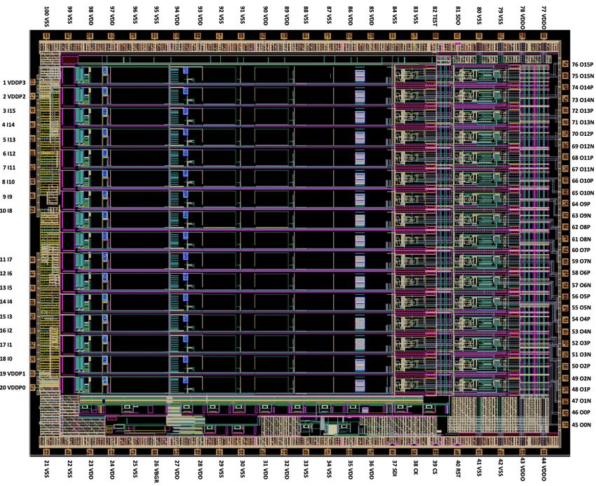
28LArASIC P5 chip-top layout status
• Disconnected RQI subtraction in CA2
• SEDC with improvements
• VOCM with down to 1kHz local filtering along with
global to improve CM noise rejection
• Replaced architecture of CMFB
• Improved pulser DAC
• Post-layout verification with new Cold models Done
from LOGIX/FNAL/LBNL
• Soft connect Vsso to Vss internally to remove body
biasing → Improve substrate noise rejection
• Vsso pads (41,42,79 and 80) are now Vss
• Top-Level DRC and LVS clean with Assura deck as
used for previous tapeouts
• Additional DRC checks being done and finalized
with latest updated DRC Calibre deck In
• Was not done before progress
• Some minor modifications needed for antenna
violation resolution (not reported with Assura)
29Summary
• P4 LArASIC identified issues well understood
• For P5 LArASIC layout:
• Disconnected RQI subtraction in CA2 → Guaranteed/Unconditional functionality at LN2 – Done
• Improved SEDC (CMFB amp modified, added CM filtering) → Stable & low-noise operation – Done
• Charge injection DAC (4 slopes matched with gains + not tied to VSS) → Improved linearity – Done
• Remove separation Vsso and Vss internally → Improved substrate noise rejection – Done
• Post-layout verification with new PSP models from LOGIX/FNAL/LBNL → Shows good performance – Done
• Top-Level DRC and LVS clean with Assura deck (used for previous tapeouts) – Done
• Additional DRC (Calibre: regular DRC, patched DRC, Antenna) checks
require minor modifications (never before recommended rules were ON) – In progress
• Submission March 3 (layout to MOSIS February 22)
30You can also read