Diffusion interface layer controlling the acceptor phase of bilayer near-infrared polymer phototransistors with ultrahigh photosensitivity - Nature
←
→
Page content transcription
If your browser does not render page correctly, please read the page content below
ARTICLE
                  https://doi.org/10.1038/s41467-022-28922-4                OPEN

                  Diffusion interface layer controlling the acceptor
                  phase of bilayer near-infrared polymer
                  phototransistors with ultrahigh photosensitivity
                  Tao Han1 ✉, Zejiang Wang1, Ning Shen1, Zewen Zhou1, Xuehua Hou2, Shufang Ding1, Chunzhi Jiang1,
                  Xiaoyi Huang1, Xiaofeng Zhang 3 ✉ & Linlin Liu2
1234567890():,;

                  The narrow bandgap of near-infrared (NIR) polymers is a major barrier to improving the
                  performance of NIR phototransistors. The existing technique for overcoming this barrier is to
                  construct a bilayer device (channel layer/bulk heterojunction (BHJ) layer). However, acceptor
                  phases of the BHJ dissolve into the channel layer and are randomly distributed by the spin-
                  coating method, resulting in turn-on voltages (Vo) and off-state dark currents remaining at a
                  high level. In this work, a diffusion interface layer is formed between the channel layer and
                  BHJ layer after treating the film transfer method (FTM)-based NIR phototransistors with
                  solvent vapor annealing (SVA). The newly formed diffusion interface layer makes it possible
                  to control the acceptor phase distribution. The performance of the FTM-based device
                  improves after SVA. Vo decreases from 26 V to zero, and the dark currents decrease by one
                  order of magnitude. The photosensitivity (Iph/Idark) increases from 22 to 1.7 × 10⁷.

                  1 Hunan Provincial Key Laboratory of Xiangnan Rare-Precious Metals Compounds Research and Application, School of Physics and Electronic Electrical
                  Engineering, Xiangnan University, Chenzhou 423000, People’s Republic of China. 2 Institute of Polymer Optoelectronic Materials and Devices, State Key
                  Laboratory of Luminescent Materials and Devices, South China University of Technology, Guangzhou 510640, People’s Republic of China. 3 National
                  Engineering Laboratory for Modern Materials Surface Engineering Technology & The Key Lab of Guangdong for Modern Surface Engineering Technology,
                  Guangdong Institute of New Materials, Guangdong Academy of Sciences, Guangzhou 510650, People’s Republic of China. ✉email: than@xnu.edu.cn;
                  zxf200808@126.com

                  NATURE COMMUNICATIONS | (2022)13:1332 | https://doi.org/10.1038/s41467-022-28922-4 | www.nature.com/naturecommunications                            1
ARTICLE NATURE COMMUNICATIONS | https://doi.org/10.1038/s41467-022-28922-4
N
ear-infrared (NIR) polymer photodetectors have attracted of noninterference bilayer films and avoids interfacial mutual dis-
extensive attention due to their potential for use in bioi- solution. However, the large distance between the acceptor phases
maging, health monitoring, and medical applications1–3. and channel layer makes it difficult to control device performance
In general, as a typical photodetector, phototransistors have by adjusting the acceptor phases in the BHJ. This issue can be
advantages over photodiodes. Phototransistors can detect light solved by employing solvent vapor annealing (SVA) treatment. The
signals that are much weaker than photodiodes because the light fullerene-based acceptor phases easily diffused during the SVA
can directly reach the active layer of the phototransistors4. treatments due to their small volume27,28. For example, Kim et al.27
At the same voltages, the dark currents of the photodiodes are fabricated high-performance bilayer organic photodiodes by con-
larger than that of the phototransistor due to the short electrode trolling donor/acceptor interdiffusion in heterojunctions sand-
distance (photodiodes: < 500 nm, phototransistors: > 5 μm)5,6. wiched between donor and acceptor layers.
However, the NIR polymer materials used in phototransistors In this work, noninterference bilayer films were prepared by
have a narrow bandgap, which always leads to a high exciton FTM. Subsequently, the FTM-based films were treated with SVA,
binding energy and the difficult dissociation of photogenerated where the acceptor phases in the BHJ were driven to the channel
excitons7. The number of photogenerated excitons in photo- transport layer. In this way, a controllable diffusion interface can
detectors is usually increased by introducing abundant acceptor be obtained. The resultant NIR phototransistors exhibited ultra-
phases8. Nevertheless, a high concentration of acceptor phases in high performance. The experimental results and possible
traditional single-layer bulk heterojunction (BHJ) photodetectors mechanism are reported below.
is needed, which can easily lead to electron/hole recombination9.
As a result, phototransistors usually have low mobility, high off-
state dark currents, and large turn-on voltages (Vo)9. Further- Results
more, the photocurrents and photosensitivity (Iph/Idark ratio) of The structure of the device consists of Si/SiO2/PDPP3T/Au/
phototransistors, which are strongly related to the shift in the PDPP3T:PC61BM (Fig. 1a), among which the FTM-based
turn-on voltages before and after illumination, decrease with an poly(diketopyrrolopyrrole-terthiophene) (PDPP3T) and PDPP
increase in Vo10. 3T:PC61BM layers were treated with SVA (chloroform solvent).
It has been reported that the design of bilayer devices (channel Figure 1b and Supplementary Fig. 1 describe the film transfer
transport layer/BHJ layer) could effectively enhance device process. The dropped solution expanded rapidly on the deio-
performance11. The channel transport layer ensures the high mobi- nized water surface to form a film. After the film was completely
lity of the bilayer devices. The BHJ layer promotes the dissociation dry, the sample was gently placed on the film surface. The
efficiency of photogenerated excitons (large photocurrents)12–16. sample was then pressed into water with tweezers but imme-
However, mutual dissolution occurs at the interface layer in the diately removed (Fig. 1b). Finally, high-quality FTM-based films
bilayer devices12,17. As a result, many randomly distributed acceptor without corner effects were obtained, and multiple samples were
phases re-enter the channel transport layer, and the performance of prepared simultaneously. This result suggested that the FTM
NIR phototransistors becomes worse11. It has been found that the could be used to prepare large-area films, thereby greatly
problem of mutual dissolution can be solved by using the poor reducing the production cost of photodetectors.
solvent of the bottom film as a good solvent for the preparation of TEM was used to observe the phase separation in the organic
the top film18 or by adding crosslinking agents into the channel blend films29. In the TEM images, PC61BM appeared dark due to
transport layer while spin-coating the second layer12. However, it is its high electron density, while PDPP3T appeared bright (Fig. 2a).
difficult to prevent the uneven distribution of acceptor phases. The The TEM images of transferred PDPP3T:PC61BM films had
degree of interfacial mutual dissolution is influenced by factors such darker areas than those of the spin-coated films (Supplementary
as the residence time of the spin-coating solution on the first layer Fig. 2). This phenomenon suggested that the separation of the
surface, spin-coating speed, and dose of solution during the pre- donor and acceptor phases in the transferred films was poorer,
paration of the second layer. which may be due to the formation of more aggregated PDPP3T
The performance of photodetectors can be improved by phases in the transferred films, thus imposing less effect on the
adjusting the acceptor phases, which act as electron capture and PC61BM phases. Additionally, the poor phase separation in the
storage units. In our previous work, the gain and response speed transferred PDPP3T:PC61BM films was also confirmed by atomic
of lateral polymer photodetectors were controlled by changing the force microscopy (AFM), as shown in Fig. 2b. More details will be
concentration of the acceptor phases19. Lateral devices with low introduced in the following section. Colberts et al.23 reported that
dark currents and fast response speeds were prepared by taking the photoactive material-based solution would spread on a water
advantage of the energy level gradient between ZnO and the substrate due to differences in surface tension (Marangoni flow).
acceptor phases20. Given the importance of the acceptors, we also The poor phase separation in the transferred PDPP3T:PC61BM
established a model to explain the electron transport mechanism. film could be attributed to the different expansion rates of the
This model was based on the electrical properties of photo- donor and acceptor phases during the spontaneous spreading of
transistors doped with different concentrations of acceptor the solution on the water surface. Despite having a low acceptor
phases21. However, to further improve and control the perfor- phase concentration, the blended films with poor phase separa-
mance of bilayer NIR photodetectors, it was found that an uneven tion could already produce an obvious light response in the
distribution of acceptor phases caused by mutual interfacial dis- phototransistors due to the existence of gate electrodes21.
solution was a major technical challenge. Therefore, the high crystallization of the PDPP3T phases formed
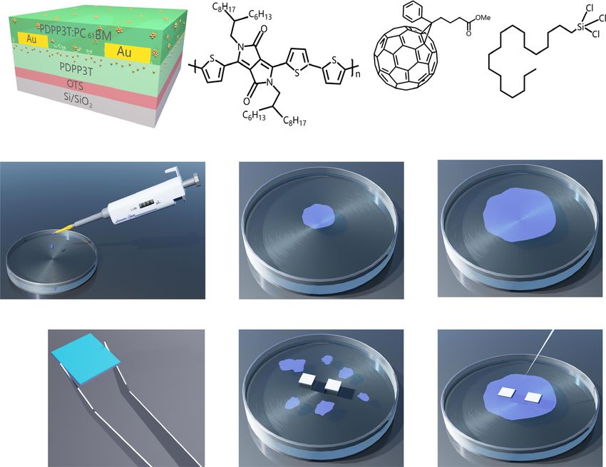
The floating film transfer method (FTM) is used to prepare in the transferred films would ensure large hole mobility, further
organic photoelectric devices. With this method, highly crystalline promoting devices with large photocurrents.
self-organized active layers with well-stacked domains are easily The absorption peak of the FTM-based PDPP3T/
formed on the water substrate via the spontaneous spreading of the PDPP3T:PC61BM bilayers showed a wide wavelength range (300-
solution22–26. For instance, Kumari et al.25 obtained air-processed 1100 nm), as shown in Fig. 2c. The absorption of the bilayers in
FTM-based organic solar cells with 13.8% efficiency. Sung et al.26 the NIR band (780-1100 nm) was significantly higher than that of
achieved high mobility FTM-based flexible organic field-effect the PDPP3T:PC61BM single layer. This increased absorption
transistors by controlling the solvent evaporation time. Using an could provide more photogenerated carriers for devices in the
FTM to prepare organic photoelectric devices enables the formation NIR band. In addition, grazing-incidence X-ray diffraction
2 NATURE COMMUNICATIONS | (2022)13:1332 | https://doi.org/10.1038/s41467-022-28922-4 | www.nature.com/naturecommunications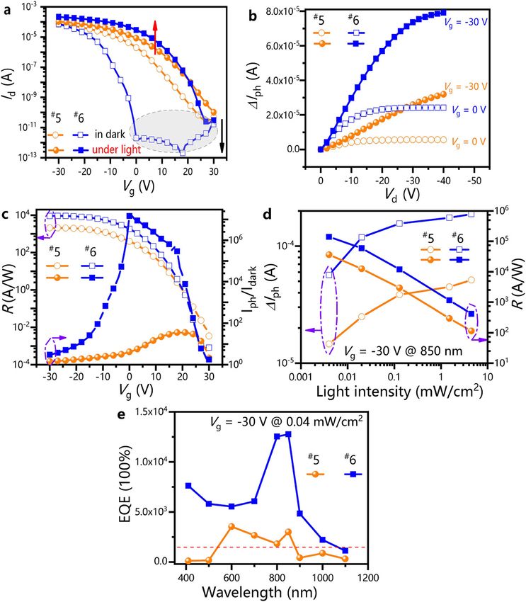
NATURE COMMUNICATIONS | https://doi.org/10.1038/s41467-022-28922-4 ARTICLE
G
6)
(3 5:9
6*66:
H
JXUVVOTM9UR[ZOUT 9UR[ZOUTYVXKGJOTM ,[RRYVXKGJOTM
IS
:XGTYLKXLORSIUSVRKZOUT )[ZZOTMZNKLORS 'JJOTMZNKYGSVRKY
Fig. 1 Device structure, molecular structures and fabrication process of the FTM-based films. a Device structure with SVA treatment and the molecular
structures of PDPP3T, PC61BM and OTS. b Schematic diagram for the fabrication of the FTM-based films.
(GIXRD) of the films showed that the donor phases in the FTM- the phenomenon observed in the PDPP3T/PDPP3T:PC61BM
based PDPP3T:PC61BM films had higher crystallinity (π-π bilayer. This result also confirmed the existence of the diffusion
packing) than the spin-coated PDPP3T:PC61BM films (Fig. 2d). process.
Deng et al.30 reported that the grain size of the organic crystals in Film depth-dependent light absorption under low-pressure
the films was remarkably enlarged via a water-surface drag oxygen plasma etching is commonly used to determine the
coating method, along with a significant improvement in the π-π interface position of films32. However, this method may drive the
packing order. Hence, FTM-based PDPP3T:PC61BM films could polymer molecules from the top layer into the bottom layer,
be used as the active layers to enhance the transport of carriers by making it difficult to distinguish weak diffusion interfaces. Hence,
optimizing the π-π stacking. Furthermore, the energy levels of in this work, the PEDOT:PSS layer was used to help measure the
PDPP3T and PC61BM were determined by ultraviolet photo- changes in the absorption peaks of PC61BM (Fig. 3c, d, Supple-
electron spectroscopy (UPS). The highest occupied molecular mentary Fig. 5). The films were treated with SVA at various
orbital (HOMO) levels were obtained from the valence band intervals and then immersed in water to remove the PEDOT:PSS/
edges (Fig. 2e) and the secondary electron cutoff (Fig. 2f), indi- PDPP3T:PC61BM layers. Afterwards, films with quartz/OTS/
cating that the HOMO levels of the PDPP3T and PC61BM were PDPP3T structures were obtained (Supplementary Fig. 5). In the
5.24 and 5.96 eV, respectively (Supplementary Table 1). The UV–Vis absorption spectra of those films, the peak intensity of
lowest unoccupied molecular orbital (LUMO) levels were deter- PC61BM increased with prolonged SVA treatment (Fig. 3c, d).
mined by combining the optical bandgap from the UV–vis This result indicated that SVA treatment promoted the diffusion
absorption spectra (Fig. 2c and Supplementary Fig. 3) with the of PC61BM into the PDPP3T channel transport layer, which also
HOMO levels. The results show that the LUMO levels of PDPP3T proved the occurrence of acceptor phase diffusion.
and PC61BM were 3.89 and 4.1 eV, respectively (Supplementary Devices with different structures were constructed to investi-
Table 1). gate the effects of the mutual dissolution interface and diffusion
In situ Raman and UV–Vis absorption spectra were obtained interface on the performance of phototransistors (Fig. 4, Sup-
to test the acceptor phase diffusion between the two FTM-based plementary Figs. 6–9, Tables 1 and 2, Supplementary Tables 2–3).
films (Fig. 3, Supplementary Figs. 4–5). For the PDPP3T/ The surface and cross-section morphologies of the bilayer films
PDPP3T:PC61BM bilayer, the Raman peak of PC61BM (at prepared by different methods are illustrated in Fig. 4d-i. The
1460 cm−1) gradually decreased with increasing SVA tempera- features of these films are described by the schematic diagram
ture (Fig. 3a–b), indicating that the acceptor phases diffused in shown in Fig. 4a–c. For the spin-coated bilayer devices, when the
the films. This observation could be explained by the fact that CHCl3-soluble PC61BM solution was used, the interface between
the volume of PC61BM was smaller than that of the PDPP3T the PDPP3T and PC61BM films was almost invisible (~184 nm,
polymer. The PC61BM phases diffused more easily after Fig. 4g), indicating that the two films had a high degree of mutual
annealing, and this diffusion followed Fick’s second low31. The dissolution. In comparison, when the THF-soluble PC61BM
in situ Raman spectra of the PDPP3T/PC61BM bilayer exhibited solution was used, a relatively blurred interface between PDPP3T
a wide variety (Supplementary Fig. 4), which was consistent with and PC61BM was observed (Fig. 4h), indicating the partial
NATURE COMMUNICATIONS | (2022)13:1332 | https://doi.org/10.1038/s41467-022-28922-4 | www.nature.com/naturecommunications 3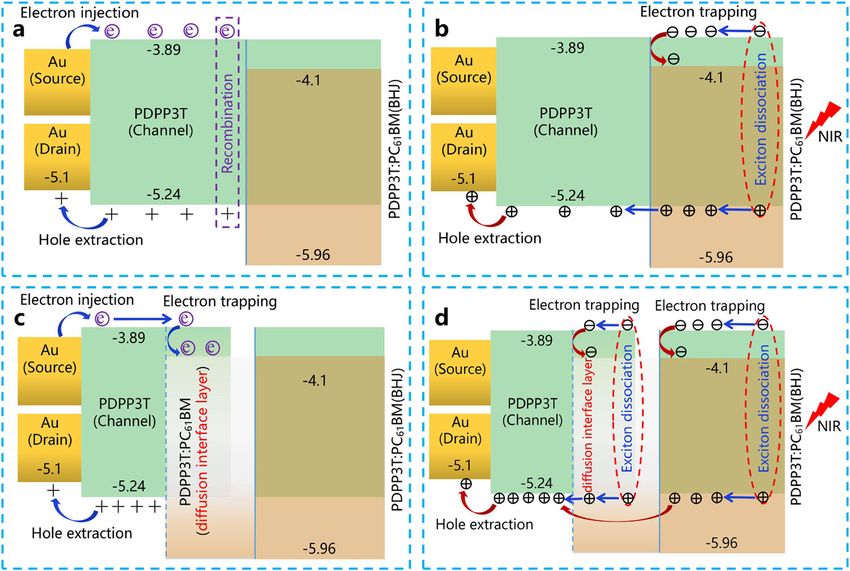
ARTICLE NATURE COMMUNICATIONS | https://doi.org/10.1038/s41467-022-28922-4
ZXGTYLKXKJ6*66: YVOTIUGZKJ6*66: 6)
(3 ZXGTYLKXKJ6*66: 6)
(3
G
H
ŦS ŦS ŦS
Fig. 2 Basic parameters of different films. a TEM. b AFM (scanning area is 2 × 2 μm2). c UV–vis absorption spectra (0-0 absorption peak at 850 nm, 0-1
absorption peak at 766 nm, 1-0 absorption peak at 334 nm). d Grazing-incidence X-ray diffraction (GIXRD) patterns. e Ultraviolet photoelectron
spectroscopy (UPS) spectra of the valence band region. f UPS spectra of the secondary electron cutoff region.
dissolution of these two films. In addition, an obvious interface bilayer device spin-coated with good solvent (Device #1: S-
was observed in the transferred bilayer devices (Fig. 4i), sug- PDPP3T/PC61BM-CHCl3) was almost identical to that of the
gesting no mutual dissolution between the first and second PDPP3T:PC61BM devices (Table 2, Supplementary Table 3). This
layers. was because the PC61BM layers spin-coated with CHCl3 could
The transferred PDPP3T devices showed a large hysteresis dissolve the bottom PDPP3T layer, forming a large mutually
window and weak light response under 850 nm illumination dissolved interface and resulting in abundant acceptor phases
(Supplementary Fig. 8a, b). The bandgap of the PDPP3T material entering the channel transport layer. However, the bilayer devices
was approximately 1.35 eV (Supplementary Table 1), and abun- spin-coated with poor solvent (Device #2: S-PDPP3T/PC61BM-
dant electrons injected from the electrode emerged in the active THF) had a thin mutual dissolution interface layer (Fig. 4b),
layers, resulting in high turn-on voltages (27 V) and off-state dark leading to the acceptor phases having a small effect on the
currents (2.0 × 10⁻⁵ μA, Supplementary Table 3). Compared with channel transport layer. Therefore, the mobility of Device #2 was
PDPP3T devices, the PDPP3T:PC61BM devices showed a stronger comparable to that of the PDPP3T devices (Supplementary Fig. 7,
light response (Supplementary Fig. 8c, d), and turn-on voltages Table 2, Supplementary Table 3). Notably, the acceptor phases
and off-state dark currents decreased simultaneously to some could capture electrons injected from the electrodes33,34, dra-
extent (Supplementary Table 3). These drops in the turn-on matically reducing the turn-on voltages (Vo ~ 1 V) of Device #2
voltages and dark currents were mainly due to electron capture by (Fig. 4j, l). When the FTM-based bilayer devices (#3 T-PDPP3T/
the acceptor phases33,34. Furthermore, the performance of the PC61BM) were prepared without SVA (Fig. 4c), no mutual
4 NATURE COMMUNICATIONS | (2022)13:1332 | https://doi.org/10.1038/s41467-022-28922-4 | www.nature.com/naturecommunications
NATURE COMMUNICATIONS | https://doi.org/10.1038/s41467-022-28922-4                                                                    ARTICLE

Fig. 3 The in situ Raman and UV–Vis absorption spectra of the FTM-based films. a In situ Raman spectra of the PDPP3T/PDPP3T:PC61BM bilayers with
SVA at different temperatures (PDPP3T-25 °C: the dark line represents the PDPP3T film at 25 °C; PDPP3T:PC61BM-25 °C: the red line represents the
PDPP3T:PC61BM film at 25 °C; PDPP3T/PDPP3T:PC61BM bilayers: the blue line represents 25 °C, the brown line represents 70 °C, the orange line
represents 80 °C, the magenta line represents 90 °C, and the deep green line represents 100 °C). b Dependence of the normalized PC61BM Raman peak in
the PDPP3T/PDPP3T:PC61BM layer on annealing temperature (data from Fig. 3a, ♣ represents the PDPP3T:PC61BM film, ♦ represents the PDPP3T film).
c Absorption spectra of the transferred films after removing the films above the PEDOT:PSS layer with different SVA times (0-0 absorption peak at
850 nm, 0-1 absorption peak at 766 nm, 1-0 absorption peak at 334 nm). d Relationship between the normalized PC61BM absorption peak and annealing
time (data from Fig. 3c).

dissolution interface was formed, so they had electrical properties             the R and Iph/Idark of the phototransistors were closely related to the
similar to those of the PDPP3T devices (Table 2, Supplementary                  gate voltages. In general, the R value of the phototransistors tended
Table 3). The effectiveness of SVA treatment on the performance                 to be large (~ 8700 A/W, Table 3) due to the photogating effect. A
of Device #4 (T-PDPP3T/PC61BM-SVA) was further tested.                          device with a high W/L value usually has a high R value. Compared
Compared with the PDPP3T devices, Device #4 showed similar                      with the W/L value of the device with an ultrahigh R value35,36, the
hole mobility and lower turn-on voltages (Vo ~ 4 V) and off-state               W/L value of our device was lower. Therefore, the increased R value
dark currents (1.8 × 10⁻⁶ μA), but higher photocurrents (33 μA)                 of the phototransistors prepared in this work might not be related
and Iph/Idark (8.3 × 10⁶) (Table 2, Supplementary Table 3,                      to the high W/L value but could be caused by the increase in the
Fig. 4j–l). These results further indicated that the acceptor phases            number of photogenerated carriers. In the dark state, the turn-on
of Device #4 diffused into the channel transport layer after SVA                voltages of the SVA devices (#6) could be reduced to almost zero by
treatment, forming a diffusion interface (Supplementary Fig. 4).                controlling the diffusion of the acceptor phases, indicating that this
Due to the formation of a diffusion interface, the electrical                   device could be used at low operating voltages. In contrast, under
properties of Device #4 were better than those of Device #2, which              illumination conditions (0.04 mW/cm2, 850 nm), the turn-on vol-
only had a thin mutually dissolved interface (Fig. 4b).                         tages of the SVA devices (#6) increased to 27 V, resulting in a large
   The FTM-based bilayer devices (PDPP3T/PDPP3T:PC61BM)                         response window (Supplementary Figs. 12–13). This significant
with diffusion interface layers exhibited superior electrical proper-           turn-on voltage shift between the dark stage and illumination state
ties in terms of the hole mobility, ΔIph, responsivity (R), Iph/Idark,          ensured that the SVA devices (#6) could be adjusted to the accu-
turn-on voltages, and EQE (Fig. 5, Supplementary Figs. 10–15,                   mulation region for illumination and to the depletion region for the
Table 3, Supplementary Table 4). The hysteresis window of the                   dark state10. The Iph/Idark value (~1.7 × 10⁷ @ Vg = 0 V, Table 3) of
FTM-based bilayer SVA devices (#6) decreased significantly, indi-                the SVA devices (#6) was significantly higher than that of the device
cating that the defects/traps in the films could be effectively elimi-           without SVA (#5). This Iph/Idark value was higher than that of the
nated (Supplementary Figs. 11–12). Hence, the hole mobility of                  NIR phototransistors reported in the literature37,38. The high Iph/
SVA devices (#6) reached 0.752 cm2·V−1·s−1 (Table 3), which was                 Idark value of our phototransistors could be attributed to the
higher than that of the PDPP3T devices (0.307 cm2·V−1·s−1,                      negative shift in the turn-on voltages. On the one hand, the dark
Supplementary Table 3). The ΔIph value of the SVA devices (#6)                  currents remained at a low level with the aid of the gate electrodes;
increased over twofold compared to that of the devices without                  on the other hand, the photocurrents increased with the negative
SVA (Vg = −30 V, Fig. 5b, Table 3), and the ΔIph value continued                shift in the turn-on voltages. In addition, the SVA devices (#6) also
to increase with light illumination (Fig. 5d). Figure 5c shows that             had high EQE (1000-13000 × 100%) in the wavelength range of

NATURE COMMUNICATIONS | (2022)13:1332 | https://doi.org/10.1038/s41467-022-28922-4 | www.nature.com/naturecommunications                             5
ARTICLE                                                                                     NATURE COMMUNICATIONS | https://doi.org/10.1038/s41467-022-28922-4

                                      G                                        J                         M

                                                                                      IS
                                          )NRUXULUXSYUR\KTZ

                                      H                                        K                         N

                                                                                      IS
                                               :.,YUR\KTZ

                                      I                                        L                          O

                                                                                      IS
                                             :XGTYLKXKJLORS

Fig. 4 Schematic diagram and electrical properties of the Si/SiO2/OTS/PDPP3T/Au/PC61BM structured devices via different fabrication methods.
a Schematic diagram of the PC61BM solution dissolved in chloroform solvent for the spin-coating bilayer device (#1 S-PDPP3T/PC61BM-CHCl3).
b Schematic diagram of the PC61BM solution dissolved in THF solvent for the spin-coating bilayer device (#2 S-PDPP3T/PC61BM-THF). c Schematic
diagram of bilayer device via FTM (#3 T-PDPP3T/PC61BM). d (#1 S-PDPP3T/PC61BM-CHCl3), e (#2 S-PDPP3T/PC61BM-THF), f (#3 T-PDPP3T/PC61BM)
Film surface photographs. g (#1 S-PDPP3T/PC61BM-CHCl3), h (#2 S-PDPP3T/PC61BM-THF), i (#3 T-PDPP3T/PC61BM) Cross-sectional SEM images of the
films (scale bar is 100 nm). j (transfer curve), k (dependence of photocurrent (ΔIph) on the source-drain voltage (Vd)), l (Vo and off-state dark current)
Electrical properties of the devices prepared by different methods. The transfer curves of the devices were measured at a constant Vd = −30 V.

 Table 1 Device structures by different preparation methodsa.

 Device                                     Dielectric layer                   First layer                          Electrode            Second layer
 #1S-PDPP3T/PC61BM-CHCl3                    SiO2 (300 nm)/OTS                  PDPP3T     (spin-coated)             Au                   PC61BM     (spin-coated with CHCl3 solvent)
 #2 S-PDPP3T/PC BM-THF                                                         PDPP3T     (spin-coated)                                  PC61BM     (spin-coated with THF solvent)
               61
 #3 T-PDPP3T/PC BM                                                             PDPP3T     (transferred)                                  PC61BM     (transferred and without SVA)
               61
 #4 T-PDPP3T/PC BM-SVA                                                         PDPP3T     (transferred)                                  PC61BM     (transferred and with SVA)
               61

 a   The thicknesses of the PDPP3T film and PDPP3T:PC61BM film via the film transfer method are 70 and 60 nm, respectively; the thickness of the PDPP3T film via the spin-coating method is 70 nm.

 Table 2 Performance parameters of the different devices.

 Device                                         ΔIph (μA)             Vo (V) in the dark               Off-state current (μA)                Mobility (cm2·V−1·s-1)                Iph/Idark
 #1S-PDPP3T/PC61BM-CHCl3                        2.3                   21                               2.1 × 10⁻⁵                            0.118                                 4
 #2 S-PDPP3T/PC BM-THF
               61                               9.6                   1                                8.0 × 10⁻⁶                            0.294                                 5.6 × 10⁵
 #3 T-PDPP3T/PC BM
               61                               8.2                   25                               1.1 × 10⁻⁵                            0.398                                 376
 #4 T-PDPP3T/PC BM-SVA
               61                               33                    4                                1.8 × 10⁻⁶                            0.336                                 8.3 × 10⁶

6                        NATURE COMMUNICATIONS | (2022)13:1332 | https://doi.org/10.1038/s41467-022-28922-4 | www.nature.com/naturecommunications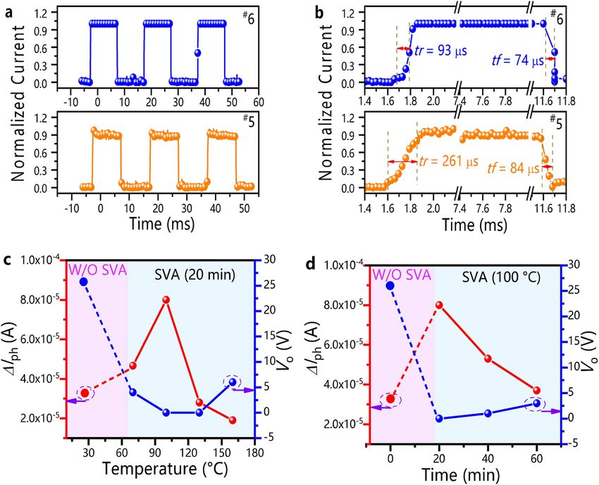
NATURE COMMUNICATIONS | https://doi.org/10.1038/s41467-022-28922-4                                                                      ARTICLE

Fig. 5 Electrical properties of devices with SVA (#6) and without SVA (#5) treatment. a Transfer curve. b Photocurrent (ΔIph) at various gate voltages.
c Dependence of R and Iph/Idark on gate voltage. d Dependence of ΔIph and R on light intensity (850 nm). e EQE spectrum at −30 V gate voltage under
illumination of 0.04 mW/cm2. The light intensity is shown in Fig. 5a–c, and Fig. 5e is 0.04 mW/cm2 @ 850 nm. The orange lines with both unfilled and
filled circles represent Device #5, and the blue lines with both unfilled and filled squares represent Device #6. The transfer curves of the devices were
measured at a constant Vd = −30 V.

 Table 3 Performance parameters of the devices with and without SVA treatment.

                  ΔIph (μA)     Vo (V) in     Off-state current    Hole mobility (cm2·V−1·s−1)       EQE       R (A/W)     Iph/Idark   tr (μs)   tf (μs)
                                the dark      (μA)
 #5 W/O    SVA    32            26            2.8 × 10⁻⁵           0.464                             3000      2000        22          261       84
 #6   With SVA    79            0             1.7 × 10⁻⁶           0.752                             13000     8700        1.7 × 10⁷   93        74

400–1100 nm (Fig. 5e, Supplementary Fig. 14b, Supplementary                     Fig. 17a, b). The above results indicated that for application as
Fig. 15b), indicating that this device could also be used as a wide             photoswitches, phototransistors had little advantage over photo-
spectral response phototransistor.                                              diodes. A dual control measurement was applied to enhance the
   The response speed of the devices before and after SVA was                   response speed of phototransistors40. With this method, the on/
tested (Fig. 6a, b, Supplementary Figs. 16–17). The long lifetime               off switching ratio was greater than 1.0 × 10⁴. The light-off
of the phototransistor carriers resulted in a slow response speed               currents were maintained at approximately 1.0 × 10⁻⁹ A (Sup-
since the turn-on voltages could hardly recover back to the initial             plementary Fig. 17d). The rise/fall times of the SVA devices (#6)
value when changing the light on/off state21,39. The on/off ratios              reached 93/74 μs (Fig. 6b). The response speed of the SVA devices
of photoswitching at various gate voltages were very small, and                 (#6) was much faster than that of the device without SVA (#5,
the light-off currents increased with increasing test time, leading             261/84 μs, Fig. 6b), which could be attributed to the fact that the
to an increase in the fall time (tf) to over 80 s (Supplementary                acceptor phases in the diffusion interface layer trapped

NATURE COMMUNICATIONS | (2022)13:1332 | https://doi.org/10.1038/s41467-022-28922-4 | www.nature.com/naturecommunications                               7
ARTICLE NATURE COMMUNICATIONS | https://doi.org/10.1038/s41467-022-28922-4 Fig. 6 Time responses and variation in electrical properties under different SVA treatment conditions. a, b Time responses via the photoelectric dual- control measurement (orange line filled with circles for Device #5, blue line with filled circles for Device #6, tr for rise time, tf for fall time). c Variation in ΔIph (red line with filled circles) and Vo (blue line with filled circles) with increasing SVA temperature (light purple area represents the device without SVA, light blue area represents the devices with SVA (20 min)). d Variation in ΔIph (red line with filled circles) and Vo (blue line with filled circles) with increasing SVA time (light purple area represents the device without SVA, light blue area represents the devices with SVA (100 °C)). The light intensity is 0.04 mW/ cm2 @ 850 nm. photogenerated electrons and accelerated the response. It is worth these carriers under two-electrode conditions (without the gate noting that the photoelectric dual control method could also be electrodes, Fig. 7). It is worth mentioning that the effect of the gate applied as switches in ultrahigh-performance logical circuits. This voltages on the photocurrents is discussed in the following session. method kept the gate voltage change and the light on/off state Figure 7 shows the energy level diagram to analyse the effects of change at the same frequency, improving the response speed and the diffusion interface layer on the increase in device performance. stability of the switches. The use of this dual-control method also The energy levels of the PDPP3T and PC61BM materials illu- enabled organic materials with low mobility to be applied in logic strated in this diagram were obtained by analyzing UPS and circuits that required a large on/off switching ratio, fast response absorption spectra (Supplementary Table 1). For the SVA-free speed and high stability. devices in the dark state (Fig. 7a), the electrons could be con- The acceptor phases in the diffusion interface layer could be tinuously injected from the gold electrodes into the channel controlled by changing the time interval and temperature of the transport layer, and a large number of electrons were generated41. SVA treatments (Fig. 6c, d, Supplementary Figs. 11–12, Supple- During device operation, the recombination of electrons and holes mentary Figs. 18–19). For example, with increasing SVA tem- would result in a large hysteresis window, high off-state dark perature, the turn-on voltages of the devices first decreased and currents, and turn-on voltages42, which would adversely affect then increased. However, the values were still significantly lower device performance (Supplementary Fig. 11b). However, for the than the turn-on voltages of the devices without SVA (Fig. 6c). In devices with SVA in the dark state, the electrons injected by the addition, the trend of the device performance with extension of electrode could transfer to the acceptor phases in the diffusion the SVA time is similar to that with the SVA temperature change interface layer (Fig. 7c). Therefore, the channel transport layer (Fig. 6d). Combined with the information illustrated in Fig. 3 and would not be affected by the electrons, resulting in devices with a Supplementary Figs. 4–5, it could be found that increasing the slight hysteresis window, small off-state dark currents and turn-on SVA temperature and extending the SVA time promoted the voltages, and high mobility (Supplementary Fig. 12b, Tables 2 and diffusion of more acceptor phases. Hence, diffusion interface 3). According to Fig. 7b and d, when the devices were exposed to layers with different thicknesses were formed, which ensured that light, photogenerated electrons in the active layer would be cap- the Vo value of the devices with SVA treatment under different tured by the acceptor phases, while the photogenerated holes conditions was lower than that of the devices without SVA. would transfer to the channel transport layer for transmission. The performance of devices treated with SVA was better than Moreover, the diffusion interface layer of the devices with SVA those treated without SVA due to the existence of the diffusion would also generate photogenerated carriers, resulting in addi- interface layer. This phenomenon could be explained by the tional photocurrents (Fig. 5b, d). As a result, the photogenerated movement of the photogenerated carriers. For this purpose, the currents, Iph/Idark ratios, and response of the devices with SVA simplified physical model was used to illustrate the movement of were greater than those of the devices without SVA (Table 3). 8 NATURE COMMUNICATIONS | (2022)13:1332 | https://doi.org/10.1038/s41467-022-28922-4 | www.nature.com/naturecommunications
NATURE COMMUNICATIONS | https://doi.org/10.1038/s41467-022-28922-4                                                                              ARTICLE

Fig. 7 Energy level diagram of the different devices. a Device without SVA in the dark state. b Device without SVA under illumination. c Device with SVA
in the dark state. d Device with SVA under illumination.

   Based on the analysis of the carrier movement under the                      an ultrahigh Iph/Idark value of 1.7 × 10⁷, a small turn-on voltage of
condition of two electrodes (Fig. 7), the effects of gate voltages              0 V, and a fast response speed of 93/74 μs. A diffusion interface
were discussed to explore the photogating/amplification effects on               layer, instead of a mutual dissolution interface layer, was formed
the performance of the phototransistors (Supplementary                          between the channel transport layer and bulk heterojunction layer
Figs. 20–21). When phototransistors are in the turn-off state, the              to prevent the random distribution of acceptor phases. The
photocurrents usually increase linearly with increasing light                   acceptor phases in the diffusion interface could trap the electrons
intensity due to the photoconductivity effect prevalent in                      injected by the electrode in the dark state and supply additional
photodiodes43,44. In comparison, when phototransistors are in                   photocurrents when illuminated. Thus, the off-state dark currents
the turn-on state, the photovoltaic effect is significant (Eq. 4)                decreased by one order of magnitude, and the photocurrents
since the photovoltage is induced by the accumulation of trapped                increased over twofold. This novel device structure was con-
electrons43. It can be seen that the photocurrents varied in the                structed by combining FTM with an SVA treatment. This strategy
devices with SVA (#6) and without SVA treatment (#5). The                       is expected to be widely used for composite systems that dissolve
photocurrents exhibited a nonlinear relationship with the light                 well in solvents with low boiling points. The novel device structure
intensity in the turn-on state (Vg = −30 V, Supplementary                       proposed in this work has promising applicability for fabricating
Figs. 20–21), which satisfied Eq. (4). Therefore, the transcon-                  high-performance and low-cost phototransistors.
ductance (GM) values of the devices were calculated to estimate
the photogating/amplification effect. Due to the formation of a                  Methods
diffusion interface in devices (#6) after SVA treatment, the GM                 Materials. Octadecyltrichlorosilane (OTS, 98%), isopropanol (99%), tetra-
value of devices (#6) was 5.3 μS under weak light, which was                    hydrofuran (THF, 99%) and o-dichlorobenzene (ODCB, 99%) were all purchased
lower than that in the devices without SVA (#5). The smaller GM                 from J&K Scientific. CHCl3 (99.8%) and PC61BM were purchased from
value in Device #6 could be attributed to the occurrence of a large             Sigma–Aldrich and 1-Material, respectively. Poly{2,20-[(2,5-bis(2-hexyldecyl)-3,6-
                                                                                dioxo-2,3,5,6-tetrahydropyrrolo[3,4-c]pyrrole-1,4-diyl)dithiophene]-5,50-diyl-alt-
drift in the threshold voltages under weak light (Fig. 5a and                   thiophen-2,5-diyl} (PDPP3T), indaceno[1,2-b:5,6-b’]dithiophene-co-2,1,3-ben-
Table 3). The GM values of the SVA devices (#6) increased slowly                zothiadiazole (IDT-BT), poly(3-hexylthiophene-2,5-diyl) (P3HT) and PEDOT:PSS
with increasing light intensity from 5.3 to 6.7 μS. In contrast, the            were purchased from Solarmer Materials. None of the commercially available
GM value decreased from 7.3 to 4.3 μS in devices without SVA                    chemicals were further purified. In the first layer, high n-doped silicon was used as
                                                                                the back-gate dielectric, and thermally grown SiO2 (300 nm) was selected as the
(#5). According to Fig. 7, the diffusion interface of the SVA                   inorganic gate dielectric.
devices (#6) provided an additional donor/acceptor interface to
separate photogenerated carriers. As a result, under strong light,
                                                                                Device fabrication. Both the Si/SiO2 substrates and the OTS (30 μL) were placed
the photocurrents of the SVA devices (#6) were difficult to reach a              in a petri dish covered by aluminum foil and heated on a hot plate (140 °C, two
saturated state (Supplementary Table 5), resulting in an increas-               hours) in a nitrogen environment. The self-assembled OTS layer was prepared after
ing GM value (Supplementary Fig. 21b). The advantages of the                    cleaning the extra OTS off the substrates by spin-coating a CHCl3 solution (100 μL,
diffusion interface layer were highlighted by comparing the                     6000 rpm, 60 s). The PDPP3T (0.2 wt%) and PDPP3T:PC61BM (0.2 wt%) solutions
                                                                                used for spin-coating were dissolved in mixed solvents of ODCB and CHCl3
changes in the GM value of the two devices.                                     (volume ratio = 4:1)45. All the solutions were stirred for over 12 hours at 100 °C.
                                                                                PC61BM (1 wt%) was dissolved in CHCl3 and THF, and the PC61BM layer was
                                                                                spin-coated at a speed of 2000 rpm for 60 s. The PDPP3T layer (70 nm) was spin-
Discussion                                                                      coated in two steps (700 rpm for 10 s and 1200 rpm for 60 s), and the
                                                                                PDPP3T:PC61BM layer (60 nm) was spin-coated at 1200 rpm for 60 s. Both the
In this research, a broad spectral response (400–1100 nm) of NIR                PDPP3T and PDPP3T:PC61BM layers were vacuum annealed at 100 °C (10 min) to
polymer phototransistors with high EQEs (1000–13000 × 100%)                     eliminate trapping and obtain a uniform phase orientation in the film. The
was achieved. In addition, the prepared phototransistors exhibited              PEDOT:PSS layer (20 nm) used to test the acceptor absorption peak was spin-

NATURE COMMUNICATIONS | (2022)13:1332 | https://doi.org/10.1038/s41467-022-28922-4 | www.nature.com/naturecommunications                                         9
ARTICLE NATURE COMMUNICATIONS | https://doi.org/10.1038/s41467-022-28922-4
coated (2000 rpm, 60 s) in a solution diluted with 50% isopropanol. The source and The phototransistors satisfy the photovoltaic effect in the turn-on state, which
drain electrodes of the device were prepared by thermally evaporating a Au film satisfies the following equation43:
(50 nm). The devices with SVA treatment were placed in a petri dish (30 μL
CHCl3) covered by aluminum foil and then annealed in a nitrogen glove box. ΔI ph ¼ GM ΔV th ð4Þ
where GM is the transconductance and ΔVth is the shift in the turn-on voltage.
In situ Raman spectra. Si/SiO2/OTS was used as the substrate, and the active layer
was selected (PDPP3T, PC61BM, PDPP3T:PC61BM, PDPP3T/PC61BM and Data availability
PDPP3T/PDPP3T:PC61BM) to prepare related samples. The Raman test data at the Source data for Fig. 2c–f, Fig. 3, Fig. 4j–l, Figs. 5 and 6, Tables 1–3, Supplementary Figs. 3
same depth were selected for in situ Raman characterization of the samples
and 4, Supplementary Figs. 6–9, Supplementary Figs. 11 and 12, Supplementary
annealed at different temperatures. PDPP3T-25 °C, PC61BM-25 °C and
Figs. 14–21 and Supplementary Tables 1–5 are provided as a source data file. Source data
PDPP3T:PC61BM-25 °C were tested at 25 °C, and the PDPP3T/PC61BM and
are provided with this paper.
PDPP3T/PDPP3T:PC61BM films were tested under annealing conditions of
25–130 °C and 25–100 °C, respectively. The variation in the characteristic Raman
peak of PC61BM at 1460 cm-1 was chosen to analyse the effect of annealing on Received: 7 August 2021; Accepted: 14 February 2022;
PC61BM.
FTM. In terms of the devices prepared by FTM, CHCl3 (low boiling point) was used
as the solvent for the PDPP3T (0.2 wt%), IDT-BT (0.25 wt%), PC61BM (1 wt%),
P3HT (0.25%) and PDPP3T:PC61BM (0.2 wt%) solutions. All these solutions were
stirred over 12 h at 90 °C. During the film transfer process, an organic solution References
within 30 μL was dropped into a petri dish filled with deionized water. The com- 1. Huang, J. et al. A high-performance solution-processed organic photodetector
pletely transferred film was vacuumed for more than 20 min to remove excess water for near-infrared sensing. Adv. Mater. 32, 1906027 (2020).
vapor. The PDPP3T and PDPP3T:PC61BM films were annealed in a glove box at 2. Chow, P. C. Y. & Someya, T. Organic photodetectors for next-generation
100 °C in a nitrogen atmosphere for 10 min. wearable electronics. Adv. Mater. 32, 1902045 (2020).
The whole FTM process was recorded as a video and added to this work in 3. Wang, C., Zhang, X. & Hu, W. Organic photodiodes and phototransistors
Supplementary Movie 1. Moreover, a series of high-quality films were successfully toward infrared detection: materials, devices, and applications. Chem. Soc. Rev.
prepared via FTM (Supplementary Fig. 22), such as PDPP3T, IDT-BT,
49, 653–670 (2020).
PDPP3T:PC61BM, and P3HT films. Among all these films, the quality of the
4. Han, T. et al. Lateral polymer photodetectors using silver nanoparticles
PC61BM film with a smaller molecular weight was slightly poor. In addition,
promoted PffBT4T-2OD:PC61BM composite. ACS Photonics 5, 4650–4659
devices of different sizes could be fabricated by FTM. Taking the IDT-BT film as an
(2018).
example, the transferred film still showed high quality even though the device size
was increased to 8 × 9 cm2 (Supplementary Fig. 23c). A large-area flexible film 5. Wang, H. & Kim, D. H. Perovskite-based photodetectors: materials and
could also be obtained via FTM (Supplementary Fig. 23b). These results indicated devices. Chem. Soc. Rev. 46, 5204–5236 (2017).
that the preparation of high-quality films via FTM was scalable and promising. 6. Guo, F. et al. A nanocomposite ultraviolet photodetector based on interfacial
trap-controlled charge injection. Nat. Nanotechnol. 7, 798–802 (2012).
7. Li, N., Lan, Z., Cai, L. & Zhu, F. Advances in solution-processable near-
Photodetector characterization. The measurements of the film thicknesses and infrared phototransistors. J. Mater. Chem. C. 7, 3711–3729 (2019).
absorption spectra (UV–vis) were performed with a Dektak 150 instrument 8. Wadsworth, A., Hamid, Z., Kosco, J., Gasparini, N. & McCulloch, I. The bulk
(Veeco) and Shimadzu UV-3100 spectrophotometer, respectively. The films were heterojunction in organic photovoltaic, photodetector, and photocatalytic
observed by atomic force microscopy (AFM), transmission electron microscopy applications. Adv. Mater. 32, 2001763 (2020).
(TEM), and scanning electron microscopy (SEM) with a Dimension edge instru- 9. Han, H. et al. Strong composition effects in all-polymer phototransistors with
ment (Bruker), JEOL-2100F instrument (JEOL), and Sigma 300 instrument (Zeiss), bulk heterojunction layers of p-type and n-type conjugated polymers. ACS
respectively. The in situ Raman spectra and film surface photographs were
Appl. Mater. Inter. 9, 628–635 (2017).
obtained using an inVia Reflex instrument (Renishaw) and P40 Pro instrument
10. Shou, M. et al. Ultrahigh detectivity in spatially separated hole/electron dual
(HUAWEI), respectively. Ultraviolet photoelectron spectroscopy (UPS) measure-
traps based near-infrared organic phototransistor. Adv. Opt. Mater. 9,
ments were carried out with a Nexsa (Thermo Fisher) system using a He(I)
2002031 (2021).
excitation energy of 21.22 eV. The grazing incidence X-ray diffraction (GIXRD)
was investigated by a Smart Lab III instrument (Rigaku). The electrical perfor- 11. Gao, Y. et al. A novel hybrid‐layered organic phototransistor enables efficient
mance of the phototransistors was recorded in air using a four-semiconductor intermolecular charge transfer and carrier transport for ultrasensitive
parameter analyser (Keithley 2636B) with a Cascade probe station. During the photodetection. Adv. Mater. 31, 1900763 (2019).
photoelectric dual-control measurement40, the response time at the microsecond 12. Li, Q. et al. High-performance near-infrared polymeric phototransistors
level was measured by a digital storage oscilloscope (2012B, Tektronix) combined realized by combining cross-linked polymeric semiconductors and bulk
with a lock-in amplifier (LIA-MV-150, Femto). Light illumination at different heterojunction bilayer structures. Appl. Mater. Today 22, 100899 (2021).
wavelengths (410–2400 nm, 20 Hz) was provided by a continuous spectrum light 13. Kim, H., Wu, Z., Eedugurala, N., Azoulay, J. D. & Ng, T. N. Solution-
source (Opolette 355 LD), where the light intensity was tested by a laser power processed phototransistors combining organic absorber and charge
meter (header Ophir NOVA II and probe PD300-UV). transporting oxide for visible to infrared light detection. ACS Appl. Mater.
Inter. 11, 36880 (2019).
14. Lim, D. H. et al. Unsymmetrical small molecules for broad-band
Displayed equations. In the dark state, the device mobility (μ) is calculated
photoresponse and efficient charge transport in organic phototransistors. ACS
according to the following equation46:
Appl. Mater. Inter. 12, 25066–25074 (2020).
pffiffiffiffi!2 15. Huang, F. et al. Broadband organic phototransistor with high photoresponse
2L ∂ Id from ultraviolet to near-infrared realized via synergistic effect of trilayer
μ¼ ð1Þ
WCi ∂V g heterostructure. J. Mater. Chem. C. 6, 8804–8811 (2018).
16. Han, J. et al. Graphene/organic semiconductor heterojunction
where L (40 μm) is the channel length, W (1000 μm) is the channel width, Id is the phototransistors with broadband and bi-directional photoresponse. Adv.
source-drain current, Vg is the gate voltage. And Ci (11.5 nF/cm2) is the capaci- Mater. 30, 1804020 (2018).
tance per unit area of the SiO2 dielectric caused by the negligible capacitance of the 17. Dong, S. et al. High‐performance large‐area organic solar cells enabled by
self-assembled OTS monolayer. sequential bilayer processing via nonhalogenated solvents. Adv. Energy Mater.
In addition, the responsivity (R) and the external quantum efficiency (EQE, 9, 1802832 (2019).
where the value is equal to (G) of a photodetector can be characterized by the 18. Zhong, Z. et al. Dark current reduction strategy via a layer-by-layer solution
following equation2,47: process for a high-performance all-polymer photodetector. ACS Appl. Mater.
Inter. 11, 8350–8356 (2019).
ΔI Ph 19. Shou, M. et al. Simultaneous photomultiplication improvement and response
R¼ ð2Þ
Pinc acceleration for high-performance lateral polymer photodetectors based on
bulk heterojunction. ACS Appl. Mater. Inter. 13, 5293–5301 (2021).
20. Han, T. et al. Energy level gradient trapping based on different work functions
hυ
EQE ¼ R ´ ´ 100% ð3Þ of ZnO enhancing response and stablity for lateral photodetectors. Org.
q Electron. 86, 105883 (2020).
21. Han, T. et al. The mechanism of photogenerated minority carrier movement
where ΔIph is the photocurrent, Pinc is the incident light power, h is the Planck
in organic phototransistors. J. Mater. Chem. C. 8, 12284–12290 (2020).
constant, υ is the frequency of light, and q is the absolute value of electron charge.
10 NATURE COMMUNICATIONS | (2022)13:1332 | https://doi.org/10.1038/s41467-022-28922-4 | www.nature.com/naturecommunicationsNATURE COMMUNICATIONS | https://doi.org/10.1038/s41467-022-28922-4 ARTICLE
22. Noh, J., Jeong, S. & Lee, J. Y. Ultrafast formation of air-processable and high- 46. Zaumseil, J. & Sirringhaus, H. Electron and ambipolar transport in organic
quality polymer films on an aqueous substrate. Nat. Commun. 7, 1–9 (2016). field-effect transistors. Chem. Rev. 107, 1296–1323 (2007).
23. Colberts, F. J. M. et al. Bilayer-ternary polymer solar cells fabricated using 47. Li, C. et al. Ultrafast and broadband photodetectors based on a perovskite/
spontaneous spreading on water. Adv. Energy Mater. 8, 1802197 (2018). organic bulk heterojunction for large-dynamic-range imaging. Light-Sci. Appl
24. Sun, L., Jiang, X. & Zhou, Y. Efficient nonfullerene organic solar cells with 9, 1–8 (2020).
active layers fabricated by water transfer printing. J. Energy Chem. 37, 220–224
(2019).
25. Kumari, T. et al. Over 13.8% efficiency of organic solar cells fabricated by air- Acknowledgements
processable spontaneously spreading process through water temperature T.H. acknowleges support form the Hunan Provincial Natural Science Foundation of
control. Nano Energy 85, 105982 (2021). China (2019JJ50565), Scientific Research Fund of Hunan Provincial Education
26. Sung, Y. et al. Flexible bottom-gated organic field-effect transistors utilizing Department (18A461), Scientific Research Fund of Chenzhou (zdyf201908), Fund of
stamped polymer layers from the surface of water. ACS Appl. Mater. Inter. 12, Xiangnan University (2019XJ29), the Scientific Research Start-up Fund for High-level
25092–25099 (2020). Talents in Xiangnan University, 2020 National Innovation and Entrepreneurship
27. Kim, H., Song, B., Lee, K., Forrest, S. & Kanicki, J. Bilayer interdiffused Training Program for College Students (S202010545034). The work of X.F.Z. is
heterojunction organic photodiodes fabricated by double transfer stamping. supported by the Natural Science Foundation of China (51801034, 52172067), and the
Adv. Opt. Mater. 5, 1600784 (2017). Guangdong Province Outstanding Youth Foundation (2021B1515020038). The work
28. Chen, D., Liu, F., Wang, C., Nakahara, A. & Russell, T. P. Bulk heterojunction of L.L. is supported by the Natural Science Foundation of China (51873068,
photovoltaic active layers via bilayer interdiffusion. Nano Lett. 11, 2071–2078 51573055).
(2011).
29. Choi, Y. et al. Optimized phase separation in low-bandgap polymer:fullerene Author contributions
bulk heterojunction solar cells with criteria of solvent additives. Nano Energy T.H. and X.Z. conceived the idea and supervised the project. Z.W., N.S. and Z.Z. fab-
30, 200–207 (2016). ricated the device and carried out optoelectronic characterizations. X.H. and L.L. con-
30. Deng, W. et al. Water-surface drag coating: a nNew route toward high-quality tributed to the in-situ Raman tests and analysis. S.D. contributed to the response speed
conjugated small-molecule thin films with enhanced charge transport characterizations. C.J. and X.H. proposed the meschanism of the device. T.H. and X.Z.
properties. Adv. Mater. 33, 2005915 (2021). interpreted the results and wrote the manuscript.
31. Watts, B. et al. A quantitative study of PCBM diffusion during annealing of
P3HT:PCBM blend films. Macromolecules 42, 8392–8397 (2009).
32. He, S. et al. Vertical miscibility of bulk heterojunction films contributes to Competing interests
high photovoltaic performance. Adv. Mater. Interfaces 7, 2000577 (2020). The authors declare no competing interests.
33. Zhao, Z., Li, C., Shen, L., Zhang, X. & Zhang, F. Photomultiplication type
organic photodetectors based on electron tunneling injection. Nanoscale 12,
1091–1099 (2020).
Additional information
Supplementary information The online version contains supplementary material
34. Miao, J. & Zhang, F. Recent progress on photomultiplication type organic
available at https://doi.org/10.1038/s41467-022-28922-4.
photodetectors. Laser Photonics Rev. 13, 1800204 (2019).
35. Guo, Y. et al. High-performance phototransistors based on organic
Correspondence and requests for materials should be addressed to Tao Han or Xiaofeng
microribbons prepared by a solution self-assembly process. Adv. Funct. Mater.
Zhang.
20, 1019–1024 (2010).
36. Chow, P. C. Y. et al. Dual-gate organic phototransistor with high-gain and
Peer review information Nature Communications thanks Felix Dollinger and the other,
linear photoresponse. Nat. Commun. 9, 1–8 (2018).
anonymous, reviewer(s) for their contribution to the peer review of this work. Peer
37. Li, F. et al. High-performance near-infrared phototransistor based on n-type
reviewer reports are available.
small-molecular organic semiconductor. Adv. Electron. Mater. 3, 1600430 (2016).
38. Li, D. et al. Flexible and air‐stable near‐infrared sensors based on solution‐
Reprints and permission information is available at http://www.nature.com/reprints
processed inorganic-organic hybrid phototransistors. Adv. Funct. Mater. 31,
2105887 (2021). Publisher’s note Springer Nature remains neutral with regard to jurisdictional claims in
39. Jin, Z. et al. Bilayer heterostructured PThTPTI/WS2 photodetectors with high published maps and institutional affiliations.
thermal stability in ambient environment. ACS Appl. Mater. Inter. 8,
33043–33050 (2016).
40. Han, T. et al. Ultrahigh photosensitive organic phototransistors by
photoelectric dual control. J. Mater. Chem. C. 7, 4725–4732 (2019). Open Access This article is licensed under a Creative Commons
41. Simone, G., Dyson, M. J., Meskers, S. C. J., Janssen, R. A. J. & Gelinck, G. H. Attribution 4.0 International License, which permits use, sharing,
Organic photodetectors and their application in large area and flexible image adaptation, distribution and reproduction in any medium or format, as long as you give
sensors: the role of dark current. Adv. Funct. Mater. 30, 1904205 (2020). appropriate credit to the original author(s) and the source, provide a link to the Creative
42. Park, B., Choi, S., Graham, S. & Reichmanis, E. Memory and photovoltaic Commons license, and indicate if changes were made. The images or other third party
elements in organic field effect transistors with donor/acceptor planar-hetero material in this article are included in the article’s Creative Commons license, unless
junction interfaces. J. Phys. Chem. C. 116, 9390–9397 (2012). indicated otherwise in a credit line to the material. If material is not included in the
43. Noh, Y.-Y. et al. Effect of light irradiation on the characteristics of organic article’s Creative Commons license and your intended use is not permitted by statutory
field-effect transistors. J. Appl. Phys. 100, 094501 (2006). regulation or exceeds the permitted use, you will need to obtain permission directly from
44. Fuentes-Hernandez, C. et al. Large-area low-noise flexible organic the copyright holder. To view a copy of this license, visit http://creativecommons.org/
photodiodes for detecting faint visible light. Science 370, 698–701 (2020). licenses/by/4.0/.
45. Ye, L. et al. From binary to ternary solvent: morphology fine-tuning of D/A
blends in PDPP3T-based polymer solar cells. Adv. Mater. 24, 6335–6341
(2012). © The Author(s) 2022
NATURE COMMUNICATIONS | (2022)13:1332 | https://doi.org/10.1038/s41467-022-28922-4 | www.nature.com/naturecommunications 11You can also read