Nanodomain structure of single crystalline nickel oxide - Nature
←
→
Page content transcription
If your browser does not render page correctly, please read the page content below
www.nature.com/scientificreports
OPEN Nanodomain structure of single
crystalline nickel oxide
B. Walls1*, A. A. Mazilkin2, B. O. Mukhamedov3, A. Ionov2, I. A. Smirnova2,
A. V. Ponomareva3, K. Fleischer4, N. A. Kozlovskaya3, D. A. Shulyatev3, I. A. Abrikosov5*,
I. V. Shvets1 & S. I. Bozhko2
In this work we present a comprehensive study of the domain structure of a nickel oxide single crystal
grown by floating zone melting and suggest a correlation between point defects and the observed
domain structure. The properties and structure of domains dictate the dynamics of resistive switching,
water splitting and gas sensing, to name but a few. Investigating the correlation between point
defects and domain structure can provide a deeper understanding of their formation and structure,
which potentially allows one to tailor domain structure and the dynamics of the aforementioned
applications. A range of inhomogeneities are observed by diffraction and microscopy techniques.
X-ray and low-energy electron diffraction reveal domains on the submicron- and nanometer-
scales, respectively. In turn, these domains are visualised by atomic force and scanning tunneling
microscopy (STM), respectively. A comprehensive transmission electron microscopy (TEM) study
reveals inhomogeneities ranging from domains of varying size, misorientation of domains, variation
of the lattice constant and bending of lattice planes. X-ray photoelectron spectroscopy and electron
energy-loss spectroscopy indicate the crystal is Ni deficient. Density functional theory calculations—
considering the spatial and electronic disturbance induced by the favourable nickel vacancy—reveal
a nanoscale distortion comparable to STM and TEM observations. The different inhomogeneities are
understood in terms of the structural relaxation induced by ordering of nickel vacancies, which is
predicted to be favourable.
Metal oxides display a wide variety of physical properties, stimulating interest from the point of view of fun-
damental physics and device engineering. NiO is antiferromagnetic and a charge transfer insulator. However,
nickel vacancies are common and give rise to an effective p-type d oping1. NiO sees application in spin v alves2,
supercapacitors3, hole transport layer in perovskite solar c ells4, water splitting (Fe doped NiO)5 and gas sensing6.
Floating zone melting (FZM) is one of the most suitable techniques for the growth of high quality metal oxide
single crystals (for detailed review s ee7,8). Despite the high quality of single crystals grown by FZM, different
types of structural and chemical inhomogeneities can exist. Crystal lattice defects in FZM single crystals such as
domain boundaries, dislocation walls, twins and stacking faults affect the structure of X-ray diffraction (XRD)
reflexes9. Lab based X-ray sources can probe the coherent domain size and overall crystalline quality10,11 but
cannot easily distinguish between or study particular two-dimensional defects. The standard statistical approach
of X-ray diffractometry allows one to obtain information averaged over ensembles in the kinematical12,13, semi-
dynamical14 or dynamical approaches15. However, comprehensive investigation of crystal structure requires the
combination of methods providing statistically averaged information and high spatial resolution electron and
scanning probe microscopy techniques. Point defects are considered to be scattered homogeneously throughout
the crystal and appear in diffraction spectra as a background signal with the reflex structure unaffected. Con-
sequently, even high-quality single crystals, as judged by diffraction techniques, can contain a relatively high
concentration of point defects.
The macroscopic properties of most metal oxides are extremely sensitive to the presence of point defects.
Focusing on monoxides, cation vacancies can induce fascinating properties such as ferromagnetism in the case
of CoO16 and half-metallicity in the case of MnO17, CoO18 and NiO17. In the latter, single defects can produce
half-metallicity in either spin channel locally. However, the interaction of vacancies resulting in half-metallicity
1
School of Physics and Centre for Research on Adaptive Nanostructures and Nanodevices (CRANN), Trinity
College Dublin, Dublin 2, Ireland. 2Institute of Solid State Physics, Russian Academy of Sciences, Chernogolovka,
Russia. 3Materials Modeling and Development Laboratory, NUST MISIS, Leninskiy prosp, 4, Moscow,
Russia 199049. 4School of Physical Sciences, Dublin City University, Dublin 9, Ireland. 5Department of Physics,
Chemistry and Biology (IFM), Linköping University, 58183 Linköping, Sweden. *email: wallsbc@tcd.ie;
igor.abrikosov@liu.s
Scientific Reports | (2021) 11:3496 | https://doi.org/10.1038/s41598-021-82070-1 1
Vol.:(0123456789)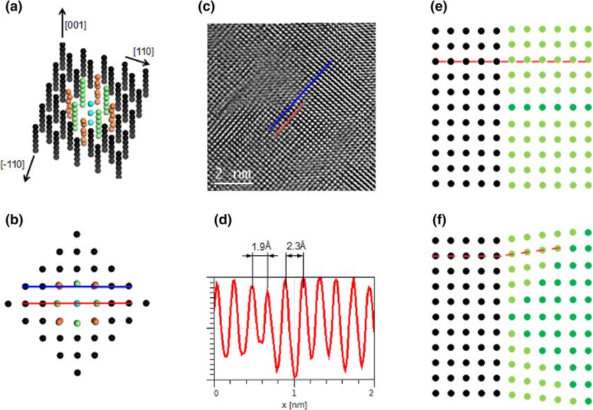
www.nature.com/scientificreports/
(c) 108
1.00E+08 Rocking Curve
(a)
107
1.00E+07
Counts
2θ (o)
106
1.00E+06
1.00E+05
105
2.5 o
1.00E+04
104
20
20 21 22 23 24 25
incident angle (o) incident angle (o)
109
1.00E+09
(b) θ/2θ scan (d)
1.00E+08
108
incident angle (o)
2θ: 43.52o
1.00E+07
107
FWHM:
Counts
0.078o
1.00E+06
106
1.00E+05
105
1.00E+04
104
43 43.5 44
2θ (o) sample posi
on (mm)
Figure 1. (a) Reciprocal space map shown in terms of incident angle and 2θ angle. (b) shows the θ/2θ scan for
the NiO single crystal obtained by summing all the columns of the reciprocal space map. The average coherent
domain size is estimated to be 115 ± 2 nm. (c) shows the corresponding rocking curve derived from summing
all the rows of the reciprocal space map. The indicated angular interval shows that there are misoriented areas
within the probed sample volume. (d) Rocking curves as a function of sample position. The sample was moved
by 0.5 mm per step. The misorientation of the domain is maintained over the probed region. The dotted line
indicates the region of the sample where (a–c) have been taken.
in the same spin channel is predicted to be energetically f avourable19. Nickel oxide’s antiferromagentic order
is predicted to persist even in the presence of the cation vacancy and resulting half-metallicity17. The resistive
switching observed in a variety of metal oxides including N iO20–23 appears to be due to intrinsic point defects.
These defects produce states at various levels within the band gap, which are likely responsible for transport
within the insulator.
Larger-scale structural inhomogeneities are known to strongly influence physical phenomena and applica-
tions. For example, electric field induced conductive filaments in NiO films form predominately at domain
boundaries19,24,25. Therefore, boundary density and structure dictate the resistive switching properties. The gas
sensing and water splitting performance of metal oxides is also strongly correlated to domain s ize26–28.
Therefore, studying domain structure and how vacancies can dictate domain structure is vital. In this work
we reveal a complex domain structure of a NiO single crystal and demonstrate that it can be correlated to point
defects. Diffraction techniques reveal both submicron- and nanometer-scale domains, which are visualised by
microscopy techniques. Electron energy-loss spectroscopy (EELS) and X-ray photoelectron spectroscopy (XPS)
reveal a Ni deficiency and density functional theory (DFT) calculations demonstrate the Ni vacancy induces a
nanometer-scale distortion. Analysis of these measurements and calculations allow us to propose a correlation
between the point defects and the domains of different size.
Results
Experimental results. The domain structure of the FZM grown NiO single crystal has been examined
in detail by XRD measurements of the [002] r eflex29, depicted in Fig. 1. The lattice constant is estimated to be
4.154 ± 0.004 Å, comparable to the reported value of 4.17Å30,31. The reciprocal space map (RSM) is depicted in
Fig. 1a. Figure 1b shows the θ/2θ scan obtained by summing all the columns of the RSM. The misorientation of
local regions of the crystal leads to a broadening of the reflex in 2θ . This is due to the mosaic structure of the
crystal and the deformation of the crystal locally. Using the Scherrer equation we can estimate the average coher-
ent domain size to be 115 ± 2 nm. The corresponding rocking curves, derived by summing all the rows of the
RSM, is presented in Fig. 1c. The analysed spot size is 1 × 5 mm and within the XRD scattering volume we see
two distinct reflexes separated by an angular offset of around 2 ◦ . We have to stress that in symmetric XRD scans
we are not directly sensitive to the lateral domain size but rather towards the columnar structure normal to the
crystal surface. Taking rocking curves at several areas of the sample in 0.5 mm steps (see Fig. 1d) reveals that the
tilt of the domains is maintained over the probed region. Please note that due to the line focus we can only map
Scientific Reports | (2021) 11:3496 | https://doi.org/10.1038/s41598-021-82070-1 2
Vol:.(1234567890)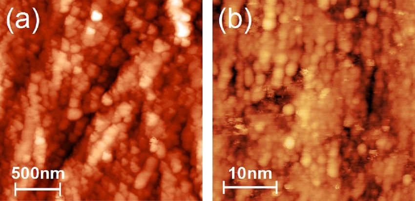
www.nature.com/scientificreports/
Figure 2. (a) AFM image (2.5 × 2.5 µm2 ) of the NiO(001) surface and (b) STM image (30 × 30 nm2 ) of the
Ni1−xLix O (001) surface. The domains are around 100 nm and several nanometers in size in AFM and STM
images, respectively.
Figure 3. LEED of (a) Ni1−xLixO(001) and (b) NiO(001) surfaces after ion etching and annealing. (a)
E = 45 eV and (b) E = 115 eV. From the width of the spot profile in (a) the coherent area size is estimated to be
d = 6–8 nm.
in one direction. Intensities are also not directly proportional to the volume of the domains as angular optimisa-
tion in the second tilt direction was only performed on one specific misorientation.
A tapping mode atomic force microscopy (AFM) measurement of the crystal is presented in Fig. 2a. Features
of around 100 nm are observed, consistent with the coherent domain size observed in XRD. Clusters of spherical
domains have been observed on cobalt doped NiO single crystalline fi lms32: the average particle size was found
to vary between 108 and 156 nm, comparable to this work.
In Fig. 2b a scanning tunneling microscope (STM) image of a Li doped NiO single crystal is presented. The
measurement has been performed on a doped crystal as the undoped crystal was not sufficiently conductive for
STM measurements. The doped crystal has been grown by the same method as the updoped crystal and XPS
measurements estimate a Li dopant concentration of 0.4 ± 0.1% (See Supplementary Fig. S3 online). Similarly to
the undoped crystal, the Ni1−xLix O single crystal’s domain structure has also been examined in detail by XRD:
it is comparable to the undoped crystal and is discussed in the Supplementary Information (Supplementary
Fig. S1 online). Prior to the constant-current mode STM measurement the doped crystal has been subjected to
multiple sputter anneal cycles (see Methods section below). The STM image demonstrates that in addition to the
submicron-scale domains observed by XRD, nanodomains are present. The nanodomains have a typical size of a
few nanometers. The local corrugation between adjacent nanodomains of up to a nanometer cannot be purely an
electronic effect, and hence, the contrast reflects the topography of the surface. This nanodomain structure could
not be removed or changed by ion etching and annealing in ultra-high vacuum, which indicates the structure is
not due to contamination or random disorder but is inherent to the bulk of the crystal.
A low-energy electron diffraction (LEED) measurement of the doped crystal—obtained immediately after
the STM measurement—is depicted in Fig. 3a. The undoped crystal has been subjected to the identical sputter-
anneal treatment and its LEED pattern is presented in Fig. 3b. The cubic reciprocal space unit cells correspond
to the (001) surface of NiO. In both cases the lattice constant is estimated to be 4.3 ± 0.2 Å. Note the quality
of the diffraction patterns after ion etching and annealing, illustrating the crystallographic correlation of the
nanodomains. Estimation of the coherent area size from the width of the LEED spots gives a value of 6–8 nm for
the doped and undoped crystals. The nanodomain structure of the undoped NiO crystal is examined in detail
by TEM below. However, the STM and LEED measurements suggests nanodomains exist at the surface. This is
critical to gas sensing and water splitting26–28.
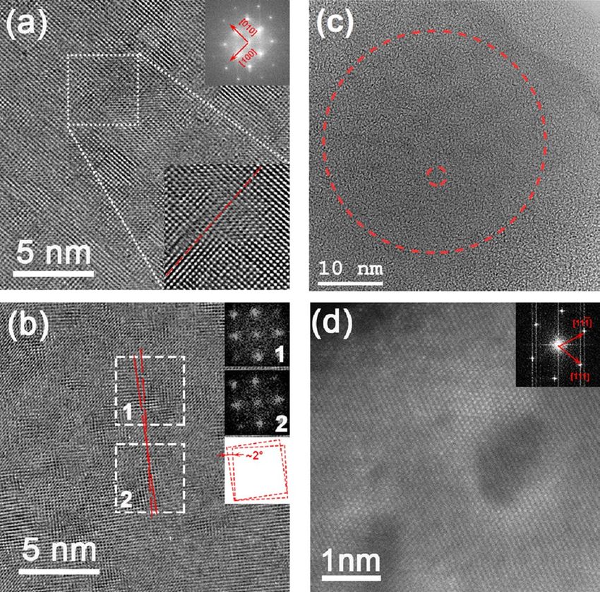
Figure 4a–c depicts high-resolution transmission electron microscopy (HR TEM) images of the NiO crystal
with the electron beam parallel to [001] NiO direction. TEM measurements estimate the lattice constant to be
4.08 ± 0.05 Å. A specific feature of the TEM images is the non-uniformity of the contrast. Linear features along
Scientific Reports | (2021) 11:3496 | https://doi.org/10.1038/s41598-021-82070-1 3
Vol.:(0123456789)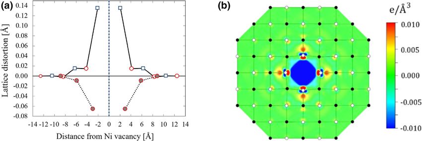
www.nature.com/scientificreports/

                                            Figure 4.  (a–c) HR TEM image of the NiO single crystal; sample normal is parallel to the [001] direction. (a)
                                            Structure contains linear features in two perpendicular directions marked by arrows. Reflection blurring in the
                                            corresponding FFT (inset top) can indicate the domain structure of the NiO crystal. The FFT filtered portion
                                            of the image is enlarged in the bottom right inset. The bending of a lattice fringe is highlighted by the dashed
                                            red line, which serves as an eye-guide. (b) Small scale HR TEM image reveals the presence of the crystalline
                                            domains. Two FFTs from neighbouring areas 1 and 2 demonstrate in-plane lattice rotation of approximately 2 ◦
                                            that is shown schematically by two red misoriented squares. Two red dashed lines in (b) serve as an eye-guide
                                            to demonstrate the in-plane domain rotation. Disturbance of atomic resolution contrast confirms the out-of-
                                            plane lattice rotation. (c) The small dashed circle highlights an example of a small domain, similar in size to
                                            those visualised in (a), which agglomerate to form a larger feature (large circle). (d) HR STEM HAADF image.
                                            Electron beam is parallel to [110] NiO direction. Contrast indicates regions attributed to different nickel density.

                                            the perpendicular [100] and [010] crystallographic directions in Fig. 4a are evident. The image indicates that
                                            the NiO crystal is split into ∼ 2–3 nm cells. Some of these cells are perfectly oriented along the [001] zone axis
                                            showing atomically resolved contrast, while the neighbouring cells are misaligned with lattice fringes visible
                                            only in the [100] or [010] direction. The presence of the misoriented areas is also supported by the fast Fourier
                                            transform (FFT), where the blurring of the lattice reflections is observed. This nanoscale inhomogeneity justifies
                                            the domain structure revealed by STM. The enlarged portion of the HR TEM image (Fig. 4a bottom inset) also
                                            reveals the bending of a lattice fringe highlighted by the dashed red line; atomic columns are shifted in the mid-
                                            dle part of the line. The presence of nano-scale cells in the NiO single crystalline sample is also shown in Fig. 4b.
                                            The two FFTs, which both correspond to the (002) plane, reveal the two regions are (001) orientated. However,
                                            the orientation of the local (200) lattice fringes differ. This is highlighted by the two non-parallel red lines and
                                            the comparison of the FFTs. Hence, the cells are aligned with respect to the surface normal but misaligned in the
                                            surface plane by an angle of around 2 ◦ (see the schematics in the insert). The disturbance of atomic resolution
                                            contrast in particular areas confirms the out-of-plane lattice rotation. The few degrees misorientation of the NiO
                                            domains observed by HR TEM is in accordance with the XRD measurements. In Fig. 4c the submicron-scale
                                            domain (big circle) appears to be an aggregation of nanodomains (small circle). The size of the former and the
                                            latter are on the same scale as the features observed in AFM and STM measurements, respectively. This infers a
                                            correlation between the domains observed on the nano- and submicron-scale.
                                                We also performed TEM measurements with the electron beam parallel to [110] NiO direction. Figure 4d
                                            is the STEM high angle annular dark field (HAADF) image. Here we observe areas with darker contrast, both
                                            equiaxial and elongated, from one to several nanometers in size. In the case of elongated areas, their larger axis
                                            lies close to the [100] crystallographic direction. From this image, we can conclude that these nanodomains
                                            are located in the (001) plane of the NiO crystal. Usually the contrast in a STEM HAADF image is correlated
                                            to the atomic number of the elements by the power law, ∼ Z1.8 (Z-contrast). Therefore, the contrast in Fig. 4d
                                            is correlated to the density of Ni ions, while the oxygen is not visible due to its lower atomic number. However,
                                            we should note that HR STEM is more sensitive to local sample orientation than HR TEM. As a result, we can
                                            interpret the low-contrast areas in Fig. 4d as nanodomains misoriented with respect to the adjacent area. In this
                                            case, when the local orientation is deviated from the zone axis, it is difficult to separate domain misorientation
                                            from Ni content. Although one should note that nickel content and misorientation can be inherently linked.
                                                EELS estimation of the NiO elemental composition—depicted in the Supplementary Information (Supple-
                                            mentary Fig. S2 online)—demonstrates a small deficiency of Ni cations. EELS measurements were performed
                                            on multiple locations (5 different samples and around 10 measurements for each sample), and every time we

          Scientific Reports |   (2021) 11:3496 |                https://doi.org/10.1038/s41598-021-82070-1                                                    4

Vol:.(1234567890)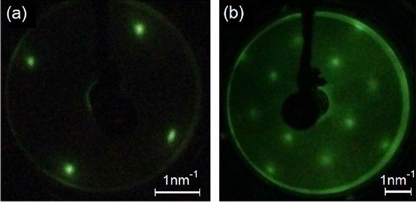
www.nature.com/scientificreports/
Property Theory (this work) Experiment
Lattice parameter, Å 4.17 4.1730,37
Magnetic moment, µb 1.815 1.930, 1.7738
Band gap, eV 4.0 4.237, 4.339, 4.040
Table 1. Calculated properties of bulk NiO and available experimental data.
Figure 5. (a) Lattice distortion induced by a charged Ni vacancy (VNi2−). Distortions along [100] and [110]
crystallographic axes are plotted with solid and dotted lines, respectively. Circles and squares denote Ni and
O atoms, respectively. Positive and negative values of the lattice distortions indicate an outward and inward
deformations, respectively. (b) Charge density difference induced by the Ni vacancy (VNi2−) in the (001) plane.
Negative (blue colour) and positive (red colour) corresponds to a reduction or an increase of the charge density
compared to the bulk cell, respectively.
calculated a Ni deficiency. Statistically the Ni deficit was about 2% (48:52). XPS measurements (Supplementary
Fig. S3 online) of the sputtered surface shows only the presence of Ni and O peaks with very small peaks attrib-
uted to argon and carbon. The atomic ratio of Ni to O was estimated to be 48:52 (2% deficit of Ni). The accuracy
of XPS quantification is about 1–1.5% (details are presented in the Supplementary Information). To preserve the
overall electrical neutrality in a NiO crystal with a Ni deficit, some Ni2+ is converted to Ni3+. The Ni3+ ions were
also detected by XPS. The observation of nickel deficiency is not surprising; NiO is a p-type semiconductor in
normal growth c onditions1. In equilibrium defect chemistry, NiO usually has a nickel deficiency accommodated
by nickel v acancies33,34. The Ni vacancy formation energy is low in comparison with the O vacancy formation
energy35. Due to the relative error of both the EELS and XPS measurements we cannot quantitatively determine
the Ni content. However, considering the XPS and EELS measurements and the above considerations we strongly
suggest the NiO crystal is Ni deficient and this deficiency is due to nickel vacancies. The non-stoichiometry
indicates the point defects and the inhomogeneity they create locally may be correlated to the observed domain
structure. In order to investigate this we have performed DFT calculations examining the spatial and electronic
disturbance of a nickel vacancy.
Density functional theory calculations. One way to treat systems with strong correlations like NiO
is an implementation of a Hubbard Coulomb term U and exchange parameter J into DFT framework36. We
have tested the GGA+U method with different values of Ueff (Ueff = U − J ) and compared the calculated band
gap, lattice parameter and magnetic moment with experiment. Table 1 compares the calculated properties with
available experimental data for U = 9 eV and J = 1 eV, i.e. Ueff = 8 eV. Our theoretical results on the lattice
parameter, on-site magnetic moment and band gap agree well with experimental data from30,37–40, which pro-
vides confidence in the chosen values of U and J parameters for the Ni atoms. The predicted lattice parameter is
4.17Å. For comparison, in this work we estimate the lattice constant to be 4.154 ± 0.004 Å, 4.08 ± 0.05 Å and
4.3 ± 0.2 Å by XRD, TEM and LEED, respectively.
For simulating the effects from a Ni vacancy, we used a supercell approach where each lattice vector of the
rhombohedral unit cell was expanded three times, i.e. 3 × 3 × 3 supercell containing 432 ions in total. According
to35, the 2- charge state of the Ni vacancy is the most stable vacancy configuration in the wide range of Fermi
level. Following that work, we use the same vacancy configuration (VNi2−) in our calculations. Figure 5a shows
the lattice distortions along the [100] and [110] crystallographic directions induced by a single nickel vacancy
VNi2−. Deformation along {111} directions are not shown due to the comparably small size. The vacancy induces
an outward shift of the oxygen atoms along {100} crystallographic directions: the nearest oxygen atoms move
away from the defect site by 0.14 Å. At the same time, along {110} directions the vacancy produces an inward
shift: the nearest nickel atoms move towards the centre of the vacancy by 0.06 Å. This behaviour can be explained
by electrostatic interaction between the charged vacancy and surrounding ions: negatively charged V Ni2− repels
Scientific Reports | (2021) 11:3496 | https://doi.org/10.1038/s41598-021-82070-1 5
Vol.:(0123456789)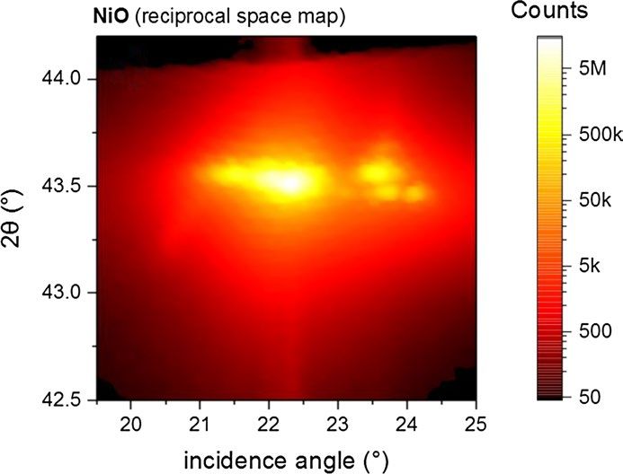
www.nature.com/scientificreports/
Figure 6. (a,b) Model containing a sequence of nickel vacancies along the [001] direction. Vacancies are within
the blue column. The columns which experience significant relaxation due to the vacancies are depicted in green
and orange. The relaxation—taken from the DFT calculation—is visualised in (b), which is a (001) plane. Red
and blue lines in (b) illustrate the variation in the lattice constant and the bending of a lattice fringe induced by
the vacancies. These predicted inhomogeneities are comparable to experiment; In (c) the blue line highlights
an example of the bending of a lattice fringe, while (d) is the line profile corresponding to the red line in (c)
and illustrates the variation in the lattice constant. (e) The dark green row represents a line (or plane out of the
page) containing ordered nickel vacancies. The relaxation of adjacent rows (or planes) results in the decoherence
of the light green and black regions, similar to an edge dislocation highlighted by the red-dashed line. (f) The
triangular network of vacancies results in the light green and black regions being misorientated with respect to
each other, highlighted by the red-dashed lines.
oxygen anions and attracts nickel cations. The size of the distorted region is about 1.3 nm in diameter, which
compares to the average size of nanodomains observed in STM.
In Fig. 5b we show the charge density difference induced by the V Ni2− vacancy. It was calculated as a differ-
ence in charge density between the vacancy-containing supercell and the bulk supercell. However, in the bulk
supercell we created the similar lattice distortions as in the vacancy-containing supercell. In Fig. 5b, one can see
a distribution of defect states in real space. As expected, the vacancy site has a negative charge. The defect states
exhibit a mixture of 3d–Ni and 2p–O states, though the latter dominates. The defect state is spread over a distance
∼ 4.7 Å, although slight excitations can be observed on oxygen atoms at the distance of 6.25 Å away from the
vacancy centre. This result also agrees qualitatively with our STM and TEM observations of the nanodomains.
Discussion
Park et al. have investigated point defects in NiO and the interaction between them19. Certain VNi–VNi arrange-
ments are strongly favoured over the non-interacting case. Specifically, nickel vacancies separated by around
8 Å along {001} directions is the favourable configuration. This is in agreement with asymmetric nanodomains
presented in the HR STEM HAADF image (Fig. 4d), which are located in (001) plane and elongated in the [100]
crystallographic direction of the NiO crystal.
We now hypothesise how the range of observed inhomogeneities are correlated to the ordering of nickel
vacancies. Figure 6a,b depicts a model containing several nickel vacancies separated by around 8 Å along the
[001] direction. The atomic positions in the vicinity of the vacancies correspond to that of the fully relaxed DFT
calculation. In Fig. 6a the atomic column containing vacancies is depicted in blue and the nearest and second-
nearest parallel atomic columns are directed by green and orange, respectively. The relaxation in the vicinity
of the vacancies is evident in (b), which is a top down view of (a). The red line in (b) illustrates the predicted
variation of the lattice constant induced by the vacancies. This can be compared to the variation in the lattice
constant observed by TEM; Fig. 6c shows the HR TEM image of the NiO crystal and (d) is a line profile cor-
responding to the red line in the TEM image. The local variation in the lattice constant is evident. The blue line
Scientific Reports | (2021) 11:3496 | https://doi.org/10.1038/s41598-021-82070-1 6
Vol:.(1234567890)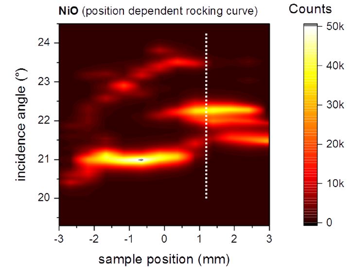
www.nature.com/scientificreports/
in (b) illustrates how the vacancy network can give rise to the bending of a lattice fringe, which is comparable
to the observed bending in TEM measurements, highlighted by the blue line in (c). Note the structure the TEM
line profiles pass through are perfectly oriented along the [001] zone axis showing atomic resolved contrast.
Therefore, the inhomogeneities in this area cannot be understood in terms of an isolated vacancy or randomly
distributed vacancies. A one-dimensional row of vacancies along the [001] direction—predicted to be the favour-
able vacancy configuration—can give rise to the observed one-dimensional inhomogeneities. The nanodomain
observed in STEM HAADF is suggested to be in the (001) plane of the NiO crystal. Within the nickel vacancy
ordering picture, this domain can consist of two-dimensional network of vacancies within the (001) plane. Small
domains, similar in size to those visualised in Fig. 4a, agglomerate due to interdomain interaction to form a
larger features, which are visualised in AFM.
Figure 6e,f illustrates schematically how the ordered vacancies can produce lattice decoherence. The dark
green in (e) illustrates a line (or plane perpendicular to the page) network of vacancies. The relaxation results
in a shift of the adjacent atomic columns (or planes). As a result the light green region is shifted with respect to
the black region. This is similar to an edge dislocation. If we consider a larger network of vacancies, such as the
triangular network depicted in (f), one can visualise how the clustering of vacancies can result in the misorienta-
tion of regions (black and light green in schematic).
The presence of nanodomain structure has also been observed in the superconducting oxide YBCO with
a orthorhombic structure41. In comparison to this work, the nanostructure inhomogeneity was attributed to
nonstoichiometry.
Conclusions
Different types of inhomogeneities in a range of submicron- to nanometer-scale are observed by a range of dif-
fraction and microscopy techniques. The diffraction measurements illustrate the quality of the crystal but also a
domain structure; XRD reveals domains of around 100 nm misoriented by several degrees, while LEED estimates
domains of around 10 nm. AFM and STM image structures on the same length scale as XRD and LEED. In
addition, TEM reveal structural inhomogeneity in the form of variation of the lattice constant, misorientation
of domains and the bending of lattice planes. Finally, TEM reveals that nanodomains agglomerate into a larger
submicron-scale structure.
The nature of the atomic-scale domain structure is studied using ab initio simulations. The distortion induced
by a nickel vacancy is examined. This is the energetically favourable point defect and the reduced Ni/O ratio,
observed by EELS and XPS, indicate its presence in the crystal. The DFT+U calculations reveal the spatial extent
of the distorted area around the Ni vacancy is approximately 1.2 nm, close to that observed by TEM and STM. The
defect state shows the same spatial distribution. The distance between overlapping defects is therefore 1.2 nm or
less. Ordering of Ni vacancies is predicted to be favourable19. It is suggested that clustering of vacancies can give
rise to formation of the range of inhomogeneities, the nature of which depends of the cluster size and structure.
As such, the defects of different size, from atomic- to submicron-scale, are coupled.
Methods
NiO and Ni1−xLix O single crystals were grown by non-crucible FZM. Rods for FZM were prepared from high
purity NiO and Li2CO3 . The initial materials were weighed to the desired ratio, pressed into cylindrical rods and
fired in air at 1100 ◦ C for 8 h. The sintered rods were float zone melted in ambient conditions at a growth rate of
10–12 mm/h. As a result both lithium doped (∼ 1%) and undoped NiO single crystals, 35–40 mm in length and
3–4 mm in diameter, were obtained. Disk-shaped samples of 1 mm thickness and 4 mm diameter were prepared
by cutting the cylindrical rods. The crystallographic orientation was controlled by back-Laue scattering, such
that the surface normal of the disk was oriented along the [001] direction.
The AFM image was obtained with a Solver PROM from NT MDT. The images were obtained in tapping
mode. The STM used in this work was a commercial slider-type STM from Createc. The images presented were
obtained in constant-current mode at room temperature. The STM tip used was [001]-oriented single-crystalline
tungsten, which was electrochemically etched in NaOH. The bias is applied to the sample with respect to the
tip. LEED measurements have been performed in the same ultra-high vacuum chamber. In order to obtain a
clean and ordered surface prior to in situ LEED and STM measurements, the surface was cleaned in situ by
sputtering with argon ions for 1 h at each 3 kV, 2 kV, 1 kV and 0.5 kV in an argon partial pressure of 10−5 mbar.
After each iteration of sputtering the crystal was annealed in vacuum at 600 ◦ C for 1 h. The sample temperature
was estimated with a K-type thermocouple. The crystal was then exposed to atmospheric conditions to recover
the oxygen content and subsequently annealed in situ at 600 ◦ C in 20 min intervals until a sharp (1 × 1) LEED
pattern was obtained.
XRD patterns have been measured with a Bruker D8 Discovery using a Cu-Kα source. Crystal orientation
was obtained using Bruker’s EVA program.
The samples for the TEM investigations were prepared on VERSA 3D HighVac dual beam facility (FEI) using
the Ga ion beam. Regular FIB lamella preparation was carried out at 30 kV and followed by 2 kV final step to
improve the surface quality. TEM investigations were performed on Titan 80-300 (FEI) transmission electron
microscope equipped with GIF (Gatan) for the EELS study. The EEL spectra were collected at the convergence
and collection angles of 14 and 15 mrad correspondingly, and with a spectral resolution of 0.2 eV/ch. For the
EEL spectra quantification the background was fitted within an energy window of ∼ 50 eV with a power-law
function. The sample thickness was less than the mean free path so the procedure of multiple inelastic scattering
deconvolution was not performed. The intensity beyond the edge onset was integrated over a window of 70 eV
to minimize the influence of the corresponding near-edge fine structure. The setup for HR STEM imaging was a
50 µm C2 aperture, convergence angle of 10 mrad, camera length of 195 mm and collection angle 30–180 mrad.
Scientific Reports | (2021) 11:3496 | https://doi.org/10.1038/s41598-021-82070-1 7
Vol.:(0123456789)www.nature.com/scientificreports/
First-principles electronic structure calculations of NiO were performed using the projector augmented wave
(PAW) method42 implemented in Vienna ab initio simulation package (VASP)43–45. The exchange-correlation
effects were treated using the spin-polarised generalised gradient approximation46 in combination with the Hub-
bard Coulomb term (GGA + U) according to the Dudarev scheme37. Below the Néel temperature, NiO exhibits
type-II antiferromagnetic order. In calculations the magnetic properties were accounted for within the collinear
picture. The magnitude and orientations of the collinear local moments were calculated self-consistently. The
cut-off energy for plane waves was set to 500 eV. The integration over the irreducible part of Brillouin zone has
been carried out using the Monkhorst–Pack m ethod47 on grids of 6 × 6 × 6 k-points. The convergence criterion
for electronic subsystem was 10 eV for subsequent iterations. The relaxation of atomic positions was realised by
−4
calculating the Hellman–Feynman f orces48,49 and stress tensor using the conjugated gradient method. Relaxation
was stopped when the forces became on the order of 5 × 10⁻³ eV/Å.
Received: 17 September 2020; Accepted: 30 December 2020
References
1. Khler, J. Transition metal oxides. An introduction to their electronic structure and properties. Angew. Chem. 105, 477. https://doi.
org/10.1002/ange.19931050352 (1993).
2. Vardimon, R., Klionsky, M. & Tal, O. Indication of complete spin filtering in atomic-scale nickel oxide. Nano Lett. 15, 3894–3898.
https://doi.org/10.1021/acs.nanolett.5b00729 (2015).
3. Cao, C.-Y., Guo, W., Cui, Z.-M., Song, W.-G. & Cai, W. Microwave-assisted gas/liquid interfacial synthesis of flowerlike NiO hollow
nanosphere precursors and their application as supercapacitor electrodes. J. Mater. Chem. 21, 3204. https://doi.org/10.1039/c0jm0
3749d(2011).
4. Aydin, E. et al. Room-temperature-sputtered nanocrystalline nickel oxide as hole transport layer for p-i-n perovskite solar cells.
ACS Appl. Energy Mater. 1, 6227–6233. https://doi.org/10.1021/acsaem.8b01263 (2018).
5. Fominykh, K. et al. Iron-doped nickel oxide nanocrystals as highly efficient electrocatalysts for alkaline water splitting. ACS Nano
9, 5180–5188. https://doi.org/10.1021/acsnano.5b00520 (2015).
6. Soleimanpour, A. M., Jayatissa, A. H. & Sumanasekera, G. Surface and gas sensing properties of nanocrystalline nickel oxide thin
films. Appl. Surf. Sci. 276, 291–297. https://doi.org/10.1016/j.apsusc.2013.03.085 (2013).
7. Shulyatev, D., Karabashev, S., Arsenov, A. & Mukovskii, Y. Growth and investigation of doped rare earth manganite single crystals.
J. Cryst. Growth 198–199, 511–515. https://doi.org/10.1016/s0022-0248(98)01146-4 (1999).
8. Koohpayeh, S. M., Fort, D. & Abell, J. S. The optical floating zone technique: a review of experimental procedures with special
reference to oxides. Prog. Cryst. Growth Charact. Mater. 54, 121–137. https://doi.org/10.1016/j.pcrysgrow.2008.06.001 (2008).
9. Shpak, A. P. et al. Combined double- and triple-crystal X-ray diffractometry with account for real defect structures in all crystals
of X-ray optical schemes. Phys. Status Solidi (a) 204, 2651–2656. https://doi.org/10.1002/pssa.200675700 (2007).
10. Fewster, P. F. Reciprocal space mapping. Crit. Rev. Solid State Mater. Sci. 22, 69–110. https://doi.org/10.1080/10408439708241259
(1997).
11. Bozhko, S., Glebovsky, V., Semenov, V. & Smirnova, I. On the growth of tungsten single crystals of high structural quality. J. Cryst.
Growth 311, 1–6. https://doi.org/10.1016/j.jcrysgro.2008.09.175 (2008).
12. Dederichs, P. H. Diffuse scattering from defect clusters near Bragg reflections. Phys. Rev. B 4, 1041–1050. https://doi.org/10.1103/
physrevb.4.1041 (1971).
13. Krivoglaz, M. A. Distribution of the scattering intensity. General aspects. In X-Ray and Neutron Diffraction in Non-ideal Crystals,
1–73 (Springer, Berlin, 1996). https://doi.org/10.1007/978-3-642-74291-0_1.
14. Molodkin, V. B., Olikhovskii, S. I., Dmitriev, S. V., Nizkova, A. I. & Lizunov, V. V. Dynamical effects in the integrated X-ray scat-
tering intensity from imperfect crystals in Bragg diffraction geometry. I. Semi-dynamical model. Acta Crystallogr. Sect. A Found.
Adv. 76, 45–54. https://doi.org/10.1107/s2053273319014281 (2020).
15. Pavlov, K. M. & Punegov, V. I. Statistical dynamical theory of X-ray diffraction in the Bragg case: application to triple-crystal dif-
fractometry. Acta Crystallogr. Sect. A Found. Crystallogr. 56, 227–234. https://doi.org/10.1107/s0108767399016694 (2000).
16. Negi, D. S. et al. Robust room temperature ferromagnetism in epitaxial CoO thin film. Appl. Phys. Lett. 103, 242407. https://doi.
org/10.1063/1.4847775 (2013).
17. Ködderitzsch, D., Hergert, W., Szotek, Z. & Temmerman, W. M. Vacancy-induced half-metallicity in MnO and NiO. Phys. Rev. B
68, 125114. https://doi.org/10.1103/physrevb.68.125114 (2003).
18. Negi, D. S., Datta, R. & Rusz, J. Defect driven spin state transition and the existence of half-metallicity in CoO. J. Phys. Condens.
Matter 31, 115602. https://doi.org/10.1088/1361-648x/aafd11 (2019).
19. Park, S. et al. Interaction and ordering of vacancy defects in NiO. Phys. Rev. B 77, 134103. https: //doi.org/10.1103/physre vb.77.13410
3 (2008).
20. Bruyere, J. C. & Chakraverty, B. K. Switching and negative resistance in thin films of nickle oxide. Appl. Phys. Lett. 16, 40–43. https
://doi.org/10.1063/1.1653024 (1970).
21. Jung, K. et al. Temperature dependence of high- and low-resistance bistable states in polycrystalline NiO films. Appl. Phys. Lett.
90, 052104. https://doi.org/10.1063/1.2437668 (2007).
22. Seo, S. et al. Reproducible resistance switching in polycrystalline NiO films. Appl. Phys. Lett. 85, 5655–5657. https://doi.
org/10.1063/1.1831560 (2004).
23. Kim, D. C. et al. Electrical observations of filamentary conductions for the resistive memory switching in NiO films. Appl. Phys.
Lett. 88, 202102. https://doi.org/10.1063/1.2204649 (2006).
24. Kawai, M., Ito, K., Ichikawa, N. & Shimakawa, Y. Thermally formed conducting filaments in a single-crystalline NiO thin film.
Appl. Phys. Lett. 96, 072106. https://doi.org/10.1063/1.3309709 (2010).
25. Park, G.-S. et al. Observation of electric-field induced Ni filament channels in polycrystalline NiO x film. Appl. Phys. Lett. 91,
222103. https://doi.org/10.1063/1.2813617 (2007).
26. Korotcenkov, G., Han, S.-D., Cho, B. K. & Brinzari, V. Grain size effects in sensor response of nanostructured SnO2- and In2O3-based
conductometric thin film gas sensor. Crit. Rev. Solid State Mater. Sci. 34, 1–17. https: //doi.org/10.1080/104084 30902 81572 5 (2009).
27. Rothschild, A. & Komem, Y. The effect of grain size on the sensitivity of nanocrystalline metal-oxide gas sensors. J. Appl. Phys. 95,
6374–6380. https://doi.org/10.1063/1.1728314 (2004).
28. Gupta, N. M. Factors affecting the efficiency of a water splitting photocatalyst: a perspective. Renew. Sustain. Energy Rev. 71,
585–601. https://doi.org/10.1016/j.rser.2016.12.086 (2017).
Scientific Reports | (2021) 11:3496 | https://doi.org/10.1038/s41598-021-82070-1 8
Vol:.(1234567890)www.nature.com/scientificreports/
29. Sasaki, S., Fujino, K. & Takéuchi, Y. X-ray determination of electron-density distributions in oxides, MgO, MnO, CoO, and NiO,
and atomic scattering factors of their constituent atoms. Proc. Jpn. Acad. Ser. B Phys. Biol. Sci. 55, 43–48. https://doi.org/10.2183/
pjab.55.43 (1979).
30. Cheetham, A. K. & Hope, D. A. O. Magnetic ordering and exchange effects in the antiferromagnetic solid solutions Mn x Ni1−x O.
Phys. Rev. B 27, 6964–6967. https://doi.org/10.1103/physrevb.27.6964 (1983).
31. Cairns, R. W. & Ott, E. X-ray studies of the system nickel–oxygen–water. I. Nickelous oxide and hydroxide. J. Am. Chem. Soc. 55,
527–533. https://doi.org/10.1021/ja01329a013 (1933).
32. Sharma, R. et al. Effect of cobalt doping on microstructural and optical properties of nickel oxide thin films. Mater. Sci. Semicond.
Process. 23, 42–49. https://doi.org/10.1016/j.mssp.2014.02.004 (2014).
33. Jang, W.-L., Lu, Y.-M., Hwang, W.-S., Hsiung, T.-L. & Wang, H. P. Point defects in sputtered NiO films. Appl. Phys. Lett. 94, 062103.
https://doi.org/10.1063/1.3081025 (2009).
34. Enke, C. G. Nonstoichiometry, diffusion, and electrical conductivity in binary metal oxides. Mater. Corros./Werkstoffe und Korro-
sion 25, 801–802. https://doi.org/10.1002/maco.19740251027 (1974).
35. Zhang, W. B., Yu, N., Yu, W. Y. & Tang, B. Y. Stability and magnetism of vacancy in NiO: a GGA+U study. Eur. Phys. J. B 64, 153–158.
https://doi.org/10.1140/epjb/e2008-00303-x (2008).
36. Anisimov, V. I., Aryasetiawan, F. & Lichtenstein, A. I. First-principles calculations of the electronic structure and spectra of strongly
correlated systems: the LDA+U method. J. Phys. Condens. Matter 9, 767–808. https://doi.org/10.1088/0953-8984/9/4/002 (1997).
37. Dudarev, S. L., Botton, G. A., Savrasov, S. Y., Humphreys, C. J. & Sutton, A. P. Electron-energy-loss spectra and the structural
stability of nickel oxide: an LSDA+U study. Phys. Rev. B 57, 1505–1509. https://doi.org/10.1103/physrevb.57.1505 (1998).
38. Fender, B. E. F., Jacobson, A. J. & Wedgwood, F. A. Covalency parameters in MnO, α-MnS, and NiO. J. Chem. Phys. 48, 990–994.
https://doi.org/10.1063/1.1668855 (1968).
39. Sawatzky, G. A. & Allen, J. W. Magnitude and origin of the band gap in NiO. Phys. Rev. Lett. 53, 2339–2342. https: //doi.org/10.1103/
physrevlett.53.2339 (1984).
40. Hüfner, S., Osterwalder, J., Riesterer, T. & Hulliger, F. Photoemission and inverse photoemission spectroscopy of NiO. Solid State
Commun. 52, 793–796. https://doi.org/10.1016/0038-1098(84)90007-3 (1984).
41. Klinkova, L. A. & Nikolaichik, V. I. Cation nonstoichiometry and its contribution to the nanostructured inhomogeneity of tetra
and ortho modifications of YBa 2 Cu3O7 - δ oxide. Bull. Russ. Acad. Sci. Phys. 78, 751–753. https: //doi.org/10.3103/s10628 73814 0801
88 (2014).
42. Blöchl, P. E. Projector augmented-wave method. Phys. Rev. B 50, 17953–17979. https://doi.org/10.1103/physre vb.50.17953 (1994).
43. Kresse, G. & Furthmüller, J. Efficient iterative schemes for ab-initio total-energy calculations using a plane-wave basis set. Phys.
Rev. B 54, 11169–11186. https://doi.org/10.1103/physrevb.54.11169 (1996).
44. Kresse, G. & Joubert, D. From ultrasoft pseudopotentials to the projector augmented-wave method. Phys. Rev. B 59, 1758–1775.
https://doi.org/10.1103/physrevb.59.1758 (1999).
45. Kresse, G. & Furthmüller, J. Efficiency of ab-initio total energy calculations for metals and semiconductors using a plane-wave
basis set. Comput. Mater. Sci. 6, 15–50. https://doi.org/10.1016/0927-0256(96)00008-0 (1996).
46. Perdew, J. P., Burke, K. & Ernzerhof, M. Generalized gradient approximation made simple. Phys. Rev. Lett. 77, 3865–3868. https
://doi.org/10.1103/physrevlett.77.3865 (1996).
47. Monkhorst, H. J. & Pack, J. D. Special points for Brillouin-zone integrations. Phys. Rev. B 13, 5188–5192. https://doi.org/10.1103/
physrevb.13.5188 (1976).
48. Hellmann, V. H. Einführung in die quantenchemie. Angew. Chem. 54, 156. https://doi.org/10.1002/ange.19410541109 (1941).
49. Feynman, R. P. Forces in molecules. Phys. Rev. 56, 340–343. https://doi.org/10.1103/physrev.56.340 (1939).
Acknowledgements
The work was supported by the Russian Science Foundation (Project No. 18-12-00492). The work was supported
by RFBR Grant 19-29-03021. We acknowledge support of the Research Facility Center at the ISSP of RAS. B.W.,
S.B., A.I and I.V.S wish to acknowledge Erasmus Plus mobility Grants (2016-1-IE02-KA107-000479, 2017-1-IE02-
KA107-000538 2018-1-IE02-KA107-000589). Theoretical analysis of calculated properties was supported by
the Ministry of Science and Higher Education of the Russian Federation in the framework of the Increase
Competitiveness Program of NUST “MISIS” (Grant No. K2-2019-001) implemented by a governmental decree
dated 16 March 2013, No. 211. Financial support from the Swedish Research Council (VR) through Grant No.
2019-05600 and the Swedish Government Strategic Research Areas in Materials Science on Functional Materi-
als at Linköping University (Faculty Grant SFO-Mat-LiU No. 2009-00971) is gratefully acknowledged. An Irish
Research Council Laureate Award (No. IRCLA/2019/171) is gratefully acknowledged.
Author contributions
S.I.B. and A.I. conceived the experiment. B.W. wrote the manuscript and prepared the figures. B.W. and S.I.B.
conducted STM and LEED measurements. A.A.M. conducted TEM and EELS measurements. K.F. conducted
XRD measurements. I.A.S. analysed the XRD measurements and conducted scanning X-ray topography measure-
ments. N.A.K. and D.A.S grew the single crystals. B.O.M., A.V.P. and I.A.A. conducted DFT calculations. B.W.,
S.I.B, A.I., D.A.S., I.A.A and I.V.S. discussed the experiments and the text. All authors reviewed the manuscript.
Competing interests
The authors declare no competing interests.
Additional information
Supplementary Information The online version contains supplementary material available at https://doi.
org/10.1038/s41598-021-82070-1.
Correspondence and requests for materials should be addressed to B.W. or I.A.A.
Reprints and permissions information is available at www.nature.com/reprints.
Publisher’s note Springer Nature remains neutral with regard to jurisdictional claims in published maps and
institutional affiliations.
Scientific Reports | (2021) 11:3496 | https://doi.org/10.1038/s41598-021-82070-1 9
Vol.:(0123456789)www.nature.com/scientificreports/
Open Access This article is licensed under a Creative Commons Attribution 4.0 International
License, which permits use, sharing, adaptation, distribution and reproduction in any medium or
format, as long as you give appropriate credit to the original author(s) and the source, provide a link to the
Creative Commons licence, and indicate if changes were made. The images or other third party material in this
article are included in the article’s Creative Commons licence, unless indicated otherwise in a credit line to the
material. If material is not included in the article’s Creative Commons licence and your intended use is not
permitted by statutory regulation or exceeds the permitted use, you will need to obtain permission directly from
the copyright holder. To view a copy of this licence, visit http://creativecommons.org/licenses/by/4.0/.
© The Author(s) 2021
Scientific Reports | (2021) 11:3496 | https://doi.org/10.1038/s41598-021-82070-1 10
Vol:.(1234567890)You can also read