Scanning probe microscopy - Cantilever Array Sensor Group
←
→
Page content transcription
If your browser does not render page correctly, please read the page content below
PRIMER
                                    Scanning probe microscopy
                                    Ke Bian 1, Christoph Gerber2, Andreas J. Heinrich                      3,4
                                                                                                              , Daniel J. Müller         5
                                                                                                                                          ,
                                    Simon Scheuring 6,7 and Ying Jiang 1,8,9,10 ✉
                                    Abstract | Scanning probe microscopy (SPM), a key invention in nanoscience, has by now been
                                    extended to a wide spectrum of basic and applied fields. Its application to basic science led to a
                                    paradigm shift in the understanding and perception of matter at its nanoscopic and even atomic
                                    levels. SPM uses a sharp tip to physically raster-scan samples and locally collect information
                                    from the surface. Various signals can be directly detected by SPM in real space with atomic or
                                    nanoscale resolution, which provides insights into the structural, electronic, vibrational, optical,
                                    magnetic, (bio)chemical and mechanical properties. This Primer introduces the key aspects
                                    and general features of SPM and SPM set-up and variations, with particular focus on scanning
                                    tunnelling microscopy and atomic force microscopy. We outline how to conduct SPM experiments,
                                    as well as data analysis of SPM imaging, spectroscopy and manipulation. Recent applications of
                                    SPM to physics, chemistry, materials science and biology are then highlighted, with representative
                                    examples. We outline issues with reproducibility, and standards on open data are discussed.
                                    This Primer also raises awareness of the ongoing challenges and possible ways to overcome
                                    these difficulties, followed by an outlook of future possible directions.

Tunnelling current
                                   Visualizing atoms on a solid surface has been a long-         changed researchers’ perception and understanding
The current created from           standing dream for researchers, and was finally fulfilled     of matter at atomic or molecular levels. It doubtlessly
electrons tunnelling through a     by the invention of scanning tunnelling microscopy            opened up new possibilities and avenues in physics,
finite barrier that is forbidden   (STM) in 1981 by Rohrer, Binnig and Gerber at IBM             chemistry, materials science, biology and medicine,
in the classic regime.
                                   Zürich1. STM uses an atomically sharp biased metal tip        and stimulates increasing numbers of students and
Raster-scanning                    to collect tiny currents from the metal surface, based        researchers around the world.
A rectangular pattern of image     on the quantum mechanical effect termed tunnelling                SPM would not be possible without the piezoelectric
capture and reconstruction.        (Fig. 1a). Owing to the highly localized nature of the        effect, that is, the deformation of materials as the result
                                   tunnelling current, atomically resolved images could be       of applying an electric field. The effect enables scanning
Tip–sample junction
The tunnelling junction
                                   obtained by raster-scanning the tip over the surface while    with picometre precision by simply applying voltages
between the tip and the            using a feedback loop to keep the tunnelling current con-     to piezo elements. The core of the SPM is the scanner,
sample where electrons             stant. Soon after the invention of STM, Binnig et al. were    which allows stably approaching the tip to the surface
tunnel through a finite barrier    able to map the tip–sample interaction by atomic forces       from a macroscopic distance to the nanometre scale. An
in between.
                                   instead of the tunnelling current, which led to the birth     atomically sharp tip is another key component of SPM
Piezoelectric effect               of atomic force microscopy (AFM)2 (Fig. 1b). AFM is able      ultimately determining the lateral resolution. In addi-
The effect showing a finite        to image almost any type of surface, unlike STM that          tion, vibrational isolation and high-gain, low-noise sig-
induced voltage on both sides      requires conducting or semiconducting samples. AFM            nal amplifiers are also critical for achieving a sufficiently
of a material when a specific
                                   and STM take advantage of different feedback signals to       high signal to noise ratio to ensure atomically resolved
pressure is applied on it.
                                   maintain the tip–sample interaction, but the basic prin-      images by SPM.
                                   ciple of operation is similar in both techniques and rem-         This Primer starts by introducing the technical aspects
                                   iniscent of a record player, where a tip senses the surface   of SPM (Experimentation) and the general features of
                                   topography of the sample via physical raster-scanning.        SPM data (Results). The applications of SPM to physics,
                                       A large family of scanning probe microscopy (SPM)         chemistry, materials science and biology are then high-
                                   methods have emerged as variations of STM and AFM,            lighted with some representative examples (Applications).
                                   by integrating nanosensors on the tip or coupling vari-       Afterwards, we discuss issues with reproducibility and
                                   ous electromagnetic waves with the tip–sample junction.       field standards on open data (Reproducibility and data
                                   The measurable physical quantities range from the elec-       deposition). We also point out the limitations of SPM and
✉e-mail: yjiang@pku.edu.cn         tric current, force and capacitance to photons, magnetic/     possible ways to overcome those difficulties (Limitations
https://doi.org/10.1038/           electric field, strain and temperature. The emergence         and optimizations). Finally, some possible future
s43586-021-00033-2                 of SPM in the then-fledgling field of nanotechnology          directions of SPM are envisaged (Outlook).

NATURE REvIEWS | METHoDS PRimERS | Article citation ID:             (2021) 1:36                                                                             1

                                                                  0123456789();:
Primer
Author addresses tunnelling current. Vibrational noise, such as shaking of
the laboratory floor and/or the vacuum chambers, must
1
International Center for Quantum Materials, School of Physics, Peking University, be reduced. The STM system must be built with a rigid
Beijing, P. R. China. scanner head that minimizes changes to the tip–sample
2
Swiss Nanoscience Institute (SNI), Institute of Physics, University of Basel, Basel, distance, as some external shaking of the scanner head
Switzerland.
is unavoidable. Therefore, the equipment should be kept
3
Center for Quantum Nanoscience, Institute for Basic Science (IBS), Seoul,
Republic of Korea. on a very quiet laboratory floor, usually the basement
4
Department of Physics, Ewha Womans University, Seoul, Republic of Korea. of the building. The lowest vibration levels are achieved
5
Department of Biosystems Science and Engineering, Eidgenössische Technische in custom facilities built using heavy (100 ton) concrete
Hochschule (ETH) Zürich, Basel, Switzerland. blocks floating on special air springs, for example, at the
6
Department of Anesthesiology, Weill Cornell Medicine, New York, NY, USA. Precision Laboratory of the Max Planck Institute for
7
Department of Physiology and Biophysics, Weill Cornell Medicine, New York, NY, USA. Solid State Research4. A custom building with a heavy
8
Collaborative Innovation Center of Quantum Matter, Beijing, P. R. China. concrete floor that is isolated from other buildings
9
Interdisciplinary Institute of Light-Element Quantum Materials and Research Center can also provide low vibration levels. However, even a
for Light-Element Advanced Materials, Peking University, Beijing, P. R. China. well-built general laboratory building can have low lev-
10
CAS Center for Excellence in Topological Quantum Computation, University of Chinese
els of vibration below 10 Hz (the IBM Almaden labora-
Academy of Sciences, Beijing, P. R. China.
tory), despite the increased floor-level vibrations above
10 Hz (Fig. 2c).
Experimentation Quiet laboratory space must be complemented
In this section, we introduce the basics of STM and AFM with a rigid STM scanner design with high mechani-
experimental set-ups, including the key components to cal resonance frequencies (Fig. 2b), which makes the
achieve high spatial resolution, the working principle microscope resistant against low-frequency shaking.
and a guide to conduct SPM experiments. We also intro- In practice, the lowest frequencies of the STM scan head
duce some representative SPM variations based on STM are found at 1–5 kHz; such a scan head is good at reject-
and AFM, which can map out various physical quanti- ing low-frequency vibrational noise from the building
ties besides current and force. The sensing mechanism, but it is important to limit higher-frequency mechanical
advantages and applications of those SPM variations are noise sources, which can be effectively reduced by soft
briefly discussed. springs combined with eddy current damping (Fig. 2a).
In practice, a properly built scanner head in a low-noise
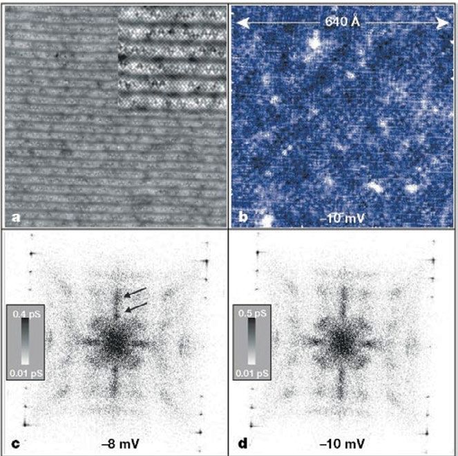
Scanning tunnelling microscopy laboratory can reduce tip–sample shaking well below
STM has at its heart a very simple idea: a metal needle 1 pm, which limits the fluctuation of the detected tunnel
that is sharpened to a single atom is approached very current within several per cent.
close to a surface while a biased voltage between the tip It is seemingly an impossible task to move the STM
and the surface is applied. When the tip–sample distance tip by atomic-scale dimensions without adding noise,
reaches the atomic-scale range, some electrons will jump but this has been made possible with the use of piezo-
between the tip and the sample, known as the tunnel- electric materials such as lead zirconate or lead titanate
ling current. The tunnelling current is sensitive to the ceramics1. A typical piezoelectric material used in STM
tip–sample distance; it has exponential dependence on will change its size by about 1 nm when a voltage of 1 V
the tip–sample distance. For example, in a clean vacuum is applied across its sides1. Hence, stable high-voltage
tunnel junction, the tunnelling current decreases by a sources can hold the tip stable to better than 1 pm while
factor of ten when the tip–sample distance increases by allowing a maximum scan range around 1 μm. However,
0.1 nm (the typical tip–sample distance is in the range as for STM systems under ultra-high vacuum (UHV)
0.3–1 nm). This effect gives STM its atomic-scale lateral conditions, it is necessary to change samples without
spatial resolution as the majority of the tunnelling current opening the vacuum chamber. The tip must be moved at
stems from only the last atom of the tip apex3 (Fig. 1a). least 1 mm away from the sample before the sample can
The STM tip is usually attached to piezoelectric con- be extracted. Although piezoelectric materials are good
trol elements that allow the tip to be moved with atomic- at atomic-scale length changes, they cannot provide
scale precision (Fig. 2a,b). In almost all STM systems, the such large displacements; instead, this task is achieved
tip and the sample should be replaced with new ones by the coarse approach mechanism with a type of piezo
in a convenient manner without violently changing the motor, which is the kernel component of the STM scan-
STM configuration. Generally, STMs are very sensitive ner head (Fig. 2b). The action of such a motor can be
to noise, which includes electronic noise and vibra- easily visualized: the tip is held on a body — often made
tional noise from the laboratory environment. Here, we from a ceramic — which is mounted on piezoelectric
Biased voltage focus on controlling some of these noise sources, from materials. When the piezo materials move slowly,
The DC voltage applied to the
large to atomic scale. The scanner head of the micro- the ceramic body will follow. However, when the piezo
tunnelling junction, either on
the sample or on the tip. scope, or the STM body, has macroscopic dimensions materials move rapidly (>100 nm in 10 µs), the body will
typically in the range of a few centimetres. By contrast, hold still owing to its inertia. Each step gives a motion in
Eddy current the tip–sample distance is often smaller than 1 nm. the range of 100 nm. This process can then be repeated
Loops of electrical current Ideally, the tip–sample distance is kept stable at approx- many thousands of times to arrive at a macroscopic
induced within a conductor
by changing the magnetic field
imately 1 pm. As the tunnelling current is sensitive to motion. Such a stick–slip motion5,6 is reliable in provid-
through this conductor based the tip–sample distance (and, hence, to fluctuations in ing coarse motion in the range of a few millimetres, but
on Faraday’s law of induction. this distance), mechanical shaking causes noise in the is among the most difficult parts of STM design as it is
2 | Article citation ID: (2021) 1:36 www.nature.com/nrmp
0123456789();: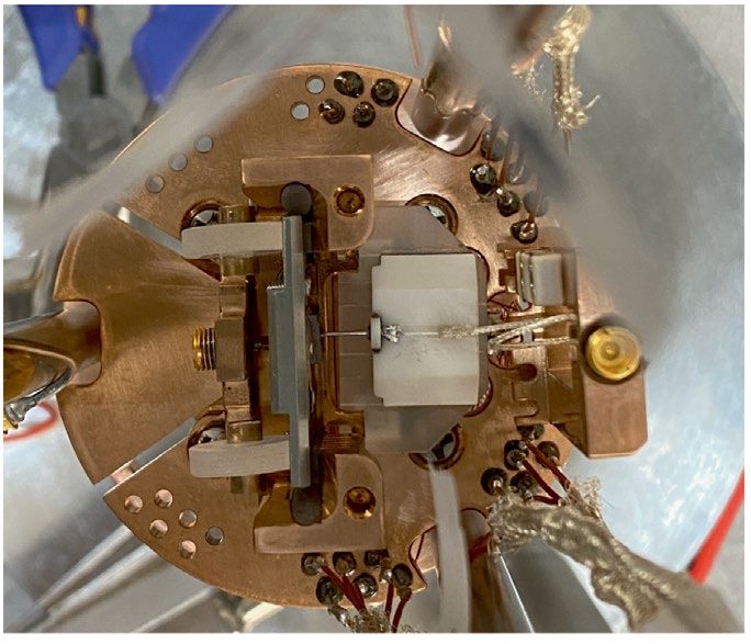
Primer
Mechanical resonance
challenging to provide a rigid enough movable motor Atomic force microscopy
frequency with mechanical resonance frequency larger than several As STM can only probe conductive surfaces relying on
The frequency at which a kilohertz. The well-known types of motor for the coarse the tunnelling current, AFM was conceived to extend
mechanical system vibrates approach include the louse type7, beetle type5, Pan type6 atomic resolution to non-conducting surfaces2. The
with greater amplitude than
it does at other frequencies,
and various single-tube types. advantage of AFM is that it can be employed in a vacuum,
generally determined by the There is no way to sharpen the tip to a single atom, an ambient atmosphere and a liquid, and from high to
stiffness and mass of this and so in situ protocols have been developed for this ultra-low temperatures. AFM shares many basic features
mechanical system. task. Most often, we start with either a cut platinum/ and key components with STM, such as the vibrational
iridium wire or with an etched tungsten wire8. A cut wire isolation, scanning process, coarse-approaching mech-
Quantum corrals
The barriers constructed by
has the advantage of fewer oxide films on its surface, anism and tip treatments. However, as AFM detects
individually positioning the iron whereas an etched tip has a much better macroscopic local force instead of the tunnelling current, there are
adatom through the scanning shape. The platinum/iridium tip can be produced by some differences in the signal acquisition and the feed-
tunnelling microscopy tip. mechanical cutting or electrochemical etching, whereas back loop (Fig. 1b). In AFM, a tip is mounted at the end
Local force
the tungsten tip can only be made by etching owing to of a flexible cantilever, which deflects linearly with the
The local interaction between tungsten’s brittleness. For most STM measurements, the force applied. Contact mode AFM measures tiny deflec-
the atoms on the tip apex overall shape of the tip does not matter as the tunnel- tions of the scanning cantilever and uses a force-feedback
and the surface within a ling only occurs from the atom or cluster of atoms at the circuit to move the sample or tip held by a piezoelec-
volume of several cubic
very end of the tip. However, for some applications — tric element in the z direction (maintaining a constant
nanometres.
most notably optical experiments — the macroscopic tip–sample distance) to keep the deflection, and thus the
Dynamical AFM shape can have a pronounced effect on the plasmonic applied force, constant. Plotting the z-direction position
A type of atomic force enhancement of Raman scattering and fluorescence9. (height) of the scanned surface pixel by pixel provides the
microscopy (AFM) where Lower temperatures are desirable for STM because sample topography. An important development for AFM
an oscillator (for example,
cantilever, tuning fork) works
of improved stability compared with room tempera- was the optical lever system18, which reflects a laser beam
at its resonance frequency, ture, as well as higher energy resolution owing to the on the backside of the cantilever to efficiently magnify the
detecting interactions between smaller thermal broadening of the electrons in both tiny cantilever deflections resulting from the interactions
the tip and the sample the tip and the sample. Eigler introduced a machine of the tip and the sample (Fig. 3a), thus largely enhanc-
through the changes of
with a stable design operating at about 5 K reaching ing the signal to noise ratio during data acquisition. An
frequency, amplitude and
energy compensation of this
a tip–sample distance noise below 1 pm, which was important development towards enabling biological AFM
oscillator. used to build quantum corrals10 and move individual was the invention of a liquid cell in which the cantilever
atoms11,12. Eventually, lower operating temperatures — and the sample are immersed in physiological solution19.
down to 10 mK (ref. 13 ) — were achieved; such Dynamical AFM uses oscillating cantilevers20. Concomi
ultra-low-temperature STM is also functional under tant amplitude modulation modes (for example, ‘inter-
high magnetic fields up to 30 T (ref.14). On the other mittent contact’, ‘tapping’ or ‘oscillating’ mode) use
extreme, STM has been used to image the growth of feedback controls to oscillate the cantilever at resonant
materials in situ at temperatures up to several hundred frequency and constant amplitude21 (Fig. 3b). Other oscil-
degrees Celsius15. STM has also been used to study cata- lating modes apply frequency (frequency modulation) or
lytic processes under near-ambient pressures16. Whereas phase (phase modulation) for feedback control (Fig. 3b).
operation of STM in air is often complicated owing to Such dynamic modes control the tip–sample interaction
the presence of water films on the surfaces of samples, more gently compared with static AFM modes so that
STM can work in a more stable manner at a solid–liquid interaction forces are minimized.
interface, where both the potential stability and the Frequency modulation AFM (FM-AFM) is used
chemical composition inside the aqueous environments for UHV and low-temperature physics22, as well as for
are well controlled17. biological applications23. FM-AFM is usually more
a b
Sharp metal tip Cantilever
I
V
e– Force
Sample
Fig. 1 | Basic set-up for scanning probe microscopy. Scanning tunnelling microscopy (STM) and atomic force microscopy
(AFM) both use a tip to scan the sample. Both techniques use different feedback signals to maintain constant tip–sample
interaction, but their basic principle of operation and image acquisition mechanisms are similar. a | STM collects the
tunnelling current between the tip apex and the sample when a bias voltage is applied. b | AFM detects local forces and
corresponding mechanical parameters through a spring-like cantilever.
NATURE REvIEWS | METHoDS PRimERS | Article citation ID: (2021) 1:36 3
0123456789();:
Primer
a Phase f2 – f1 f2 + f1
V0(f2,t) shifter ~
φ V
Vibration Constant current
isolation z V0(f2,t,φ) f
V(f1,t)
Constant height STS DC output
Coarse Multiplier Low-pass filter
motor Time
3D High voltage PID
scanner Preamplifier output
Bias
x y z
Tunnelling
Raster-scan Summator
current
Magnet
Controller
Damping Data
Analogue input
Modulator
b c 10–5
10–6
1/3 octave spectral density
RMS velocity (m s–1)
Tip Coarse
motor 10–7
Sample
10–8
10–9
10–10
1 10 100
Frequency (Hz)
IBM Almaden QNS floor
IBM ETH Zurich QNS block
MPI Stuttgart
Fig. 2 | Scanning tunnelling microscopy set-up. a | Scanning tunnelling microscopy (STM) set-up consisting of a coarse
motor, three-dimensional (3D) scanner, vibration isolation device, damping device, preamplifier and controller unit. The
frame shields the external electric noise. The proportional integral differential unit (PID) is used for controlling the tip–sample
distance in constant current operational mode. Inset: schematic showing lock-in for scanning tunnelling spectroscopy
(STS) measurements. The basic electric circuit demonstrates both the process of modulations and its corresponding
demodulations, where V is the modulated signal and V0 is the reference. b | Photograph of STM scan head with tip, sample
on sample holder and slip–stick walker, all mounted on a metal base plate. c | Vibration levels in various STM laboratories
from around the world between 1 and 200 Hz. y axis represents the velocity scaled in a fashion typical for architectural
comparisons. The lowest vibration levels are dependent on floating concrete blocks (IBM ETH Zurich, MPI Stuttgart,
QNS block), high-quality basement levels of laboratory buildings (QNS floor) and regular basement-level laboratory
floors (IBM Almaden). RMS, root mean square. Part c reprinted with permission from ref.4, Royal Society of Chemistry.
precise than amplitude modulation AFM, as the time It is more challenging to obtain high-resolution images
and frequency can be measured with higher accuracy in AFM systems, as forces have multiple long-range and
than amplitude changes. However, force detection by short-range components and the force–distance rela-
amplitude modulation AFM is simpler and faster, and tion between tip and sample can be more complicated
Temporal resolution
the amplitude changes with the tip–sample distance in than the current–distance relation in STM26,27. Presently,
The duration of time for
acquisition or capture of a a nearly monotonic manner. Time-lapse AFM imaging subatomic details such as orbitals or chemical bonds can
single event in measurements. can monitor cellular machines at work at the nanoscale be observed by probing short-range forces with chem-
level24. When using a small cantilever with a high res- ically functionalized tips in high vacuum. Meanwhile,
Functionalized tips onant frequency, time-lapse AFM can work at much researchers developed a plethora of new AFM-based
Modified tips with a single
molecule or specific clusters in
faster speeds, which allows observation of machinery approaches to probe chemical, magnetic and friction
order to make the tip adapted at a temporal resolution of ~100 ms (ref.25); this set-up is forces, and to introduce different spectroscopies such as
for specific applications. known as high-speed AFM. force spectroscopy with sub-piconewton sensitivity28,29
4 | Article citation ID: (2021) 1:36 www.nature.com/nrmp
0123456789();: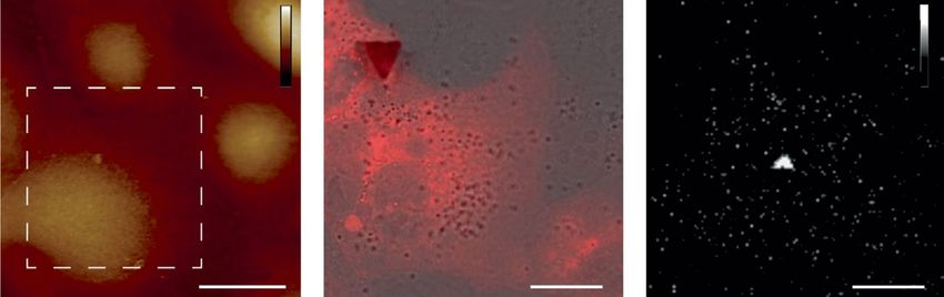
Primer

Quality factor
                                or single-molecule and single-cell force spectroscopy in          corresponding image will be measured at constant cur-
The dimensionless factor        biology30–32. Now, we approach the time at which AFM              rent in STM or constant force in AFM. On the other
describing the dissipation      imaging simultaneously quantifies and structurally maps           hand, when the feedback is not used, the tip height is
and damping of the mechanical   the various physical, chemical and biological properties          kept constant, resulting in the constant-height imag-
oscillator during a single
oscillating cycle.
                                of non-living and living objects24,33,34 (Fig. 3c).               ing mode. Under the constant-current/force mode,
                                    Progress in instrumentation has been key to recent            the tip–sample distance is determined by the preset
Thermal drift                   AFM developments. After the quartz tuning fork was                current/force and typically higher resolution is obtained
The steady and monotonic        first used as the force sensors for non-contact AFM35,            at smaller tip–sample distance, simultaneously with
changes of the specific
                                one example of prominent progress is the development              higher risk of tip damage. By contrast, constant-height
location or parameter with
time resulting from the
                                of the qPlus sensor, with one prong fixed to enhance              imaging only works for flat surfaces, and the results are
changed temperature.            the quality factor up to ~100,000 at small amplitude              more straightforward to interpret owing to the absence
                                (
Primer
Young’s modulus
(d2I/dV2), such as inelastic electron tunnelling spectros The SPM tip is not only a perfect probe for surface
A mechanical property that copy (IETS) (Fig. 4A). To obtain dI/dV and d2I/dV2 spec- characterization but also acts as a nanoscale hand
quantifies the relationship tra, a small voltage modulation is added to the bias, and for manipulating single atoms or molecules11,41,42. Precise
between tensile stress and the first-order and second-order components of I–V manipulation is usually achieved through voltage pulses
axial strain, which reflects
the tensile stiffness of a
curves are extracted by lock-in amplifiers (Fig. 2a). In or forces when the tip is positioned directly above the
solid material. AFM-based force spectroscopy, the tip is approached target sites. During such a process, the injected electrons
and withdrawn from a sample surface while record- can excite the vibrational modes of atoms or molecules
ing a force–distance curve (Fig. 4B). The force–distance and lead to diffusion, desorption and selective bond
curves allow analysis of repulsive and adhesive interac- breaking or formation42–44. For vertical manipulation,
tions between the tip and the sample, as well as sample an adsorbed molecule is picked up by an STM tip by
deformation and elasticity40 (Box 1). AFM can combine injecting electrons into the surface, transferred above a
imaging with force spectroscopy to simultaneously target site and then released from the tip by applying
map mechanical, chemical and biological properties. a reversed bias voltage, leading to the formation of a new
Therefore, the AFM record for each pixel of the result- complex42 (Fig. 4C). For the lateral manipulation, the tip
ing AFM topography represents a force–distance curve, is brought close to the atom or molecule on the sur-
from which multiple parameters such as Young’s modulus face, such that the tip–sample interaction force is large
and energy dissipation, pressures and tension can be enough to pull or push the atom or molecule moving
extracted (Fig. 3c). over the diffusion barrier41,45 (Fig. 4D).
A B Ca [110]
F
[001]
Tip
Elastic tunnelling e–
O
hω Fe
eV C
Inelastic tunnelling Ag
z Cb
Tip Sample
I
Elastic
Inelastic Pauli repulsion Attractive Cc
–E0 E0 V Short-range chemical force Repulsive
Long-range electrostatic/ Total interaction
van der Waals interaction
dI/dV
e–
D
–E0 E0 V
Tip path
Cd
d2I/dV2 Force
Substrate
–E0
E0 V
Fig. 4 | Schematics of scanning probe spectroscopy and manipulations. the attractive force and repulsive force versus tip distance, respectively.
A | Schematic revealing inelastic tunnelling (red) and elastic tunnelling C | Schematic showing formation of a single bond through scanning
(blue). Vibrational excitation indicated by wavy lines, which leads to an tunnelling microscopy. A single molecule can be detached (part a),
increase in conductance. Graphs show an I–V curve and corresponding translated (part b) and attached onto another adatom through precise
dI/dV and d2I/dV2 spectra where extra tunnelling conductance caused manipulation of the scanning tunnelling microscopy (STM) tip (parts c,d).
by inelastic tunnelling appears at ±E0. Dashed lines reflect the elastic and D | Schematic showing the process of laterally pulling an adatom
inelastic tunnelling channels, whereas solid lines show the actual data. through the STM tip. Jump height (green arrow), lateral distance between
B | Schematic showing typical force–distance curves. Both short-range the tip apex and the manipulated adatom (red arrow), and tip height
(green region, Pauli repulsion; blue region, short-range chemical force) (blue arrow) during manipulation are indicated. Part C adapted with
and long-range (orange region, long-range electrostatic or van der Waals permission from ref. 42, AAAS. Part D adapted with permission from
interaction) components are indicated. Black and grey curves represent ref.41, APS.
6 | Article citation ID: (2021) 1:36 www.nature.com/nrmp
0123456789();: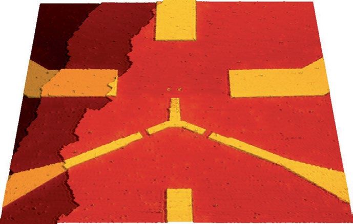
Primer
Tip preparation and functionalization Box 1 | Single-molecule force spectroscopy
Atomically sharp tips are the key to achieving high res-
olution in SPM. They are usually produced by mechan- The uniqueness of directly probing physical interactions
ical cutting or milling, electrochemical etching or more between the atomic force microscopy (AFM) tip and
complicated nanofabrication such as focused ion beam the biological sample has been exploited to develop single-
molecule force spectroscopy. This technique measures
systems46. However, the tip apex obtained by those meth-
the bonds of single receptor–ligand pairs. In the early
ods is not sharp enough for atomically resolved imaging. days of single-molecule force spectroscopy, the AFM
To obtain an ideal tip terminated with a single atom or a tip (or a bead glued to the tip) was functionalized with
small cluster of atoms, the tip needs to be treated (which ligands and the surface of the support, such as a bead
includes both sharpening and functionalization) during on top of the substrate, with receptors30,288. If the tip
scanning by poking the tip into the surface and grasping and sample are brought into sufficient proximity, the
a small cluster of atoms. In STM experiments, the appli- ligand and receptor can bind. The AFM tip is then
cation of high voltages up to 10 V can be used for tip withdrawn, and the force required to separate the
treatment, at a tip–sample distance of ~1 nm to induce specific bond is measured. This unbinding force describes
field emission47. The atoms at the very end of the tip the mechanical strength of the receptor–ligand bond.
Typically, such experiments are repeated several
determine the spatial resolution of SPM, not the overall
thousand times to characterize a sufficient number
radius of curvature at the apex. In order to obtain high of successful binding and unbinding events. The use of
chemical resolution besides topography, one can also short cantilevers in high-speed AFM set-ups extends
evaporate noble metal films such as gold and silver onto the accessible dynamic range in force spectroscopy
the conventional silicon AFM tip; this type of tip has experiments to measure molecular dynamics
been extensively used for nanoscale chemical analysis simulations319, whereas low-noise AFMs reach force
under ambient conditions48,49. sensitivity comparable with that of optical tweezers320.
For SPM experiments performed in UHV and low-
temperature conditions, the most controllable and pre- chemical and biological interactions40. One approach to
cise way to get a well-defined sharp tip is functionalizing study these interactions is to functionalize the AFM tip.
the tip apex by picking up a single atom or molecule
on the surface50,51. Under such conditions, SPM with Variations of SPM
a CO-functionalized tip can image molecular orbitals52, By integrating microsensors on the tip or coupling the
owing to the p-wave orbitals of the CO molecule. The electromagnetic waves with different wavelengths into
CO tip also allows access to the short-range Pauli the tip–sample junctions, a large family of SPM methods
repulsions, reflecting the variations of electron density have been developed since the invention of STM and
in individual chemical bonds53. As the CO tip has a AFM. In this section, we introduce some representative
quadrupole-like charge distribution, it is also sensitive variations of SPM, which can map out various physical
to the high-order electrostatic force54. One drawback quantities besides current and force, such as magnetic/
of the CO tip is the lateral relaxation of the CO mole- electric field, photons, strain, temperature, and dielectric
cule at the tip apex, which leads to distortion or even and physiological responses. The sensing mechanism,
artefacts in the SPM images. Functionalizing the tip at advantages and applications of those SPM variations are
the atomic level, for example replacing the C–O group briefly discussed in the following sections.
with oxygen55 and chlorine56, yields a more rigid tip with
smaller relaxation of the tip apex. However, the reso Time-resolved STM. Despite achieving high spatial reso-
lution of those tips is usually poorer than for the CO tip, lution in real space, one of the most interesting questions
as strong relaxation of the CO molecule is also crucial about SPM is the speed at which such a device could
to obtain sharply resolved structural resolution when capture a signal in real time. High-speed image acqui-
the tip–sample distance is within the region of Pauli sition could be achieved by video-rate STM15,61, which
repulsion57. typically scans a frame within a millisecond timescale.
For biological AFM imaging applications, tips Recently, with the pulsed voltages, fast spin dynamics
are typically made of silicon or silicon nitride, which such as spin relaxation was investigated by electrical
upon exposure to air and immersion into physiologi- pump-probe STM at the level of a single atom62. As the
cal buffer will feature an oxide layer at their surface58. bandwidth of the preamplifier and other electronics of
To achieve sharper tips with higher aspect ratio, elec- SPM is limited to megahertz, ultra-fast dynamics within
tron beam deposition can be used, resulting in the picoseconds and femtoseconds should be captured by
growth of an amorphous carbon-based apex, which is incorporating pump-probe techniques into STM, lead-
subsequently rendered hydrophilic using plasma clean- ing to femtosecond laser STM63,64 and terahertz STM65,66.
ing59. Carbon nanotubes have been grafted as a quasi Examples of various time-resolved STM techniques can
one-dimensional (1D) object at the end of AFM tips to be found in Table 1.
create a super-sharp, very high aspect ratio apex, but
despite efforts these tips have so far had no significant Magnetic field-sensitive SPM. Magnetic field or spin-
impact in the AFM field, likely because of nanotube sensitive SPM is very useful for characterizing local mag-
CO-functionalized tip buckling60. Overall for biological imaging applications netic structures and spin states in real space (Table 2).
Modification of the tip with a
single CO molecule in order to
in liquid, the tip–sample interaction forces range from The simplest method for detecting the local magnetic
enhance the spatial resolution short range (≈1–10 nm) to long range (>10 nm) and field is by replacing the conventional non-magnetic
of scanning probe microscopy. can be composed of a repertoire of different physical, probe with a magnetic probe, which is extensively used
NATURE REvIEWS | METHoDS PRimERS | Article citation ID: (2021) 1:36 7
0123456789();: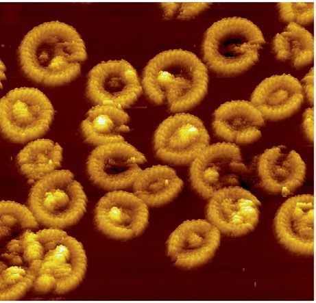
Primer
Table 1 | Time-resolved scanning probe microscopy techniques
Name Detected signal Utility Resolution Disadvantages and Refs
limitations
Video-rate Tunnelling current Fast dynamics Atomic resolution Spatial resolution is poor 15,61
scanning tunnelling during chemical and millisecond owing to short integration
microscopy reactions, surface temporal time; temporal resolution
reconstruction resolution is limited by the resonance
and material frequency of the scanner
growth at elevated and the bandwidth of the
temperatures electronics
Electrical pump- Tunnelling current Fast electron spin Atomic resolution Time resolution is limited 62
probe scanning dynamics and nanosecond by the bandwidth of
tunnelling temporal advanced electronics such
microscopy resolution as the preamplifier and
pulse generators
Femtosecond laser Photo-induced Ultra-fast charge, Atomic resolution Laser-induced thermal 63,64
scanning tunnelling tunnelling current spin and phonon and femtosecond expansion of the tip can
microscopy dynamics at the temporal lead to artificial signals
atomic scale resolution
Terahertz scanning Photo-induced Ultra-fast charge, Atomic resolution Introduction of 65,66
tunnelling tunnelling current spin and phonon and femtosecond terahertz light into
microscopy dynamics at the temporal the ultra-high vacuum
atomic scale resolution and low-temperature
scanning tunnelling
microscopy system is
complicated; the temporal
resolution is limited by the
wavelength and width of
the terahertz pulse
in magnetic force microscopy67,68, magnetic exchange for use in aqueous environments. The self-assembly and
force microscopy 69 and spin-polarized STM 70,71 . reactivity of supramolecular systems inside non-ionic
Another avenue is grafting a micro-magnetic sensor organic liquids has been investigated by liquid-phase
such as a superconducting quantum interference device STM85–87. Meanwhile, working at the solid–electrolyte
(SQUID) or Hall probe on the tip, constructing scan- interfaces, electrochemical STM (EC-STM) is developed
ning SQUID microscopy72,73 and scanning Hall probe with four electrodes including the tip, working elec-
microscopy74. In addition, by incorporating microwaves trode, counter electrode and reference electrode, which
into SPM to excite magnetic resonance, the magnetic are controlled by a bipotentiostat17,88. As EC-STM only
sensitivity of SPM can be enhanced up to single electron works on conductive surfaces, liquid-phase non-contact
or nuclear spin, such as electron spin resonance (ESR) AFM was developed for imaging the local structures on
STM75–77, magnetic resonant force microscopy78 and insulator–liquid interfaces89,90. In order to characterize
nitrogen vacancy-based SPM79. complex biological systems such as living cells in phys-
iological buffers with high spatial resolution, scanning
Electric field-sensitive SPM. To map out the surface ion conductance microscopy should be chosen91. In this
potential or charge with high resolution, typically a system, the ion current flow from the tip to the refer-
conductive SPM tip biased with variable voltage is ence electrodes in the solution is monitored and used for
used (Table 3). One form of electric field-sensitive SPM feedback to control the tip–surface distance. Compared
is scanning capacitance microscopy80, where the local with EC-STM and liquid-phase AFM mentioned above,
capacitive coupling between the tip and the sample is scanning ion conductance microscopy provides the
detected for deriving the local dielectric and electrical unique possibility of locally probing the ion transport
properties. Another option for sensing local potential of biological systems by monitoring the ion current92.
is the integration of a microelectric sensor such as a Similarly, AFM can scan a hollow microcantilever to
single-electron transistor onto the tip81. For single charge perform scanning ion conductance microscopy mea
Hall probe
A micron-sized device for
detection, the tip should be brought as close as possible surements, which is also called fluid force microscopy,
detecting the external to the sample, which requires a sharp metal tip instead to patch clamp or to manipulate living cells93,94. Examples
magnetic field through of a microelectric sensor, such as in Kelvin probe force of liquid-phase SPM can be found in Table 4.
the Hall effect. microscopy82. Piezoresponse force microscopy (PFM)
is another important electric-field sensitive SPM83,84, Electrical transport-compatible SPM. In order to make
Bipotentiostat
An electronic system in which a modulated pressure is applied locally on SPM suitable for investigating local electron transport
capable of controlling two the sample by the tip and its piezoelectric response is properties both on the surface and the interface of sam-
potentiostats, which include monitored during scanning. ples such as 2D material-based novel electronic devices,
two working electrodes, one various electrodes should be fabricated on the surface
shared reference electrode
and one shared counter
Liquid-phase SPM. Although surface characterization in addition to the bias electrode, acting as source, drain
electrode for electrochemical with atomic resolution is ever-present in UHV and and electric gates. Immediately after the appearance of
measurements. low-temperature experiments, it remains challenging STM, scanning tunnelling potentiometry was invented
8 | Article citation ID: (2021) 1:36 www.nature.com/nrmp
0123456789();: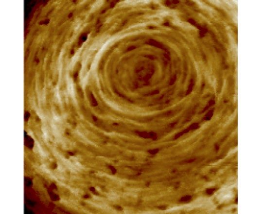
Primer

                             Table 2 | Magnetic field-sensitive scanning probe microscopy techniques
                             Name                  Detected signal         Utility                Resolution         Disadvantages and         Refs
                                                                                                  and                limitations
                                                                                                  sensitivity
                             Spin-polarized        Spin-polarized          Nanoscale              Atomic             High-energy resolution     70,71

                             scanning tunnelling   tunnelling current      spin texture           resolution         only works on
                             microscopy                                    or long-range          with sensitivity   conductive samples
                                                                           spin ordering of       of single          under low temperature
                                                                           magnetic materials     electron spin      and ultra-high vacuum
                             Electron spin         Spin-polarized          Spin identification,   Atomic             The spin-polarized        75–77

                             resonance             tunnelling current      electron spin          resolution         tip is not only a probe
                             scanning tunnelling                           resonance spectra/     with sensitivity   but has an effect on
                             microscopy                                    imaging and            of single          the coherence of the
                                                                           quantum sensing        electron spin      target spin
                             Magnetic force        Dipolar magnetic        Magnetic structures    Spatial            The magnetic tip           67,68

                             microscopy            interaction             of sample surfaces     resolution of      will disturb the
                                                                                                  several tens       magnetic state of
                                                                                                  of nanometres      the sample, and vice
                                                                                                                     versa, complicating
                                                                                                                     quantitative
                                                                                                                     interpretation
                                                                                                                     of the magnetic
                                                                                                                     force microscopy
                                                                                                                     measurement; atomic
                                                                                                                     resolution cannot be
                                                                                                                     achieved owing to the
                                                                                                                     long-range magnetic
                                                                                                                     forces between tip
                                                                                                                     and sample
                             Scanning              Magnetic flux and       Scanning               Spatial            Only works under low       72,73

                             superconducting       superconducting         magnetometry and       resolution of      temperature; spatial
                             quantum               current                 thermometry at low     several tens       resolution is limited
                             interference device                           temperature            of nanometres      by the size of the
                             microscopy                                                           and magnetic       superconducting loop
                                                                                                  sensitivity
                                                                                                  up to single
                                                                                                  electron spin
                             Nitrogen vacancy      Fluorescence of the     Scanning               Spatial            The quantum sensor           79

                             centre scanning       nitrogen vacancy        magnetometry of        resolution of      is buried underneath
                             probe microscopy      centre                  nanoscale magnetic     ~10 nm and         the diamond surface,
                                                                           textures at various    magnetic           which makes atomic
                                                                           temperatures;          sensitivity        resolution challenging;
                                                                           compatible             up to single       the shallower nitrogen
                                                                           with an ambient        nuclear spin       vacancy has poorer
                                                                           environment and                           quantum coherence,
                                                                           biological systems                        which decreases the
                                                                                                                     signal to noise ratio
                                                                                                                     and sensitivity
                             Magnetic resonance    Magnetic dipolar        Nanoscale electron     Resolution         Only works under             78

                             force microscopy      interaction             and nuclear
Primer

                                   Table 3 | Electric field-sensitive scanning probe microscopy techniques
                                   Name               Detected signal        Utility                    Resolution and       Disadvantages and          Refs
                                                                                                        sensitivity          limitations
                                   Scanning           Tunnelling current     Local electric field and   Spatial resolution   Only works under low           81

                                   single-electron                           potential caused by        of several tens of   temperature; spatial
                                   transistor                                the local charges,         nanometres and       resolution is limited by
                                   microscopy                                especially the local       electric field       the size of the device
                                                                             electronic states of       sensitivity up to
                                                                             strongly correlated        2 μV Hz–1/2
                                                                             materials
                                   Scanning           Capacitance            Dielectric and             Spatial resolution   Spatial resolution             80

                                   capacitance                               electrical properties      of several           is limited by the
                                   microscopy                                of semiconductors          nanometres with      long-range capacitance
                                                                             and buried                 capacitance          coupling
                                                                             two-dimensional            sensitivity of
                                                                             electron gas               attofarad
                                   Kelvin probe     Contact potential        Local work function        Nanoscale spatial    Unsuitable for                 82

                                   force microscopy difference               and electric dipole        resolution with      characterization of
                                                                             distribution of various    sensitivity up to    voltage-sensitive
                                                                             samples                    a single charge      samples; spatial
                                                                                                                             resolution is limited
                                                                                                                             by the long-range
                                                                                                                             electrostatic force
                                   Piezoresponse    Piezoelectric            Ferroelectric ordering, Spatial resolution Tip wear can modify the           83,84

                                   force microscopy response of the          piezo coefficient and   with several       tip–surface interaction,
                                                    sample                   energy dissipation      nanometres         affecting imaging
                                                                                                                        contrast; the acquired
                                                                                                                        force signals may not
                                                                                                                        always arise from
                                                                                                                        piezo/ferro electricity
                                                                                                                        phenomena

                                  for investigating the local distribution of potential and      tip-enhanced Raman spectroscopy (TERS)9,48. Recently,
                                  inhomogeneous conductivity of metals and semiconduc-           TERS has demonstrated its ability in identifying and
                                  tors95. Without the need for detecting the tunnelling cur-     resolving chemical structures of single molecules with
                                  rent, scanning gate microscopy uses a conductive tip as the    sub-nanometre resolution9. Benefiting from the local
                                  movable electric gate and is capable of revealing the local    plasmon confined within the tunnelling junction, scan-
                                  gating effects on the transport currents from the source       ning tunnelling microscope-induced luminescence was
                                  and drain96,97. As the electrodes for transport measure-       also developed and applied for detecting the optical
                                  ments are usually fixed by nanofabrication, much more          emission from the electronic and vibrational transition
                                  precise and flexible positioning of such electrodes was        at the single-molecule level103. Apart from working within
                                  realized by multi-probe STM98,99 (Table 5).                    the range of visible light, it is also attractive for investi-
                                                                                                 gating the dielectric response of materials in the mega-
                                  Near-field SPM. To optically probe the structural, dielec-     hertz to gigahertz regime, such as microwave impedance
                                  tric and chemical properties with visible sub-wavelength       microscopy, where a sharp metallic tip extended from
                                  resolution, scanning near-field optical microscopy             a high-frequency resonator was used as the antenna to
                                  (SNOM) was developed and has been widely used in the           emit and collect microwave photons104,105. In contrast
                                  past decades100 (Table 6). SNOM makes use of the eva-          to conventional near-field SPM, photo-induced force
                                  nescent components of the light highly confined near the       microscopy106 directly detects the near-field signal
                                  surface, thus overcoming the diffraction limit of far-field    based on photo-induced dipolar forces, which efficiently
                                  optics. Generally, a sharpened optical fibre with a metal      suppress the overwhelming background signals.
                                  shield and a nanoscale aperture is used as the light
                                  source or detector for scanning. However, the spatial          Results
                                  resolution is limited by the aperture size of the optical      SPM images are always acquired as a 2D matrix, whereas
                                  fibre, with a typical value of 30–50 nm. By contrast, aper-    spectroscopic curves are saved in the form of arrays.
                                  tureless SNOM such as scattering-type SNOM101 uses a           The main steps for data analysis include image inspec-
                                  metallic AFM tip as the near-field scatterer and works         tion, noise analysis, filtering and image reconstruction.
Scanning gate microscopy          in a dynamical mode for suppressing the background             For the curves of SPM spectra and the line profiles of
A kind of scanning probe          far-field signals, which improves the spatial resolution       topographic images, a fitting procedure is usually nec-
microscopy capable of             up to 1 nm (ref.102). Furthermore, making use of a sharp       essary for interpretation of the underlying quantities
probing electrical transport      noble tip and highly confined surface plasmon101, the          and parameters. In this section, we showcase several
at the nanoscale, where a
conductive tip is used as the
                                  efficiency of Raman scattering in the tip–sample gap           representative examples to discuss how to analyse SPM
local gate capacitively coupled   is enhanced several orders of magnitude as compared            images and spectra. The popular software for processing
to the sample.                    with conventional far-field Raman experiments, such as         the SPM data are briefly introduced.

10 | Article citation ID:     (2021) 1:36                                                                                              www.nature.com/nrmp

                                                                    0123456789();:
Primer
Representative results biomolecules, the interaction force is detected and used
SPM imaging provides pseudo-3D data. As a surface to describe the deformations of the sample33 (Fig. 5c).
probing technique, it does not deliver information about On the other hand, upon withdrawing the tip, the force–
the inside volume of the object under investigation but distance curve can be used to infer multi-mechanical
provides an x–y grid of data points to each of which a sin- parameters such as adhesion, Young’s modulus, plas-
gle z height is associated. SPM data are thus most often tic deformation and energy dissipation of the sample
represented as an x–y 2D image, where a false-colour through fittings.
scale represents the z height107 (Fig. 5a). Sometimes, SPM STS is suitable for investigating the local density
data are represented as a 3D surface shown in perspec- of states of a sample. In Fig. 5d, a typical dI/dV curve
tive (Fig. 5b) that is visually attractive but scientifically acquired on a single pentacene molecule shows prom-
less precise because at least one of the in-plane axes is inent peaks at both the positive and negative biases,
skewed, the z height sometimes increased and some which are attributed to the highest and lowest molecular
structural features obstructed by the perspective view. orbitals (HOMO and LUMO, respectively)37. By fixing
In the SPM field, unfortunately, no stringent standards the bias at the LUMO or HOMO and spatially mapping
have been established regarding the representation of out the dI/dV intensity, the frontier orbitals of the sin-
SPM data in publications, and sometimes filters are gle pentacene molecule can be directly visualized in real
used to display images. Specifically, the application of space37 (Fig. 5f). Whereas the STM mode is only sensitive
short-range median filters in the y dimension, which to the electronic states near the Fermi level, non-contact
cancel lines from the fast scan axis (x dimension) of the AFM working under the frequency modulation mode
image acquisition, is common. is able to probe the total electron density of the sample
Force–distance curves are acquired by recording by entering into the region of short-range Pauli repul-
the deflection signal of the AFM cantilever while con- sion108. In Fig. 5g, a CO-functionalized tip clearly resolves
trolling the tip–sample distance. For example, when the chemical skeleton of the single pentacene molecule,
the tip approaches the surface and interacts with the where the short-range Pauli repulsion dominates the
Table 4 | Liquid-phase scanning probe microscopy techniques
Name Detected signal Utility Resolution Disadvantages and Refs
limitations
Scanning ion Ion current Non-invasive imaging Spatial resolution Spatial resolution is 91,92
conductance of the tomography with several tens limited by the size of
microscopy and investigation of nanometres the microchannel
of the physiological
properties of complex
biological systems
such as living cells
in solutions
Fluidic force Deflection of Single-cell Sub-micrometre Spatial resolution is 93,94
microscope the cantilever manipulation and limited by the size of
controlled delivery the microchannel
of bioactive agents
Liquid-phase Tunnelling current Investigation of Atomic resolution Tip condition is not 85–87
scanning supramolecular well controllable
tunnelling systems and their compared with
microscope self-assembly, scanning tunnelling
dynamics and reactivity microscopy in an
ultra-high vacuum;
only a conductive
surface could be
investigated
Electrochemical Tunnelling current In situ detection Atomic resolution Tip condition is not 17,88
scanning of various easily controllable
tunnelling electrochemical for electrochemical
microscopy processes, such reactions; Faraday
as formation of an currents interfere with
electrochemical the tunnelling current
double layer, metal
corrosion and
electrodeposition
Liquid-phase Frequency shift In situ detection of Atomic resolution Three-dimensional 89,90
non-contact the structure of the force mapping for
atomic force hydration layer and structural analyses on
microscopy electrochemical solid–liquid interfaces
double layer on a solid– is time consuming; only
liquid interface with local liquid density can
atomic resolution be probed
NATURE REvIEWS | METHoDS PRimERS | Article citation ID: (2021) 1:36 11
0123456789();:Primer
Table 5 | Transport-compatible scanning probe microscopy techniques
Name Detected signal Utility Resolution Disadvantages and Refs
limitations
Scanning Tunnelling current Imaging of the Atomic resolution Interpretation of the 95
tunnelling spatial distribution in principle signal is difficult because
potentiometry of electrostatic distinguishing tomography
potential from potentiometry is
challenging
Scanning gate Conductance Spatial mapping of Spatial resolution As the capacitive coupling 96,97
microscopy between source electron flows in of several tens of between tip and sample
and drain two-dimensional nanometres is long range, the spatial
electrodes materials and resolution is largely limited
semiconducting by the sharpness of the tip
materials apex and the tip–sample
distance
Four-probe Tunnelling current Local and in situ Atomic resolution Closest distance (10–20 nm) 98,99
scanning investigation of in principle between the probes is limited
tunnelling in-plane electronic by the curvature radius of
microscopy transport properties the tip apex; performance is
generally poorer than that
of conventional scanning
tunnelling microscopy
owing to the complex
scanner design
tip–molecular interaction108. The sharp lines arise from Here, we take the application of AFM in biology as
the electron density build-up across the covalent bonds an example. When AFM is used for cellular imaging,
between the carbon atoms. either proprietary software is used for analysis or images
In some cases, inelastic electron tunnelling signals are exported in various file formats such as .tiff, .raw,
may be superimposed on the large background of elas- .png, .sxm and .gwy to be analysed by laboratory-written
tic tunnelling conductance during STS measurements. routines in the software packages mentioned above or in
For example, the dI/dV curve taken on the bilayer MATLAB112. Analysis of data from the above-described
NaCl(001) film grown on Au(111) demonstrates a broad hybrid imaging/nanomechanical mapping modes113 is
peak (grey), which corresponds to the interfacial elec- often done in proprietary application mode software;
tronic states109 (Fig. 5e). When the tip is positioned on the in this case, not only the data encoding but also the
water molecule adsorbed on the surface, distinct kinks acquisition process is system-dependent. When AFM
appear in addition to the interfacial electronic states is used for molecular imaging and analysis of protein
(red). Such kinks are more clearly resolved as dips and structures and conformations, AFM users often borrow
peaks in d2I/dV2 spectra, which are point-symmetrical methods from electron microscopy. The recent progress
with respect to the zero bias. The energy positions of in electron microscopy to solve protein structures114 is
those features reflect the energies of different vibrational directly associated with image analysis developments.
modes of the single water molecule. To this end, there is a plethora of such programs for
analysis of macromolecular structures, such as EMAN115,
Visualization and analysis software IMAGIC 116, SPIDER 117 and RELION118. Given that
The major problem of image visualization and image the contrast transfer function and the noise distribu-
analysis originates from the fact that, so far, no com- tion of AFM are very different from those of electron
mon SPM file format has been established. Each SPM microscopy, these programs must be adapted with care.
company has a specific proprietary file format and SEMPER and MRC are most powerful to analyse 2D
microscope-associated software for image data analysis. crystalline data58, and most other programs are adapted
Among others, Gwyddion110, WSxM111 and ImageJ are to analyse single particles119.
free and open source software. They are likely the most
powerful SPM data visualization and analysis platforms, Analysis of biological data
as they provide a large number of data processing func- When using AFM for the analysis of images of pro-
tions. These include standard statistical characterization, teins, one particle is used for a cross-correlation
data correction, filtering and grain marking functions. search of all other molecules in the image. Next, cross-
Gwyddion and WSxM are compatible with most stand- correlation-based lateral and rotational alignment of
ard file formats (such as .dat, .txt and .sxm) acquired the particles is performed. Particle selection based on
from commercial SPM programs such as Nanonis, cross-correlation values can be performed to calculate
Omicron and RHK. ImageJ has the advantage that it is an average of the most common particle structure120.
widely used by the optical fluorescence microscopy com- During the averaging process, a standard deviation
munity and, thus, features a large variety of functions map can be calculated that highlights the most flexi-
that can be adapted for SPM data, and its capabilities are ble parts in the molecule121. From the stack of particle
rapidly growing through contributions of analysis tools images that one has extracted using cross-correlation
from a large scientific community. searches, one can statistically assess any parameter of
12 | Article citation ID: (2021) 1:36 www.nature.com/nrmp
0123456789();:Primer
interest characterizing the molecule, such as the height representations accompanied with statistical data, as is
and volume distribution of the particles122, or molecular done in the electron microscopy field.
symmetry123. For example, the complete perforin 2 rings
shown in Fig. 5a can be distinguished from incomplete Applications
arcs using cross-correlation-based selection and later- SPM has found a multitude of applications in the natural
ally and rotationally aligned to calculate an ensemble sciences. In the following, we divide those applications
average (Fig. 5a, insets). For the analysis of filamentous into physics, chemistry, materials science and biology,
structures, such as DNA or filamentous proteins, auto- although they are often closely linked to each other and
mated particle detection based on the height above the have strong overlap.
background, followed by tracing of the filaments, allows
direct extraction of the physical properties of the fila- Examples from physics
ment, such as its persistence length124. Unfortunately, Surface science. The initial application for STM was in
structural analysis using automated programs is not the field of surface science, where atomic-scale arrange-
utilized enough in the AFM field, and it is still rather ment as well as the electronic properties of materials
common to place arrows on image panels to high- needed investigation. The key initial experimental
light features instead of calculating relevant molecular evidence for the power of STM in this regard was the
Table 6 | Near-field scanning probe microscopy
Name Detected signal Utility Resolution and Disadvantages and Refs
sensitivity limitations
Scanning near-field Emission of Local fluorescence Spatial resolution Spatial resolution 100
optical microscopy fluorescence or imaging of biological with tens of is largely limited
adsorption of molecules and nanometres by the size of the
excitation lights photoluminescent nanofibres used as
spectroscopy of probes; near-field
semiconductors signal is weak and
easily disturbed by
metallic coatings
Scattering-type Elastic scattering Local dielectric Spatial resolution Requires cantilevers 101,102
scanning near-field of lights response from optical up to 1 nm and to work under
optical microscopy light and plasmonic monolayer large amplitude to
structures sensitivity eliminate far-field
background,
making the method
insensitive to
short-range tip–
sample interactions
Tip-enhanced Raman scattering Analysis and Single-molecule High spatial 9,48
of lights identification of sensitivity and resolution relies on
Raman scattering
the local chemical sub-nanometre the electromagnetic
structure of spatial resolution coupling between
small molecules, the tip and a
biomolecules, plasmonic substrate,
living cells and thus limiting the
two-dimensional systems that can
materials be studied
Scanning tunnelling Photon emission Photon yield images Single-molecule High spatial 103
microscope-induced from sample and energy-resolved sensitivity and resolution relies on
luminescence spectroscopic images sub-nanometre the electromagnetic
spatial resolution coupling between
the tip and a
plasmonic substrate,
thus limiting the
systems that can
be studied
Microwave impedance Reflection or Local dielectric Spatial resolution Spatial resolution 104,105
microscopy transmission properties and of several tens of is limited by the
parameters of conductivities; nanometres long wavelength of
microwaves suitable for obtaining microwave photons
information from a
buried interface
Photo-induced force Photo-induced Detection of both Spatial resolution Quantitative 106
microscopy dipolar topography and of sub-10 nm interpretation of
interactions chemical signature on and monolayer the imaging contrast
organic and inorganic sensitivity is difficult; only
samples works with the
narrow band of
infrared lights
NATURE REvIEWS | METHoDS PRimERS | Article citation ID: (2021) 1:36 13
0123456789();:You can also read