Scanning Tunneling Microscopy
←
→
Page content transcription
If your browser does not render page correctly, please read the page content below
Scanning Tunneling Microscopy
                   Nanoscience and Nanotechnology
   Laboratory course "Nanosynthesis, Nanosafety and Nanoanalytics"
                                LAB2

                         Universität Siegen
                 updated by Jiaqi Cai, April 26, 2019

Cover picture: www.nanosurf.com

Experiment in room ENC B-0132
AG Experimentelle Nanophysik
Prof. Carsten Busse, ENC-B 009
Jiaqi Cai, ENC-B 026

                                  1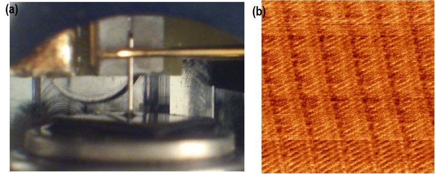
Contents
1 Introduction                                                                                              3
2 Surface Science                                                                                           4
  2.1   2D crystallography . . . . . . . . . . . . . . . . . . . . . . . .                                   4
  2.2   Graphite . . . . . . . . . . . . . . . . . . . . . . . . . . . . . .                                 5

3 STM Basics                                                                                                 6
  3.1   Quantum mechanical tunneling . . . . . . . . . . . . . . . . .                                       7
  3.2   Tunneling current . . . . . . . . . . . . . . . . . . . . . . . . .                                  9

4 Experimental Setup                                                                                        12
5 Experimental Instructions                                                                                 13
  5.1   Preparing and installing the STM      tip   .   .   .   .   .   .   .   .   .   .   .   .   .   .   13
  5.2   Prepare and mount the sample .        . .   .   .   .   .   .   .   .   .   .   .   .   .   .   .   15
  5.3   Approach . . . . . . . . . . . . .    . .   .   .   .   .   .   .   .   .   .   .   .   .   .   .   16
  5.4   Constant-current mode scan . . .      . .   .   .   .   .   .   .   .   .   .   .   .   .   .   .   17
  5.5   Arachidic acid on graphite . . . .    . .   .   .   .   .   .   .   .   .   .   .   .   .   .   .   18
  5.6   Data analysis . . . . . . . . . . .   . .   .   .   .   .   .   .   .   .   .   .   .   .   .   .   20

6 Report                                                                                                    21
  6.1   Exercise . . . . . . . . . . . . . . . . . . . . . . . . . . . . . .                                21
  6.2   Requirements . . . . . . . . . . . . . . . . . . . . . . . . . . .                                  21

                                       2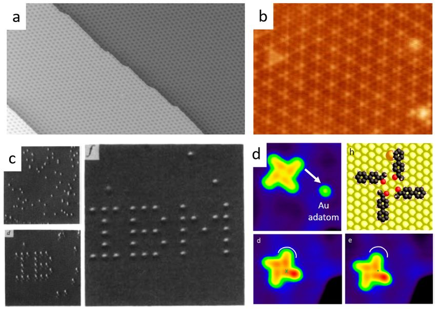
1 Introduction
In this lab course, you will learn about scanning tunneling microscopy (STM).
For the invention of the STM, Heinrich Rohrer and Gerd Binnig received
the Nobel prize for physics 1986 [1]. The STM operates by scanning a con-
ductive tip across a conductive surface in a small distance and can resolve
the topography with atomic resolution. It can also measure the electronic
properties, for example the local density of states, and manipulate individ-
ual atoms or molecules, which are adsorbed on the sample surface. Some
examples are shown in Figure 1.
Figure 1: a) Graphene on Ir(111), Voltage U =0.1V; Current I =30nA [2], b)
NbSe2 (showing atoms and a charge density wave (CDW)) [3], c) manipu-
lation of Xe atoms on Ni(110). U = 0.01V; I = 1nA [4], d) loading and
transport of a single atom with a supra-molecular transporter. U = 0.1V;
I = 0.1nA [5].
Besides the usage of the STM, you will get fundamental insights into
quantum mechanics, surface physics, image processing, and data analysis.
To fully understand and successfully conduct this experiment, you should
have a good understanding of the basic knowledge of solid state physics,
surface physics, STM theory, and organic chemistry beforehand. In this
manual, the surface physics (Section 2) and STM concepts (Section 3) are
brie
y introduced. For basic solid state physics, please refer to any standard
textbooks (e.g. Kittel or Ashcroft). It is recommended to read more on the
3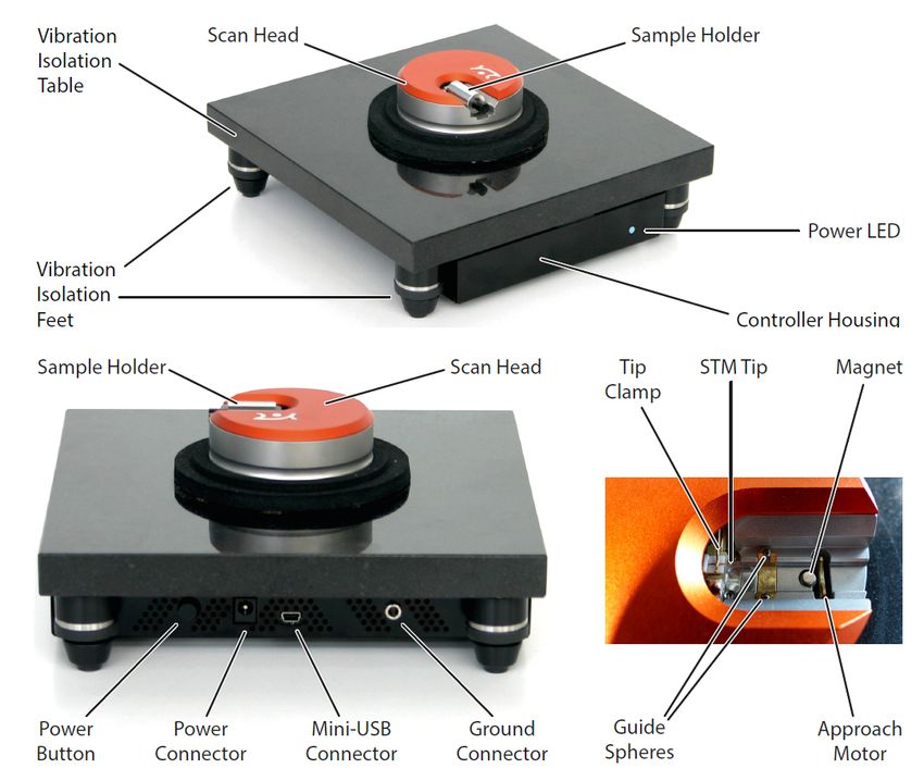
mentioned topics. The tutor
nds the following literature very helpful:
Introduction to solid state physics, C. Kittel
Solid state physics, N. W. Ashcroft, N. D. Mermin
Surface science: an introduction, K. Oura, V. G. Lifshits, etc.
Introduction to scanning tunneling microscopy, C. J. Chen
Theory of scanning tunneling microscopy, lecture note of S. Lounis
2 Surface Science
Any ensemble of matter in nature is
nite and its boundary is the surface.
Surfaces provide a hint towards the geometric and electronic properties of the
bulk and oer interesting physics and chemistry. These include for example
heterogeneous catalysis, self-assembly, surface reconstruction, surface states,
charge density waves, and adsorption. Investigations occur at the interface
of two dierent phases, which can be solid-liquid, solid-gas, solid-vacuum,
or liquid-gas. STM is capable of measuring solid-liquid, solid-gas and solid-
vacuum interfaces. In this lab course, you will have the opportunity to study
the solid-gas and solid-liquid interface. As a solid, graphite be used, which
is described in Section 2.2. But
rst, let us talk about crystallography in
two-dimension (2D).
2.1 2D crystallography
First, recall some concepts of three-dimensional crystallography. An ideal
crystal is formed by an in
nite repetition of identical groups of atoms. The
group of atoms is called the basis. The set of points to which the basis is at-
tached to is called the lattice. (crystal = lattice + basis.) Equivalently,
as a geometric abstraction, the lattice can be de
ned by three fundamental
translation vectors ~ai (i = 1, 2, 3) such that the atomic arrangement of a
crystal looks exactly the same when viewed from the points ~r and ~r0
~r0 = ~r + n1~a1 + n2~a2 + n3~a3 ,
where ni (i = 1, 2, 3) are any integers. Based on symmetry, Aguste Bravais
concluded that only 14 types of lattices exist in 3D (Bravais lattice). This
number reduces to 5 in 2D.
Any geometrical area (containing one or several lattice points) that can
tile the plane (without gaps or overlap) is a unit cell. A unit cell with
only one lattice point (i.e. minimum area) is a primitive unit cell. A
special primitive unit cells are the one spanned by the three vectors ~a1 , ~a2 ,
and ~a3 . The Wigner-Seitz cell is the one formed by drawing lines from a
given point to all others, and then constructing the perpendicular bisectors
of these lines. The smallest enclosed area around the starting point is then
the Wigner-Seitz cell (Figure 2a).
4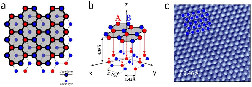
Figure 2: (a) Schematic diagram illustrating the construction of the Wigner-
Seitz cell. (b) The rst three Brillouin zones of a 2D square reciprocal lattice.

   We have seen that a crystal is invariant under any translation of the form
~
R = n1~a1 + n2~a2 + n3~a3 . Any local physical property of the crystal, such as
the charge concentration n(~r), is invariant under R    ~ , i.e. n(~r + R)
                                                                        ~ = n(~r).
(Please note that the wave function has no such invariance. Think about
why, and answer it in the report). Now recall your mathematical analysis
course (Fourier analysis), the charge concentration can be also expressed as
                                    X
                            n(~r) =            ~ · ~r),
                                      nG~ exp(iG
                                     ~
                                     G

where G ~ = v1~b1 + v2~b2 + v3~b3 , is a vector of the reciprocal lattice. The
primitive vectors ~bi (i = 1, 2, 3), are related to the primitive vectors of the
Bravais lattice as follows:
      ~b1 = 2π ~a2 × ~a3 , ~b2 = 2π ~a3 × ~a1 , ~b3 = 2π ~a1 × ~a2 .
               ~a1 · ~a2 × ~a3          ~a2 · ~a3 × ~a1      ~a3 · ~a1 × ~a2
Unlike the pure math convention you might remember, we normally include,
in solid state physics, the 2π in the reciprocal lattice vectors for convenience.
    Similar to the Wigner-Seitz cell in the real space, we can now construct
the Brillouin zones in the reciprocal space (Figure 2b). The 1st Brillouin
zone (1BZ) is then the Wigner-Seitz cell of reciprocal lattice. The introduc-
tion of reciprocal lattice and Brillouin zones comes very handy when we deal
with momentum in crystals (diraction, electronic, and thermal properties).
    In 2D, we just need to set the third primitive translation vector ~a3 to be
the normal vector n̂ perpendicular to the 2D plane (the plane ~a1 and ~a2 are
in). The reciprocal lattice vectors are

                      ~b1 = 2π ~a2 × n̂ , ~b2 = 2π n̂ × ~a1 .
                              |~a1 · ~a2 |        |~a1 · ~a2 |

2.2    Graphite

Graphite consists of carbon atoms, which form layers that are stacked on
top of each other. The carbon atoms within a layer are bound by strong

                                         5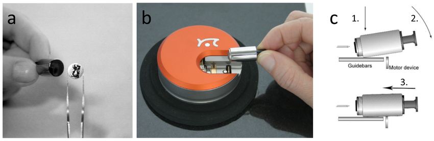
covalent bonds, while the bonding between the layers occurs via the weaker
van der Waals bond. The carbon atoms in one layer are organized in a
honeycomb lattice as shown in Figure 3a and b. Pay attention to the
values in the gures. They will be used in data analysis.

Figure 3: Atomic structure of graphite. a) Top view , b) 3D [17], c) STM
image of graphite with atomic resolution[13].

    One layer alone is called graphene, which is the prototypical 2D material,
that has peculiar electronic properties diering from graphite and for which
the Nobel prize in physics was awarded in 2010.
    Graphite is commonly used to calibrate the STM as the atoms can easily
be imaged and the surface is inert. In comparison to the naturally occurring
graphite, synthetic highly oriented pyrolytic graphite (HOPG) is used as
individual graphite crystallites are well aligned with each other. In Figure
3c a topographic image of graphite is shown. Notably, a hexagonal pattern
is visible, which diers from the honeycomb pattern. This is due to an
electronic eect that allows only every second atom to be imaged. Carbon
atoms of the surface layer, which sit on top of another atom of the second
carbon layer are not imaged as the electron density is localized closer to the
bulk [19].
    Now it is a good chance to apply the concepts mentioned in 2.1 on this
real life material with simple structure. This is left as an exercise (Section
6.1).

3    STM Basics
In STM, piezo-elements move a metal tip across the surface of a sample (see
Figure 4a). Piezo-elements change their length under an applied voltage. By
changing the voltage one can move the tip with pico-meter precision.
    The applied bias voltage drives a tunneling current through the small
distance between the tip and the sample. The scanning of the sample surface
can either be done in constant-height or constant-current mode. In the
constant-height mode the tunneling current is a function of lateral position of

                                      6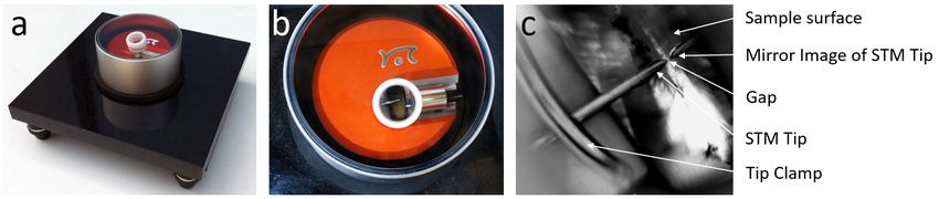
the tip. In the more commonly used constant-current mode, a feedback loop
regulates the height of the tip to keep the tunneling current constant. Thus
one obtains a pro
le of the height out of the z -signal. The good resolution
down to the atomic level is enabled by the exponential dependence of the
tunneling current on the distance (by changing the distance by one Angström
the tunneling current changes by one order of magnitude) and the precise
movement with the piezo-elements.
Figure 4: a) Scanning tunneling microscope (schematic) b) constant-current
mode shown with circuit [6].
3.1 Quantum mechanical tunneling
This section requires the students to have basic knowledge of quantum me-
chanics. If forgotten, please refer to any standard textbook (e.g. Sakurai).
In quantum mechanics, a particle with an energy lower than a potential
barrier can tunnel through the barrier because of the tunneling eect. In
classical mechanics this is not possible.
In general, energy is conserved:
Ekin + Epot = E = const
In classical mechanics the equation of motion in a one-dimensional po-
tential V (z) reads:
1 p2
mv 2 + V (z) = + V (z) = E
2 2m
The momentum p is then given by:
p
p = 2m(E − V (z))
which shows that there is no real solution if the particle energy is smaller
than the barrier E < V (z).
7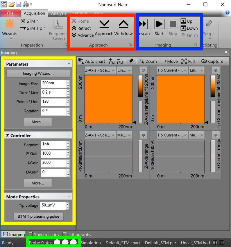
In quantum mechanics a particle can be described as a wave. This is
called the wave-particle duality. Instead of the Newtonian equation of
motion, one needs to solve the Schrödinger equation. In the 1D case, the
time independent Schrödinger equation simpli
es to:
~2 d2 ψ(z)
− + V (z)ψ(z) = Eψ(z)
2m dz 2
By rearranging one gets:
d2 ψ(z) 2m(E − V (z))
+ ψ(z) = 0
dz 2 ~2
Now we use an exponential approach ψ(z) = Ceλz to solve this equation.
This gives us two solutions for the coe
cient λ:
r
2m
λ1,2 (V ) = ± − 2 (E − V )
~
This coe
cient can either be real or imaginary, depending on the energy
of the particle and the height of the potential barrier. This means that in
contrast to classical mechanics the energy of the particle can also be lower
than the barrier. The general solution is a linear combination:
ψ(z) = A · eλ1 z + B · eλ2 z
Figure 5: Schematic of a particle tunneling through a constant potential
barrier.
Now we use a constant potential V (z) = V0 like in Figure 5 for the energy
barrier between the STM tip and the sample surface, and distinguish the
three areas. Area (I) and (III) represent the tip and the sample, respectively.
Area (II) represents the (vacuum) gap. We consider the situation where the
energy of particle is lower than the potential (E < V0 ). The solutions of
the Schrödinger equation, are obtained separately for each area with the
8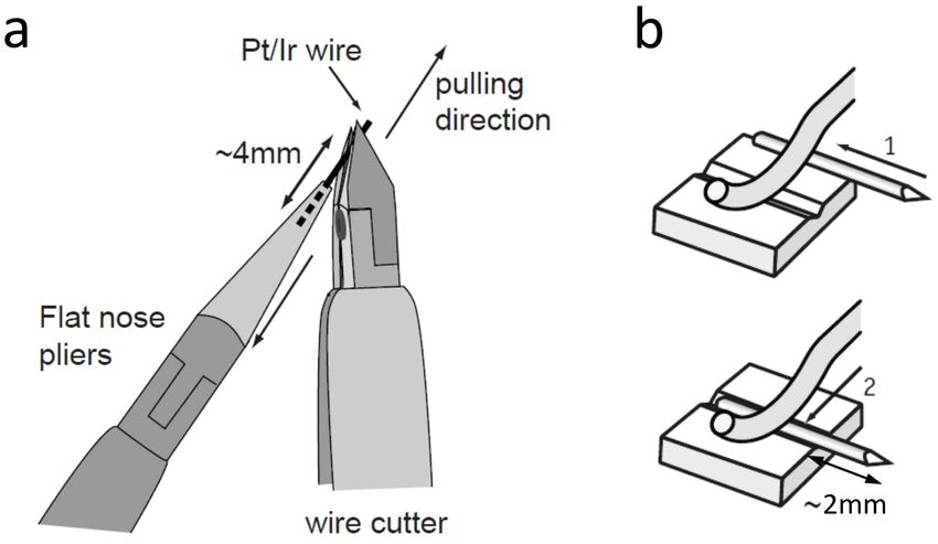
exponential approach:
√
−ikI z 2mE
I. V = 0, ψI (z) = ikI z
e } + |B · e{z
|A ·{z with kI =
} ~
incoming wave re
ected wave
p
−kII z −2m(E − V0 )
II. V = V0 , ψII (z) = C | ·e
kII z
{zD · e
+ with kII =
} ~
decaying wave function in barrier
√
2mE
III. V = 0, ψIII (z) = F ikIII z
| · e{z } with kIII = kI =
~
transmitted wave
Note that there is only the transmitted term in area (II). (In physics, do not
let the mathematical completeness formality constrain you. But at the same
time, be careful: make assumptions boldly, and then carefully justify them.)
The relation between the coe
cients A, B, C, D, and F can be calculated
from the continuity condition:
ψI (0) = ψII (0); ψII (d) = ψIII (d);
dψI (0) dψII (0) dψII (d) dψIII (d)
= ; =
dz dz dz dz
The probability of transmission is given as the transmitted particle
ow
Strans divided by the incoming particle
ow Sin . In general, the particle
ow
is the product of probability density |ψ(z)|2 and velocity v . The transmission
is then given as:
Strans |ψIII (z)|2 vIII FF∗
T = = =
Sin |ψI,in (z)|2 vI AA∗
Since the velocities vI and vIII are equal because of the constant kinetic
energy in case of elastic tunneling, one can reduce them in the fraction. For
low particle energy (E
V0 ) and wide barriers (κII d
1) the probability
of transmission simpli
es to:
√
16 −2 2m(V0 −E)d
T ≈ V0
e ~
3+ E
This derivation is not speci
ed to the type of particle. This is why also
protons or neutrons or even bigger particles can tunnel through a potential
barrier.
3.2 Tunneling current
In STM, a voltage is applied between the tip and the sample. Typically,
this voltage is in the range of -10V to +10V. Thus electrons can tunnel
9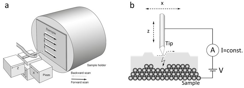
through the potential barrier, which is given by the work function of the
tip and the sample. The work function describes the minimum energy which
is needed to remove an electron from the solid and typically, it is around a
few electron-volt (eV). This current,
owing because of the tunnel eect, is
called tunneling current. It can be calculated as follows.
If we consider two
at planes and an insulating material in between,
Fermi's Golden Rule (justi
ed by the small bias voltage applied) gives the
probability of one electron
owing from one side to the other. For the current
this means:
X
I(V, T ) = 2e |Mµν |2 δ(Eµ − eV − Eν )
µ,ν
· (f (Eν − eV, T )(1 − f (Eν , T )) − f (Eν , T )(1 − f (Eµ − eV, T )))
where the sum goes over all states µ and ν of each electrode, and the tem-
perature dependent Fermi-Dirac distribution f (E, T ) of tip and sample get
multiplied with the transition matrix-elements
~2
Z
Mµν = − dS · (ψν∗ ∇ψµ − ψµ ∇ψν∗ ).
2me
Terso and Hamann have applied this model to describe the particu-
lar geometries of the STM [7]. They approximated the tip as spherical s-
wavefunction and obtained for the tunneling current:
Z ∞
I(V, T, x, y, z) ∝ dE · ρt (E − eV ) · ρs (E, x, y)
−∞
· τ (E, V, z) · (f (E − eV, T ) − f (E, T ))
where ρt is the density of states (DOS) of the tip and ρs the local density
of states of the sample and z the distance between. If we neglect parallel
components of the electron-momentum, the tunneling transmission factor τ
is given as:
p !
2 me (φt + φs − 2E + eV )z
τ (E, V, z) = exp −
~
with φt and φs as the work function of tip and sample. For low temperatures,
the Fermi-Dirac-distribution becomes a step function. This cut the integral
to only 0 eV. Furthermore, for low voltages, the dependence of the τ factor
from the voltage and energy can be neglected. These two conditions simplify
the tunneling current to:
p ! Z
eV
2 me (φt + φs )z
I(V, x, y, z) ∝ exp − · dEρt (E − eV )ρs (E, x, y)
~ 0
10The
rst term describes the exponential dependence of the current from
the distance between tip and sample. The second term is the convolution
of the density of states of the tip with that of the sample. If one applies a
positive bias voltage between sample and tip, electrons from occupied states
of the tip tunnel to unoccupied states of the sample and vice versa (see
Figure 6). Based on I(V ) curves one can distinguish between conductors
and semi-conductors. A semi-conductor has no tunneling current within the
band gap (ρs = 0), because there are no states from where electrons can
tunnel from or to.
Figure 6: Energy diagram of tip and sample in case of negative bias voltages.
Now let us take another look at this equation. When we keep the tip
still, z is a constant. And we assume the DOS of the tip is constant. We
reach
dI
(V, x, y) ∝ ρs (eV, x, y)
dV
Thus by measuring the derivation of the current with respect to the
voltage, which mostly is measured by a lock-in-ampli
er, we have a way
to detect the DOS of the sample. This is called the scanning tunneling
spectroscopy (STS). One should notice the tip can only interact with the
electrons in a very small area of the sample surface (exponential decay by
distance). Thus STS actually measures the local density of states (LDOS).
The energy resolution is given by pthe temperature and the modulation
amplitude of the voltage as ∆E ≈ (3kB T )2 + (2.5eVmod )2 . The thermal
broadening increases with the temperature and hence the energy resolution
decreases, e.g. at room temperature (T ≈ 300K) the energy resolution is
around 80 meV but at low temperatures (T ≈ 4.2 K) around 1 meV.
The exponential decay of the tunneling current with increasing distance
between tip and sample depends on the material. By measuring the tunneling
current while changing the distance, i.e. I(z), one obtains information about
the height of the potential barrier. When keeping the bias voltage constant,
and the tip still in x and y directions, one obtains:
p !
2 me (φt + φs )z
I(z) = C · exp −
~
11and with the natural logarithm this becomes:
p
2 me (φt + φs )z
ln(I(z)) = ln(C) − = ln(C) − κ · z
~
The value of κ, which describes the exponential decay of I(z), is given as:
p
2 me (φt + φs )
κ=
~
This means that the mean value of the potential barrier height φb can be
obtained by measuring κ, the slope of the ln(I(z)) curve:
φt + φs κ2 ~2
φb = =
2 8me
4 Experimental Setup
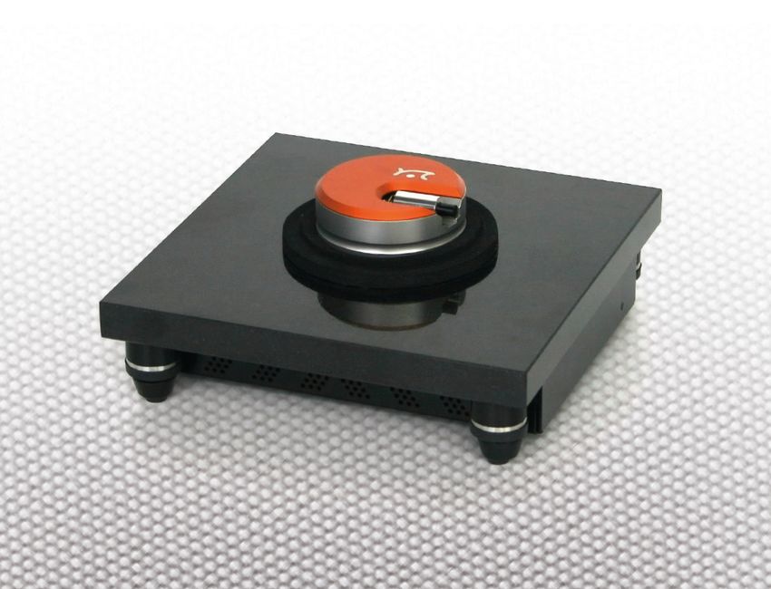
Figure 7: Setup of the NaioSTM [11].
The STM used in this lab course is the NaioSTM from Nanosurf (see
Figure 7). It mainly consists of the scanning part colored in orange and
a table for vibration isolation. There is also a cover for protection with a
magni
er to check tip and sample. The product video [10] provides a good
introduction to the setup and the functionalities. Further information about
the instrument can be taken from the user manual of the company [6, 11].
The measurements are done by giving commands in the controlling software.
12This STM is located in ENC B-0132. The machine is mainly for lecturing
purpose. Thus it is at ambient environment. In the same room, there is
another STM machine for research usage. It is mounted in an ultra high
vacuum chamber (UHV, crucial to surface science study). Please do not
temper with this machine during the lab course.
5 Experimental Instructions
In the lab, the most important thing is to protect the safety of yourself,
especially since we're dealing with some harmful chemicals. Also, STM is a
quite delicate setup, so be gentle with it.
Bearing these two points in mind, you need to
nish the following tasks
during the lab course, which are explained with more detailed instructions
in the latter sections:
1. Prepare your own tip, and mount it into the setup.
2. Scan on HOPG surface in air, and get both large size image (∼ 100
nm) presenting the step edges, and small size image (∼ 5 nm) with
atomic resolution.
3. Calibrate the distortion on the atomically resolved HOPG image, and
get the distortion parameters for later usage.
4. Prepare the solution of organic molecules and apply it to the HOPG
surface.
5. Scan on the HOPG again, now this time at a liquid/solid interface,
and try to get atomic resolution on the organic molecules.
6. Calibrate the molecule images with the distortion parameters obtained
from the HOPG images.
The STM can do much more than the things the tutor listed here. If we
have time and you're interested, we can try some other things. It might also
be possible to take a look at what is going on at the other research STM in
the same room.
5.1 Preparing and installing the STM tip
The STM tip can be prepared out of Pt/It wire and installed by yourself.
This is the most di
cult part of the preparation which has to be carried our
very thoroughly. It usually needs patience and practice to get the
rst good
tip. A good tip is very sharp but not too long or bent. Only an accurately
cut tip enables optimal measurements. Preparing and installing should be
carried out with great care.
13Before preparing the tip
1. Wear gloves to avoid any contamination oil from the skins.
2. Clean the cutting part of the wire cutters, the
at nose pliers and the
pointed tweezers with isopropanol. Only touch the Pt/Ir wire with
these tools.
3. Remove any remaining tip from the instrument using the pointed
tweezers just by pulling it out of the tip holder in the STM.
Prepare the tip
1. Hold the end of the wire tightly with the pliers.
2. Holding the wire with the pliers, move the cutters at a wire length of
approximately 4 mm, as obliquely as possible (in a very sharp angle,
see Figure 8a).
3. Close the cutters until you can feel the wire, but do not cut the wire.
4. In order to obtain the required sharpness, the tip needs to be torn o
by pulling the wire cutter quickly away from you, rather than cutting
cleanly through the wire.
5. Use the pointed tweezers to hold the tip wire right behind the tip and
release the
at pliers.
Figure 8: Preparation and installation of the STM tip: a) cutting, b) mount-
ing [11].
Now that you have prepared a fresh tip it is necessary to handle it with
care. It is important that you never touch the end of the tip with anything.
14Mount the STM tip
Figure 8b shows the tip holder with its groove and the clamp which
xes the
tip wire.
1. Put the tip wire underneath the clamp of the tip holder, parallel to
the groove and push the blunt end of the tip all the way to the end.
2. Move the tip wire sideways until it is in the groove and held securely
under the clamp. It should stick out about 1-2 mm beyond the tip
holder.
The tip is now installed and you can go on preparing the sample.
5.2 Prepare and mount the sample
Cleave the HOPG
At
rst you will test your tip on HOPG. Therefore you need to cleave the
HOPG sample once with a piece of adhesive tape (Tesa
lm) as shown in
Figure 9 and explained in the following:
1. Leave the sample
xed on the magnetic stripe in its storing box.
2. Stick a piece of adhesive tape to the graphite surface and apply little
pressure with your thumb or the end of the tweezers.
3. Pull o the adhesive tape gently. The topmost layers of the sample
should stick to the tape.
4. The surface should be very
at and mirror-like. Any loose
akes in the
outer regions of the sample can be removed with the tweezers.
Figure 9: Cleaving graphite with a adhesive tape [11].
Mounting the sample Now you need to put the sample into the setup.
The procedure is shown in Figure 10.
1. Unpack the shuttle touching only its black plastic handle. This is very
important, because otherwise a grease
lm on the shuttle will prevent
the motor device to move the sample.
152. Use the tweezers to push the sample to the edge of the supporting
magnet in the sample storing box. Grab the sample with the tweezers
and place it on the magnet of the shuttle.
3. Put the shuttle down to the shuttle guide bars
rst and release it gently
on to the magnet of the approach motor.
4. Push the shuttle carefully in the direction of the tip (until the distance
is around 3 mm), but do not let it touch the tip.
5. Put back the cover of the setup, and adjusting the position of the
magni
er
Figure 10: Mounting the sample [11].
5.3 Approach
To approach the sample to the tip you need to use the Nanosurf Naio soft-
ware. Therefore you need to switch on the NaioSTM by pushing the power
button, and start the software on the computer. With the button Advance
(see the red box in Figure 11) you move the shuttle towards the tip. To check
the distance, you may look through the magni
er as shown in Figure 12. At
a certain distance one can see the mirror image of the tip in the sample.
Now you can approach a little bit more till the gap between the tip and the
sample is very small (1 mm or even closer). The smaller it is, the less time
the automatic
nal approach needs. To start the automatic
nal approach
you can click on the button Approach. Now the computer approaches the
sample step by step, checking the tunneling current each time and stopping
the approach when the set-point is reached. In this case, the Probe Status
shown in the green box in Figure 11, turns to green.
In case that the automatic approach crashed the sample into the tip, it
turns to red and you probably need to prepare a new tip. Therefore you
click Withdraw once and afterwards Retract several times. Now the gap
should be wide enough to unmount the tip. If the automatic approach is not
working at all, you should click Withdraw and Retract, rotate the shuttle
a bit and start a new approach as explained above. If this still does not
work, you will need to clean the metallic part of the shuttle with ethanol.
16Figure 11: User interface of the Naio software in version 3.8
5.4 Constant-current mode scan
The scanning starts automatically after the approach. It can be stopped or
paused any time by clicking the respective buttons in the blue box of Figure
11. In the panels Parameters, Z-Controller and Mode Properties the
most important scan parameters can be changed. You will
nd them in the
yellow box of Figure 11.
Image Size De
nes the image size in the x and y direction. You
should
rst scan a large area (100 200 nm), and then zoom in the
interested small areas step by step.
Time/line The time needed to acquire a single data line. The time
needed for the entire image is displayed in the status bar. Normally,
you choose a time as short as possible to save time, but especially for
steps at the end of a terrace this could trigger problems, because the
feedback loop, which controls the tip position in z -direction, may not
be able to retract fast enough and the step becomes blurred or the tip
crashes the sample.
17Figure 12: a) glass cover with magni
er, b) top view, c) gap between tip and
sample [11].
Set-point The working point for the z feedback loop, which de
nes at
which tunneling current the tip is held. This essentially determines the
distance between tip and sample. The higher the set-point, the closer
the tip is held above the samples surface. For example, for atomic
resolution on graphite you normally use 5 nA. A good value to start
with is typically 1 nA.
P-, I-, D-Gain P-proportional, I-integral and D-derivative controller
are the values of the feedback loop. They de
ne the strength of the
reaction if the measured current diverges from the Set-point. Values
too small could cause the tip to no longer react accurately to changes
in altitude. Values too big could cause oscillations of the tip position.
Typically, you can set D to zero. P and I need to be chosen in accor-
dance to the current and time/line. The default value 1000 is a good
starting point.
Tip voltage This parameter de
nes the bias voltage applied to the
tip. The lower the voltage is, the shorter the distance between tip
and surface becomes. A good bias voltage value largely depend on the
electronic structure of the sample, i.e. DOS(E). For semiconductors it
is important to note that the applied bias voltage is not recommended
to be in the band gap. Think about why, and answer it in the report
(see Section 6.1).
5.5 Arachidic acid on graphite
Organic molecules are the conceptional, structural, and functional basis
of numerous existing and envisaged nanotechnology applications, such as
molecular light-emitting and harvesting devices, molecular electronics, bi-
ological identi
cation, and molecular sensor technologies. Because devices
based on single molecules are still challenging for applications, systems in-
volving molecular thin
lms appear to be the most promising for the near
future. Self-assembly is one of the major routes toward novel molecular
architectures and is used, for instance, for the realization of electronic and
optoelectronic devices.
18You need to wear gloves again (and eye-shield), but this time it is for
your own safety from the harmful organic compounds. Do not deliberately
inhale any organic compound. And if you touch the solution with bare skin,
remain calm, and wash thoroughly with soap.
Prepare the solution In this experiment we will investigate the adsorp-
tion of arachidic acid on HOPG. For this one needs to set up a saturated
solution of arachidic acid in phenyloctane. This is done by the tutor already.
Apply the solution To apply the molecules to the surface
rst stop the
measurement on HOPG when seeing single atoms.
1. Withdraw the sample via the Withdraw button, and retract the sam-
ple once with the Retract button. Remove the cover from the STM
carefully.
2. Use the syringe with the smallest (brown plastic top) needle, or a
pipette, to aspirate a small volume of the thinned down arachidic acid
solution.
3. Push its piston a bit, such that a drop of the solution adheres to the
top of the needle.
4. Now touch the HOPG surface near the tip with the drop carefully.
The drop will come undone the needle and disperse across the sample
resulting in a liquid meniscus between the scanning tip and the sample
as shown in Figure 13a. Now we have a liquid-solid interface.
Figure 13: (a) A meniscus forms between the tip and the HOPG [11]. (b)
Uncalibrated STM image of arachidic acid molecules on HOPG (0.6 nA, 1.3
V, image size 15.8× 15.8 nm2 ).
Please be very careful with the solution, and do not drop any super
uous
liquid into the setup.
19Scan again Now place the cover carefully on the STM again. The status
light should be orange all the time. Approach the sample like on the HOPG
again, and you should be able to see the atomic resolution of HOPG as
before. If not, try scanning a dierent area of the surface (lower resolution
move increase resolution on
at terrace).
If you are not able to achieve atomic resolution, you probably have
crashed the tip into the sample when applying the solution. Hence you
will have to prepare a new tip and start over again.
If successful, you should see some very obvious features from the Arachidic
acid (Figure 13b). And on a good day, you could even distinguish individual
carbon atoms.
5.6 Data analysis
The raw data for the surface topography image captured with the STM is in
.nib format, and consists of a matrix with a size matching the points per line
and lines per frame. The measured values get stored and encoded as 16-bit
signed integers in a value range from -32768 to 32767. With a calibration
on a well known surface the software converts these values in physical units
of a length. To display the matrix in a meaningful way, a color scale is
assigned to the measured values, where each color value represents a dierent
z -expansion of the piezo. Choose a color scale you like.
In the following some image processing steps are explained using the free
software Gwyddion [8]:
Fast-Fourier-Transformation (FFT): This option is given in the drop
down menu Data Process/Integral Transforms/2D FFT. The
software will do a Fourier transformation of the whole picture. In
the resulting reciprocal space one can see periodic signals, which for
example come from the periodic structure of the atoms in a crystal or
noise. With the option Process/Correct Data/2D FFT Filtering
it is possible to cut out the noise and transform the picture back in
real space, where its now
ltered from the noise. In reciprocal space it
is also possible to determine the atomic distance.
Distortion calibration: In principle, what the machine can read from
the measurement is only electric signals (voltage, current ...). The
STM electronics translates them to dimensions (length in x, y , and
z directions). These values might not be accurate. We need to cal-
ibrate them with the known dimensions. In drop down menu Data
Process/Distortion/A
ne, we calibrate our measured HOPG im-
age against the HOPG crystal structure in stored already in the soft-
ware. You just need to make sure the
t lattice mapped on the image
is correct. Then you press OK, and the software will generate a cali-
brated image.
20 Line pro
le: This option is given in the Data Process box, the Ex-
tract Pro
le button. Draw a line on the image, and the software will
plot the pro
le of height along this line. This is very practical to get
the height of a step or to count the atoms along a line with a known
length to determine the atomic distance.
Smooth: Gwyddion gives an option to smooth the picture. It is given in
the Tool box, the basic
lter button. There are several
lters available,
and you can enter the size of area you want to smooth. You can use
Gaussian
lter and a size of 2-5 pixels, and press apply button. But
note that an average over a big number of pixels will lead to information
loss. You should distinguish the real physics information, and the
background noise, and use this function.
The program has many more options which are not discussed here. You are
free to test this on your own. There is another free software you can give a
try. WSxM [12] gives very similar functions as Gwyddion. But some
nd it
more user-friendly.
6 Report
6.1 Exercise
Answers to the following questions should be included in the report. If
they are already explained in other part in your report (especially the
fth
question), there is no need to repeat.
1. What is the Bravais lattice of graphite and graphene? Draw the unit
cells, and label the primitive translation vectors.
2. Calculate the reciprocal lattice vectors of graphene, and draw the 1BZ
of graphene. Label all the high symmetry points in 1BZ.
3. Why is wave function not invariant under lattice translation?
4. Why is the bias voltage not recommended to be set within the band
gap if the sample is a semiconductor?
5. What is the reason for the arachidic acid molecules to self-assemble?
Elaborate on the inter-molecular interactions.
6.2 Requirements
The report should cover things you have done before, during, after the exper-
iment, and what you have learned through the process. In principle, there
is no compulsory format. But please make it organized. If you have have no
idea, here are some suggested sections:
21 Introduction for what the lab course is about, what you have learned,
how your report is constructed.
Theory for the background information behind this experiment. The
theory part about the spectroscopy (and organic molecules) is rather
brief in this manual, please elaborate in your report.
Experimental for brie
y description of the setup and procedure.
Result to exhibit the experimental results and your analysis. Specify
the data analysis process for the presented STM images. Make sure
every STM image is accompanied by the length scale indication, and
the tunneling parameters (check the STM image in this manual, or
STM images in any academic articles for example). The systems we
measured have already been studied before, please take the existing
articles for references, and compare the results you measured with the
ones in literature.
Summary.
Exercise to answer the questions in Section 6.1 of this manual.
The theory and experimental part should not be a simple repetition of the
same section of this manual. Please use your own words.
References
[1] G. Binnig, H. Rohrer "Scanning tunneling microscopy" Surface Science
126, 236 (1983)
[2] J. Coraux, A. T. N'Diaye, C. Busse, T. Michely "Structural coherency
of Graphene on Ir(111)" Nano Letters 8, 565 (2008)
[3] https://www.ru.nl/spm/research/imagegallery/
[4] D. M. Eigler, E. K. Schweizer "Positioning single atoms with a scanning
tunneling microscope" Nature 344, 524 (1990)
[5] R. Ohmann, J. Meyer, A. Nickel, J. Echeverria, M. Grisolia, C. Joachim,
F. Moresco, G. Cuniberti "Supramolecular Rotor and Translator at
Work: On-Surface Movement of Single Atoms" ACS Nano 9, 8394
(2015)
[6] "PHYWE Operating Instructions and Experiments Scanning Tunneling
Microscope (STM)"
https://repository.curriculab.net/files/bedanl.pdf/09600.
99/e/01192_02.pdf
22[7] J. Terso, D. R. Hamann "Theory of the scanning tunneling micro-
scope" Phys. Rev. B 31, 805 (1985)
[8] D. Necas, K. Petr "Gwyddion: an open-source software for SPM data
analysis." Open Physics 10.1 (2012).
[9] R. Gross, A. Marx "Festkörperphysik" Oldenbourg Wissenschaftsverlag
GmbH (2012)
[10] "Compact STM, Rastertunnelmikroskop"
www.youtube.com/watch?v=SmhUmY8a0wI
[11] "NaioSTM Operating Instructions for Naio Control Software Version
3.8"
[12] WSxM: A software for scanning probe microscopy and a tool for nan-
otechnology
www.wsxm.es
[13] Homepage Firma Nanosurf
www.nanosurf.com
[14] Annalen der Physik: 5.Folge, Band 4, Heft 2, 1930
[15] http://www.apmaths.uwo.ca/~mkarttu/CDW/ (21.09.18)
[16] http://www.pro-physik.de/details/news/2493101/
Konstruktiver_Konflikt_im_Supraleiter.html (15.10.18)
[17] Advanced Integrated Scanning Tools for Nano Technology
http://nanoprobes.aist-nt.com/apps/HOPGinfo.htm
[18] Tantalum (IV) sul
de wikipedia article
https://en.wikipedia.org/wiki/Tantalum(IV)_sulfide
[19] S. Hembacher, F. J. Giessibl, J. Mannhart, and C. F. Quate "Reveal-
ing the hidden atom in graphite by low-temperature atomic force mi-
croscopy" PNAS 100, 12539 (2003)
http://www.pnas.org/content/100/22/12539
[20] F. Joucken, F. Frising, R. Sporken "Fourier Transform Analysis of STM
Images of Multilayer Graphene Moiré Patterns" Carbon 83, 48 (2015)
[21] J. Fuhrmann "Aufbau eines Rastertunnelmikroskops unter Umgebungs-
bedingungen" (2018)
23You can also read