Two-dimensional ferroelectric channel transistors integrating ultra-fast memory and neural computing
←
→
Page content transcription
If your browser does not render page correctly, please read the page content below

ARTICLE
                  https://doi.org/10.1038/s41467-020-20257-2                 OPEN

                  Two-dimensional ferroelectric channel transistors
                  integrating ultra-fast memory and neural
                  computing
                  Shuiyuan Wang1, Lan Liu1, Lurong Gan1, Huawei Chen1, Xiang Hou1, Yi Ding1, Shunli Ma1, David Wei Zhang1 &
                  Peng Zhou 1 ✉
1234567890():,;

                  With the advent of the big data era, applications are more data-centric and energy efficiency
                  issues caused by frequent data interactions, due to the physical separation of memory and
                  computing, will become increasingly severe. Emerging technologies have been proposed to
                  perform analog computing with memory to address the dilemma. Ferroelectric memory has
                  become a promising technology due to field-driven fast switching and non-destructive
                  readout, but endurance and miniaturization are limited. Here, we demonstrate the α-In2Se3
                  ferroelectric semiconductor channel device that integrates non-volatile memory and neural
                  computation functions. Remarkable performance includes ultra-fast write speed of 40 ns,
                  improved endurance through the internal electric field, flexible adjustment of neural plasticity,
                  ultra-low energy consumption of 234/40 fJ per event for excitation/inhibition, and thermally
                  modulated 94.74% high-precision iris recognition classification simulation. This prototypical
                  demonstration lays the foundation for an integrated memory computing system with high
                  density and energy efficiency.

                  1 ASIC   & System State Key Lab., School of Microelectronics, Fudan University, Shanghai 200433, China. ✉email: pengzhou@fudan.edu.cn

                  NATURE COMMUNICATIONS | (2021)12:53 | https://doi.org/10.1038/s41467-020-20257-2 | www.nature.com/naturecommunications                  1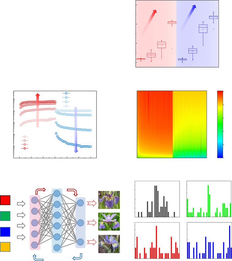
ARTICLE                                                                 NATURE COMMUNICATIONS | https://doi.org/10.1038/s41467-020-20257-2

T
        he rise of artificial intelligence has led to explosive growth         color atomic force microscope (AFM) amplitude error image of
        in emerging data-centric applications represented by                  the 2D FeCTs. And the detailed thickness information of α-
        images recognition and classification1,2. Data-intensive               In2Se3, bottom h-BN and top h-BN measured by AFM is pro-
tasks require computing systems to perform batch parallel pro-                vided in Supplementary Fig. S3a in Supplementary Information,
cessing, frequently accessing results and interacting from memory             which are approximately 40 nm, 20 nm and 20 nm, respectively.
domains3. The computing and memory components of modern                       In addition, the high-resolution scanning transmission electron
computers are physically separated4, and massive communication                microscope (STEM) was used to characterize and observe the 2D
increases unexpected power consumption and degrades effi-                      FeCTs microstructure. The cross-sectional image and corre-
ciency, causing the so-called von Neumann bottleneck5.                        sponding energy dispersive X-ray spectroscopy (EDS) element
   Emerging memory devices such as memristors6, memtransis-                   mapping at the interface between the multilayer h-BN and α-
tors7, phase change memory8, electrical double-layer transistors9,            In2Se3 are shown in Fig. 1c, which implies a clean van der Waals
two-dimensional (2D) heterojunction devices10, and ferroelectric              heterojunction with negligible interface state trapping effect.
field effect transistors (FeFETs)11 are used to perform analog                 Figure 1d shows the Raman spectrum of the channel α-In2Se3 to
computation in an attempt to break out of the dilemma. FeFETs                 characterize the material properties, which is consistent with
with switchable electric dipoles, fast operation12,13 and non-                previous reports14,18,30. It is worth noting that the additional
destructive readout14 are ideal for building low-power12, high-               splitting peak near 90 cm−1 can be regarded as an indication of
efficiency memory computing integrated systems. However, tra-                  hexagonal (2H) stacking18. To further confirm the 2H structure,
ditional FeFETs use ferroelectrics as the dielectric layer to mod-            we have supplemented the X-ray diffraction (XRD) character-
ulate channel conductance14. The residual polarization decreases              ization of α-In2Se3 crystals, as shown in Supplementary Fig. S2.
with cumulative switching cycles, and ferroelectric fatigue                   The diffraction pattern only shows the c-plane peak and its
occurs15, resulting in memory with limited endurance16.                       higher-order interplanar spacing. The peak pattern can determine
   In addition, the future trend of high-integration artificial intel-         the lattice constant c (≈19.23 Å), which is consistent with the
ligence applications is pushing the design of memory and com-                 reported 2H α-In2Se3, and is significantly different from 3 R α-
puting elements toward miniaturization17,18. Bulk perovskite19,               In2Se331–33. And the Raman characterization of h-BN is shown in
oxide11,20, or organic ferroelectric polymer21 are served as the gate         Supplementary Fig. S3b in Supplementary Information. Crucially,
dielectric in conventional FeFETs, which is insufficient for con-              we transferred the 40 nm channel α-In2Se3 ferroelectrics onto a
tinuous scaling both in vertical and planar dimensions22. 2D                  conductive Au/Al2O3 substrate and determined its ferroelectric
layered semiconductors with atomic thickness possess the potential            polarization by piezoelectric microscopy (PFM). Figure 1e shows
for continuous shrinking23–25, which is a promising candidate for             the three-cycle off-field PFM amplitude hysteresis loop of the 40
future high-density memory and computing systems26,27. Parti-                 nm channel α-In2Se3, and the inset includes a schematic of PFM
cularly, 2D layered α-In2Se3 exhibits robust ferroelectricity at room         test structure and the PFM phase hysteresis loop (the on-field
temperature (RT) without annealing14,28,29, and thanks to the                 PFM amplitude and phase hysteresis loops are shown in Sup-
intrinsic interlocking of dipoles in α-In2Se318,22, it can maintain           plementary Fig. S4), which indicates a significant ferroelectric
ferroelectric polarization even at atomic scale.                              polarization flip. Figure 1f records the phases of the outer rec-
   Here, distinct from the conventional FeFETs, 2D ferroelectric              tangular track and inner square scanned on the same α-In2Se3 by
semiconductor α-In2Se3 was exploited as the channel materials to              PFM domain engineering with applying +8 V and −8 V bias to
demonstrate a compact scalable device that integrates non-                    the conductive probe respectively. The strong PFM phase contrast
volatile memory (NVM) and neural computing functions. 2D α-                   in the electrical writing region visually shows the polarization
In2Se3 ferroelectric channel transistors (FeCTs) show absorbing               reversal occurring in the channel α-In2Se3.
performance, including NVM large memory hysteresis windows,                      First, we compare traditional FeFETs with 2D α-In2Se3 FeCTs,
long-term retention, enhanced endurance by internal electric                  as shown in Fig. 2a, b. It is worth emphasizing that there is only
field, fast write speed of 40 ns, flexible adjustment of neuroplas-             polarization bound charges in the FeFETs14, which is reversed to
ticity and ultra-low power consumption of 234/40 fJ per event for             achieve polarization switching, and finally modulate channel
excitation/inhibition. Moreover, 2D FeCTs exhibit thermal tun-                conductance (Fig. 2a). In contrast, 2D α-In2Se3, as ferroelectric
ability in both memory and neural computation, and based on                   semiconductors34, have mobile charges as the nature of semi-
FeCTs, a simulated iris recognition and classification with the best           conductor in addition to polarized bound charges14. When 2D α-
accuracy of 94.74% comparable to the software is realized. The                In2Se3 FeCTs in the polarization-up state, positive and negative
elaborate prototype devices pave the way for building high-den-               polarized bound charges are distributed on the upper and lower
sity, energy-efficient memory and computing fusion systems,                    surfaces of the channel, respectively, shown in Fig. 2b. Therefore,
providing promising candidates for eliminating the physical                   positive and negative movable charges are accumulated on the top
separation of memory and computing.                                           and bottom surfaces of the channel, forming an upward built-in
                                                                              electric field to maintain the polarization-bound charge, which
                                                                              indicates long retention time and improved endurance of NVM.
Results                                                                       Next, we discuss the working mechanism. For convenience, we
Figure 1a shows the schematic of 2D FeCTs, which integrates                   omit the interface optimization h-BN, and only discuss the band
memory and computing capabilities, that is, non-volatile memory               bending caused by polarized bound charges in the channel,
and neural computing. 30 nm Al2O3 is deposited on the substrate               without considering the mobile charges, which is consistent with
by atomic layer deposition (ALD) as the bottom dielectric layer,              the complete theory considering both ferroelectric and semi-
and the bottom h-BN was prepared by mechanical exfoliation for                conductor properties14. Note that the gate dielectric of fabricated
interface optimization, followed by the transfer of the exfoliated            2D FeCTs has a high equivalent oxide thickness (EOT) and the
2D α-In2Se3 channel layer. Then we transfer h-BN as the top                   electric field along the channel is not strong enough, resulting in
dielectric layer, electron beam lithography forms the electrode               incomplete polarization switching and localized mobile charges
pattern, electron beam evaporation deposits the source drain and              distribution. GG applies a negative voltage (below coercive vol-
the top gate (TG), while heavily p-doped silicon substrate as the             tage), the bottom channel distributes positive polarization bound
global gate (GG) (detailed process flow shown in Supplementary                 charges, the energy band bends downward, and accumulates
Fig. S1 in Supplementary Information). Figure 1b shows the false              electrons, which forms a low resistance state (LRS ”1”),

2                NATURE COMMUNICATIONS | (2021)12:53 | https://doi.org/10.1038/s41467-020-20257-2 | www.nature.com/naturecommunications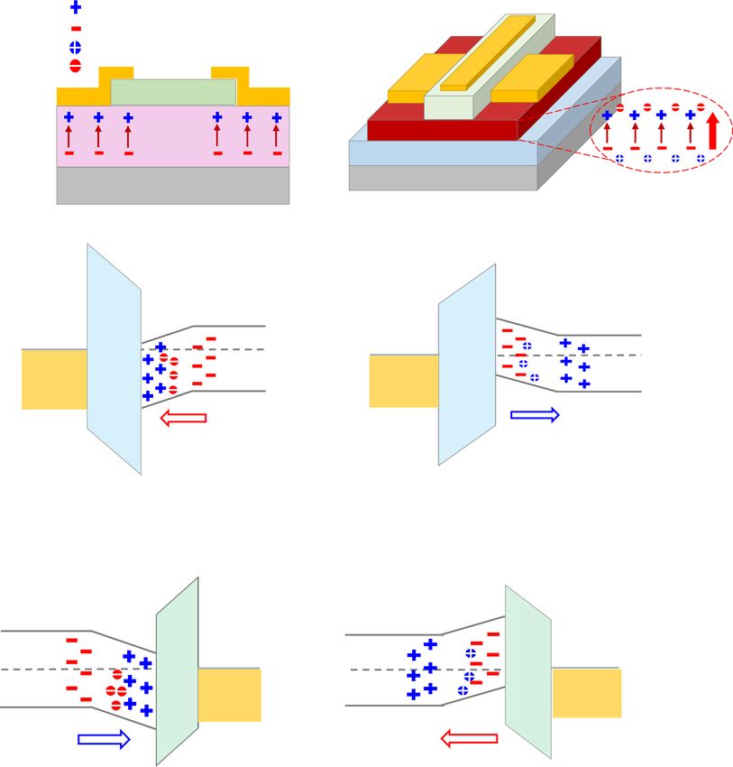
NATURE COMMUNICATIONS | https://doi.org/10.1038/s41467-020-20257-2 ARTICLE
(a) (b)
Neural Computing
Source
α-In2Se3 Top Gate Top Drain
Computation Post-
synaptic
Gate
Source Drain Pre- neuron
synaptic
h-BN neuron
Al2O3
Memory
Global Gate P++ Si
α-In2Se3
Non-volatile Memory
h-BN
(c) (d)
α-In2Se3
105 cm-1
Raman intensity (a.u.)
h-BN
89 cm-1
181 cm-1
147 cm-1 194 cm-1
α-In2Se3
10 nm
60 120 180 240 300
Raman shift (cm-1)
(e) (f)
250
200
Phase (°)
150
100
Amplitude (a.u.)
50
0
-15 -10 -5 0 5 10 15
PFM tip
α-In2Se3
Au
-15 -10 -5 0 5 10 15
Bias (V)
Fig. 1 Schematic and characterization of 2D α-In2Se3 FeCTs for memory and computing. a The 2D FeCTs structure integrates memory and computing
functions, in which α-In2Se3 ferroelectrics serve as channel layer, Al2O3 and hBN as the global and top dielectric layers respectively. Non-volatile memory is
implemented by GG, and neural computing is realized simultaneously with combination of TG. b False color AFM amplitude error image of the 2D FeCTs.
Sacle bar: 6 μm. c High-resolution STEM image of multilayer h-BN and α-In2Se3 heterojunction and corresponding EDS element mapping in FeCTs, which
indicates a clean interface. Sacle bar: 10 nm. d Raman characterization of α-In2Se3, where the 89 cm−1 peak position suggests a hexagonal structure. e The
three-cycle off-field PFM amplitude hysteresis loop of the channel α-In2Se3, the illustration includes the test structure and the PFM phase hysteresis loop,
which shows a clear ferroelectric polarization flip. f The phase image after writing the outer rectangular track and inner square by applying +8 V and −8 V
bias to the α-In2Se3 through PFM. Sacle bar: 200 nm.
corresponding to the polarization down (Fig. 2c). Conversely, polarization is formed, that is, long-term potentiation, and vice
GG applies a positive voltage (above coercive voltage), the versa. In this way, 2D FeCTs show the coexistence and evolution
negative polarization bound charge is distributed at the bottom of volatile and nonvolatile, which is exactly what neural com-
of channel, energy band bends upward, and the electrons are puting expects to simulate the short- and long-term plasticity in
depleted, which results in a high resistance state (HRS “0”) biology3,6. The energy band of 2D α-In2Se3 FeCTs under
corresponding to polarization up (Fig. 2d). The working dynamic equilibrium is shown in Supplementary Fig. S5.
mechanism of TG is similar to GG as exhibited in Fig. 2e, f, but it Figure 3a shows the 2D α-In2Se3 FeCTs transfer curves under
is worth mentioning that the coverage area of the gate to the varying bidirectional scanning voltages, where the source-drain
channel directly affects the modulation performance. Although voltage (Vds) is fixed at 1 V, and the clockwise hysteresis memory
the top dielectric (h-BN) has a lower EOT and induces a stronger windows enlarge with the incremental GG voltage (VGG)
electric field, the top electric field does not completely cover the sweeping, showing the accumulation of ferroelectric channel
channel, resulting in a weaker polarization of the channel fer- polarization switching (Supplementary Fig. S6a exhibits the out-
roelectric and depolarization in a short time. Channel con- put curves under varying VGG). Figure 3b extracts the memory
ductance returns to its initial state, showing short-term plasticity, windows, showing a maximum window of 6 V under −8 to 8 V
and negative voltage shows conductance increase (LRS “1”), sweeping. Under sufficient GG write and erase spikes (±8 V, 10 s
corresponding to short-term potentiation. However, with the and read at VGG = 0 V, Vds = 1 V), the retention characteristics
accumulation of negative voltage pulses, the channel ferroelectric of FeCTs show stable non-volatile, with high and low states
polarization is strengthened, and finally a non-volatile exceeding 103, as shown in Fig. 3c. The basic erase (LRS) and
NATURE COMMUNICATIONS | (2021)12:53 | https://doi.org/10.1038/s41467-020-20257-2 | www.nature.com/naturecommunications 3ARTICLE NATURE COMMUNICATIONS | https://doi.org/10.1038/s41467-020-20257-2
(a) (b) 2D FeCTs
Polarization Traditional FeFETs
bound charges
Mobile charges
S D
S Channel layer D
hBN
With polarized Ferroelectric
field only 2D Ferroelectric Channel E
Dielectric
(red arrow) Dielectric
Gate Global gate
With additional
built-in field
(red bold arrow)
(c) (d)
Al2O3 α-In2Se3 α-In2Se3
Negative Al2O3
Voltage Positive
Voltage
Global Global
gate gate
Polarization Polarization
down up
LRS: low resistance state LRS “1” HRS: high resistance state HRS “0”
(e) (f)
α-In2Se3 α-In2Se3
Negative Positive
h-BN Voltage h-BN Voltage
Top Top
gate gate
Polarization Polarization
up down
LRS “1” HRS “0”
Fig. 2 Comparison of FeFETs and FeCTs structure and working mechanism. a For FeFETs, traditional ferroelectrics act as the dielectric layer, where only
polarization-bound charges exist, and channel conductance is modulated by polarization switching. b The ferroelectric semiconductor 2D α-In2Se3 in FECTs
serves as the channel layer and has both polarized bound charges and mobile charges. When in a polarized upward state, positive and negative polarized
bound charges are distributed on the top and bottom surfaces of the channel, respectively, which causes positive and negative mobile charges to
accumulate in opposite positions, forming an upward built-in electric field to maintain upward polarization. c For GG, a negative voltage lower than the
coercive voltage is applied, and the bottom channel distributes positive polarized bound charges, the energy band is bent downward, and electrons are
accumulated to form LRS, which corresponds to downward polarization. d When GG applies a positive voltage higher than the coercive voltage, the
negative polarized bound charges are distributed at the bottom of the channel, and the energy band bends upward. The depletion of electrons results in
HRS, which corresponds to the upward polarization. e Similarly, for TG, a negative voltage is applied, the top channel distributes positive polarized charges,
and electrons accumulate to form LRS, which corresponds to polarization up. f A positive voltage applied in TG, the top channel distributes negative
polarized bound charges, and electrons are depleted to form HRS, corresponding to polarization down. It should be noted that owing to the high EOT of
FeCTs gate dielectric and the insufficient electric field along the channel, incomplete polarization switching and localized mobile charges distribution are
caused.
write (HRS) characteristics of NVM are described in Fig. S7a. as the write width decreases, but it is worth noting that 40 ns can
Thanks to the nature of α-In2Se3 semiconductors, the existence of still be effectively written, as shown in Fig. 3e, which is consistent
mobile charges creates a built-in electric field, which consolidates with the ultra-fast switching of ferroelectric polarization12,13.
and strengthens the polarization of the ferroelectric dipole and Further, Fig. 3f shows that after applying a +8 V, 40 ns ultrafast
improves the endurance. Figure 3d depicts the endurance of α- write spike, the channel transitions from the initial LRS ”1” to
In2Se3 FeCTs at 500 erase and write cycles, showing negligible HRS ”0” (approximately an order of magnitude) and is non-
HRS and LRS degradation (the dynamic erase/write response is volatile, which proves the ultra-fast programmability of 2D α-
shown in Fig. S7b). In addition, we explored the programming In2Se3 FeCTs NVM, and the insert is the actual waveform of the
speed of FeCTs NVM in fixed LRS. The LRS-HRS ratio decreases ultrafast write spike.
4 NATURE COMMUNICATIONS | (2021)12:53 | https://doi.org/10.1038/s41467-020-20257-2 | www.nature.com/naturecommunicationsNATURE COMMUNICATIONS | https://doi.org/10.1038/s41467-020-20257-2 ARTICLE
(a) 100n (b)
6 Vds 1V
10n GG Sweep
-2~2V
1n -4~4V
Memory Windows (V)
Drain Current (A)
-6~6V
100p Memory 4 -8~8V
Windows
10p
Vds 1V
1p GG Sweep
-2~2V
2
-4~4V
100f
-6~6V
-8~8V
10f
1f 0
-8 -6 -4 -2 0 2 4 6 8 2 4 6 8
(c) VGG (V) (d) |VGG| Sweep Max (V)
1E-7 1E-9
1E-8
1E-10
1E-9
Drain Current (A)
Drain Current (A)
1E-11 500 cycles with Erase/Write operations
1E-10
1E-12
1E-11
1E-13
1E-12 VGG 0V Vds 1V
-8V Erase spikes
+8V Write spikes
1E-13 1E-14
0 100 200 300 400 500 5 25 50 450 475 500
Time (s) Cycle Numbers
(e) (f)
100n
8
Spike (V)
VGG 0V Vds 1V
Erase: State “1” +8V 40ns Ultrafast Write
10n
0
Drain Current (A)
1n
LRS “1” 8
1E-8
Drain Current (A)
4
+8V
100p
40ns
0
10p
40 ns -40n 0 40n 80n 120n
Write: State “0”
1p
1E-9
HRS “0”
100f
4E-8 1E-7 1E-6 1E-5 1E-4 1E-3 1E-2 0.1 0.5 1 0 50 100 150 200 250
Spikes Width (s) Time (s)
Fig. 3 2D α-In2Se3 FeCTs for NVM with ultrafast writing. a Transfer curves of 2D FeCTs NVM, where the clockwise hysteresis windows expand with
increasing VGG, showing cumulative channel polarization. b The memory window extracted in (a) is incremented to get a maximum of 6 V. c NVM
retention characteristics, with sufficient GG write and erase spikes (±8 V, 10 s and read at VGG = 0 V, Vds = 1 V), LRS/HRS ratio exceed 103. d The robust
endurance of α-In2Se3 FeCTs NVM after 500 erase and write cycles, showing negligible degradation of HRS and LRS. e FeCTs NVM programming speed
with fixed LRS. LRS/HRS ratio decreases with the decrease of the writing width, and even 40 ns can implement effective writing, which may be attributed to
the ultra-fast ferroelectric switching. f Under the action of a 40 ns (+8 V) write spike, the channel current transitions from the initial LRS “1” to HRS “0” and
shows non-volatile data retention, which confirms the ultrafast programmability of 2D α-In2Se3 FeCTs NVM. The inset is an actual waveform of 40 ns
ultrafast write spike.
Next, we explored 2D α-In2Se3 FeCTs for neural computing, Besides, Fig. S9 investigated the inhibitory PSC induced paired
where TG voltage (VTG) spikes simulate presynaptic input and pulse facilitation (PPF) characteristics of STP, which gradually
ferroelectric channel current is monitored as post-synaptic cur- recover to 100% as the spike interval increases, and is described in
rent (PSC). TG applies short negative spikes (−8~−5 V, step 1 detail in Supplementary Information. Figure 4b depicts the spike-
V), and with the increase of the spike amplitudes, the FeCTs rating-dependent plasticity (SRDP) of FeCTs neural computing,
exhibit incremental PSC variations in response to the spikes, but where the SRDP gain is proportional to the stimulation fre-
can return to the initial state quickly, which simulates a typical quency. Specifically, for relatively high-frequency stimulation, it
biological short-term plasticity (STP)10,35, as shown in Fig. 4a. TG shows a strong inhibitory effect (11.11 Hz inserted in Fig. 4b), and
output and transfer curves are displayed in Supplementary for relatively low-frequency spike input, the inhibitory gain is
Figs. S6b and S8a respectively in Supplementary Information. weak (0.1 Hz inserted in Fig. 4b). Moreover, simulation of long-
NATURE COMMUNICATIONS | (2021)12:53 | https://doi.org/10.1038/s41467-020-20257-2 | www.nature.com/naturecommunications 5ARTICLE NATURE COMMUNICATIONS | https://doi.org/10.1038/s41467-020-20257-2
(a) (b) (c)
10.0n
100
SRDP Inhibitory synapses
Power consumption per spike (J)
Frequency 10p Excitatory synapses
Normalized SRDP Gain (%)
90 0.1~11.11Hz
1.0n
PSC (A) Vds 1V
80
100.0p 1p
Vds 1V
TG pulse 70
-5V
10.0p -6V
-7V 100f
-8V 234 fJ
60 11.11Hz 0.1Hz
40 fJ
1.0p
0 20 40 60 80 100 0 2 4 6 8 10 12 -8 -6 -4 -2 0 2 4
Time (s) Frequency (Hz) VG (V)
(d) (e) (f)
Current
Current
VG -8V 1n
VG 1V
1n
LTP Base 0V,Pulse +0.5V
Ba 100p
1E-11
VG 1.5V
VG -6V 10p
100p
PSC (A)
VG 2V 1p
VG -4V 100f
Base 0V,Pulse -0.5V VG
10p 3V
10f
1E-12 LTD VG 4V
VG -2V 1f
1p
1 15 30 45 60 1 2 3 4 5 6 7 8 9 10 1 2 3 4 5 6 7 8 9 10
Pulse Number
Pulse Number Pulse Number
Fig. 4 Neural computation of 2D α-In2Se3 FeCTs, including properties available for spiking and artificial neural networks. a Under short negative spikes
(−8 ~ −5 V with TG step of 1 V), FeCTs exhibit incremental PSC amplitude, which strengthens with the increase of the spike amplitude, and can be
refreshed quickly, thus simulating a typical neural STP. b SRDP in FeCTs neural computation, where the SRDP gain is proportional to the stimulation
frequency. For relatively high-frequency stimuli (11.11 Hz in the illustration), it shows a strong inhibition effect, while for relatively low-frequency spikes (0.1
Hz in the illustration), the gain is weak. c Calculated single event energy consumption of FeCTs for simulated excitatory and inhibitory synapses under
varying VG stimuli. 2D FeCTs show ultra-low power consumption, including the minimum excitation/inhibition of 234/40 fJ per spike. d Progressive
excitatory and inhibitory PSC modulation is realized with ultralow spike voltages ( ± 0.5 V, 30 ms), corresponding to the LTP and LTD simulation. e PSC
mapping with 10 consecutive spikes with varying negative VG. Excitatory PSC was obtained under negative VG, and the current increased with amplitude
and spike accumulation, showing LTP behavior. f PSC mapping of 10 consecutive varying positive VG spikes. Inhibiting PSC appears under positive spikes,
and current decreases with increasing amplitude and spikes, showing LTD behavior.
term plasticity in neuromorphic engineering can be implemented the response current, and at higher voltage amplitudes, current
in FeCTs as well. Minimal spikes of ± 0.5 V are applied to the gate degradation dominates, which makes the single-spike energy
to achieve a progressive excitatory and inhibitory PSC modula- consumption increase first and then decrease. It is impressive that
tion (the original PSC curves see Supplementary Fig. S8b 2D α-In2Se3 FeCTs generally exhibit lower power consumption,
in Supplementary Information), corresponding to long-term especially for analog inhibitory synapses, even as low as 40 fJ per
potentiation (LTP) and long-term depression (LTD)10, respec- spike, which makes them promising candidates for energy-
tively, as statistical analyses in Fig. 4d (The box chart contains efficient neuromorphic systems. And it is worth noting that
data ranging from 25 to 75%, with the cross at the top and bottom performing neural computation will have some impact on the
representing 99 and 1% of the data, respectively. The upper and memory performance, but will not cause NVM failure, and the
lower horizontal lines represent the maximum and minimum memory functions can still be implemented reliably.
values of the data, and the rectangle represents the mean value of Surprisingly, 2D α-In2Se3 FeCTs show flexible thermal tun-
the data). Excitation and inhibition modulation implemented ability both for memory switching and neuromorphic computing.
with minimal spike voltage, which implies ultra-low energy We first measured basic electrical characteristics, where Supple-
consumption of 2D FeCTs for neural computing. Intuitively, we mentary Fig. S10a shows the output characteristics (Vds from −1
plot the PSC mapping of 10 consecutive spikes with varying gate to 1 V, VGG and VTG are fixed at 0 V) as a function of thermal
voltage (VG). Figure 4e indicates that an excitatory PSC is temperature (298~423 K). As the temperature increases, the
obtained under the negative gate spikes, and the current increases current climbs and a better contact is formed, which may be
with amplitude and spike accumulation, showing LTP behavior. attributed to thermally affected channel ferroelectric polariza-
Conversely, Fig. 4f implies an inhibitory PSC under positive tion18 and defect healing36. The thermal temperature-dependent
spikes, and the current decreases with increasing amplitude and transfer curves (VGG = −8~8 V, Vds = 1 V) are shown in Sup-
spikes, exhibiting LTD behavior (Note that the current in the PSC plementary Fig. S10b. Similarly, it still has clear memory win-
mapping does not include all voltage ranges, but to show the dows, and the on-state current significantly increases to
evolution trend more vividly and intuitively). Furthermore, we approximately the same value, while the off-state current gra-
calculated the energy consumption per spike of FeCTs simulated dually increases with increasing temperature, which shows flex-
excitatory and inhibitory synapses under different gate voltage ible thermal temperature tunability (see Supplementary Figs. S11
stimuli, as shown in Fig. 4c. For excitatory synapses, single spike and S12a in Supplementary Information for more thermal
energy expenditure decreases monotonically. As for inhibitory dependence of the varying VGG range transfer curves). Figure 5a
synapses, the increase in voltage amplitude leads to a decrease in shows the decreasing ON/OFF ratio (red square curve) due to the
6 NATURE COMMUNICATIONS | (2021)12:53 | https://doi.org/10.1038/s41467-020-20257-2 | www.nature.com/naturecommunicationsNATURE COMMUNICATIONS | https://doi.org/10.1038/s41467-020-20257-2 ARTICLE
(a) 1E-06 (b)
1E+05 120
1E-07 -8V T=423K
Spikes
Switching Coefficient (%)
1E+04 1E-08
OFF Current (A)
T=373K
ON/OFF Ratio
80
-6V
1E-09 Spikes
1E+03
1E-10 T=323K
-4V
40 Spikes
1E+02 1E-11
-2V
T=298K
Spikes
1E-12
1E+01
0
1E-13
300 350 400 450 Electrical Thermal
Temperature (K) operation operation
(c) (d) PSC (A)
1μ
298K +4V spikes
1E-06 LTP 323K +4V spikes
423K
373K +4V spikes
100n
423K +4V spikes
1E-07
Mean of PSC (A)
373K 10n
1E-08
1n
1E-09 323K
298K -4V spikes
323K -4V spikes
373K -4V spikes 100p
1E-10
423K -4V spikes
298K
LTD
1E-11 10p
0 10 20 30 40 50 60 1 15 30 45 60
Pulse Number Pulse Number
(e) (f)
0.16
Weight Forward Propagation Software Trained 97.37 % 0.16 323K Mapping 65.79%
Iris Numerical
0.12
Feature Set H1 0.12
0.08
I1 0.08
O1
Relative Frequency
H2
Calyx Length 0.04 0.04
I2 Iris Setosa
H3 0.00 0.00
-3 -2 -1 0 1 2 3 -1.0 -0.5 0.0 0.5 1.0
Calyx Width I3 O2
H4 373K Mapping 94.74% 423K Mapping 84.21%
0.12 0.12
I4 Iris Versicolor
H5
Petal Length 0.08 0.08
O3
Bias
Bias 0.04 0.04
Input Layer Output Layer
Petal Width Hidden Layer Iris Virginica
0.00 0.00
-1.0 -0.5 0.0 0.5 1.0 -1.0 -0.5 0.0 0.5 1.0
Error Back Propagation Weight
Fig. 5 Flexible thermal tunable memory switching and neuromorphic computing of 2D α-In2Se3 FeCTs. a ON/OFF ratio and off-state current under
thermal temperature modulation, which shows a progressively decreasing ON/OFF ratio (red square curve) and increasing off-state current (blue circular
curve). b Electrically or thermally modulated switching coefficients, which raise with increasing spike amplitude (red region) or thermal temperature (blue
region), indicates the depolarization of α-In2Se3 channel ferroelectric and reflects the electrothermal tunability of FeCTs NVM. c The mean PSC varies with
thermal temperature and spike numbers, which demonstrates the neuroplasticity of LTP and LTD. The increase in PSC is accompanied by an increase in
thermal temperature, which corresponds to strengthened LTP, while the PSC in LTD decreases with declining temperature, which implies enhanced
inhibition, as shown by the red and blue arrows, respectively. d Continuous PSC mapping with thermal temperature and spikes dependence, which
successively performs excitatory and inhibitory stimuli. The interface of potentiation and inhibition is clear, and as temperature and spikes accumulate,
excitatory PSC increase, while inhibitory PSC do the opposite. e The schematic of fully connected neural network based on α-In2Se3 FeCTs for iris
recognition and classification. f The weight distribution and accuracy of simulated fully connected neural network, including software-trained and
thermally tuned.
increasing off-state current (blue circular curve) as the thermal with those described in Fig. 4d), under electrical or thermal
temperature increases (see thermal temperature tunable FeCTs operation, the switching coefficient increases with the increase in
NVM LRS and HRS in Supplementary Fig. S12b in Supplemen- spike amplitude (red region) or thermal temperature (blue
tary Information). Furthermore, we define a switching coefficient region), respectively, which indicates the depolarization effect of
to demonstrate the electrical and thermal modulation of 2D α- 2D α-In2Se3 channel ferroelectrics18 and reflects the flexible
In2Se3 FECTs NVM, where the NVM in HRS is refreshed to LRS electrothermal tunability of NVM. Besides, we investigated the
under the action of electrical or thermal temperatures, and the thermal modulation effect of FeCTs in neural computing. The
switching coefficient is obtained compared with the initial LRS. mean PSC as a function of thermal temperature and the number
Interestingly, in Fig. 5b (The box chart symbols are consistent of spikes (±4 V, 30 ms) is shown in Fig. 5c, which demonstrates
NATURE COMMUNICATIONS | (2021)12:53 | https://doi.org/10.1038/s41467-020-20257-2 | www.nature.com/naturecommunications 7ARTICLE NATURE COMMUNICATIONS | https://doi.org/10.1038/s41467-020-20257-2
the LTP and LTD neural plasticity in sequence. For LTP, the comparable to the software result (97.37%). And the weight dis-
increase in the mean of PSC is accompanied by a rise in thermal tribution of conductance mapping with varying spike amplitudes
temperature, which corresponds to an enhanced potentiation at RT is shown in Supplementary Fig. S15 in Supplementary
effect;10 while for LTD, the mean PSC declines as the thermal Information. Under thermal modulation, the neural network
temperature drops, which means that the inhibition is strength- based on α-In2Se3 FeCTs simulation realizes the iris recognition
ened10, as indicated by the red and blue arrows in Fig. 5c, and classification comparable to software, which presents a
respectively. A continuous PSC mapping with thermal tempera- potential opportunity for neural network performance
ture and spikes dependence is shown in Fig. 5d, in which exci- optimization.
tatory and inhibitory spike stimulations are taken successively,
the potentiation and depression domains are clearly delimited,
and the excitatory PSC increases with the accumulation of ther- Discussion
mal temperature and stimulus, and vice versa (Similarly, PSC To summarize, we have demonstrated the 2D α-In2Se3 based
mapping does not include all temperature ranges). FeCTs that integrate ultrafast nonvolatile memory and neural
In addition, thermal tunability is reflected in the simulated fully computing functions, which is completely different from con-
connected neural network to identify and classify iris flowers on ventional FeFETs. As a NVM with large hysteresis windows and
the standard iris flower database as well. For simulation, 5 input long-term robust retention, in addition, thanks to the effect of the
neurons correspond to the 4 numerical features of iris, namely, internal electric field, the endurance is optimized, and a non-
calyx and petal length, width and 1 bias, and 3 output neurons volatile switching behavior of 40 ns ultra-fast programming is
correspond to 3 classes of iris flowers (setosa, versicolor, virgi- realized. For neural computing, short- and long-term plasticity
nica), as depicted in Fig. 5e. The detailed flow chart of iris modulation is implemented, including amplitude-dependent PSC,
recognition and classification based on FeCTs simulated neural SRDP, LTP, and LTD. Remarkably, the ultra-low energy con-
network is shown in Supplementary Fig. S13 in Supplementary sumption of 234/40 fJ per spike for excitation/inhibition is
Information. First, we conduct software training and test to impressive, making it a promising candidate for future energy-
obtain the weight matrix under the optimal recognition accuracy. efficient memory computing fusion systems. Furthermore, the 2D
The hidden layer uses the ReLu activation function, and with FeCTs with NVM and neuromorphic computing exhibit flexible
summation and activation, hidden layer neurons Hj can be thermal tunability, which is essentially that the thermal tem-
expressed as Eq. 1: perature modulates the polarization of α-In2Se3 channel ferro-
! electric, and realizing iris recognition and classification
X5
Hj ¼ ReLu WIi þ b ðj ¼ 1; 2; 3; 4; 5; 6Þ ð1Þ simulation with an accuracy of 94.74% comparable to the soft-
i¼1
ware. In brief, 2D α-In2Se3 FeCTs as an alternative, provide a
promising perspective on building high-density and energy-
Where Ii is the input neuron, W is the fully connected weight efficient emerging applications for memory computation
matrix, and b is the bias. The output value is converted by the integration.
Softmax function, followed by fed into the cross-entropy loss
function, which can be described as Eq. 2:
Methods
L yk ; ^yk ¼ ½yk log ^yk þ ð1 yk Þ logð1 ^yk Þ ð2Þ
Fabrication of the 2D α-In2Se3 FeCTs. 30 nm Al2O3 is deposited on the substrate
Where yk is the final output of the simulated network, ^yk is the iris by ALD as the bottom dielectric layer (The I-V and C-V characteristics are shown
label value. The back propagation algorithm with analog weight in Supplementary Fig. S16 in Supplementary Information), the bottom h-BN and
2D α-In2Se3 channel layer is prepared by mechanical exfoliation. Then PVA assists
update was adopted in the simulation based on α-In2Se3 FeCTs the transfer of h-BN as the top dielectric layer, wet-removes the PVA sacrificial
conductance modulation. Subsequently, the thermally tunable layer, and then uses electron beam lithography to form the electrode pattern. It is
FeCTs device conductance is mapped to the optimal weight worth mentioning that Al2O3 grown by ALD produces electrostatic doping to the
matrix trained by the software to obtain the mapped network. We α-In2Se3 channel, so the bottom h-BN is needed to optimize the interface. And the
transferred top h-BN not only serves as a dielectric, but also provides passivation to
assume that any FeCTs conductance level G can be achieved the α-In2Se3 channel to isolate the influence of the ambient atmosphere. Finally,
through sophisticated program tuning, then the original software- source-drain and top gates are deposited by electron beam evaporation, and a
trained floating-point number can be mapped to the closest heavily doped silicon substrate is used as the global gate.
device conductance value37. The mapping coefficient λ is intro-
duced to scale the available conductance to match the weights
trained by the software. The square mapping error (SME) is Characterization and electrical measurement of the 2D α-In2Se3 FeCTs. The
surface morphology of α-In2Se3 FeCTs was characterized by AFM, showing a
utilized as the mapping function (Eq. 3), that is, the sum of typical channel width of 17.5 μm and length of 10 μm. And the thickness of
squares of the difference between the weight pairs before and after channel α-In2Se3, top and bottom h-BN are about 40, 20 and 20 nm, respectively.
conductance mapping37, which requires finding the optimal λ to To examine the constructed van der Waals heterojunction interface, a cross-
minimize SME: sectional analysis of α-In2Se3 FeCTs was performed using a focused ion beam (FIB)
nX o system and STEM technology with EDS elements mapping analysis. In addition,
the 2D layered materials were characterized by Raman spectroscopy. Channel α-
SME ¼ min ½ð1E þ 10ÞλG W 2 ð3Þ
In2Se3 showed strong peaks near 89, 105, 147, 181, 194 cm−1, and the peak position
at 89 cm−1 indicated a hexagonal structure. The Raman spectrum of h-BN showed
Both thermal temperature and spike amplitudes have an effect on a peak near 1366 cm−1, which corresponds to the in-plane (E2g) vibration model.
the mapping coefficient, due to the modulation of α-In2Se3 FeCTs To further confirm the 2H structure, we have supplemented the XRD character-
channel polarization, which in turn affects SME, as shown in ization of α-In2Se3 crystals. The diffraction pattern only shows the c-plane peak
Supplementary Fig. S14a, b in Supplementary Information, and its higher-order interplanar spacing. The channel α-In2Se3 was transferred to a
conductive Au/Al2O3 substrate, and the ferroelectric polarization flip was deter-
respectively. Finally, retest the recognition and classification mined by applied PFM tip bias and domain engineering with ±8 V writing bias.
accuracy of the mapped network after the FeCTs conductance The Cascade probe station equipped with Keithley 4200 A semiconductor analyzer
weight matrix mapping. Fig. 5f shows the weight distribution and was used to characterize the RT electrical properties of α-In2Se3 FeCTs and the
corresponding accuracy of the software trained and applied simulation of synaptic behavior plasticity under the ambient environment. The
thermal tunability of FeCTs NVM and neural plasticity is characterized by the
thermal modulation conductance mapping. It is worth noting Lakeshore probe station with thermal variable temperature function. And to
that the highest recognition accuracy of the thermally modulated minimize the interference of ambient light on the properties of the 2D layered
conductance mapping network reaches 94.74%, which is material, all electrical measurements are performed in dark conditions.
8 NATURE COMMUNICATIONS | (2021)12:53 | https://doi.org/10.1038/s41467-020-20257-2 | www.nature.com/naturecommunicationsNATURE COMMUNICATIONS | https://doi.org/10.1038/s41467-020-20257-2 ARTICLE
Simulation of iris recognition and classification based on FeCTs fully con- 26. Liu, C. et al. Two-dimensional materials for next-generation computing
nected neural network. The realization of iris recognition and classification based technologies. Nat. Nanotechnol. 15, 545–557 (2020).
on FeCTs simulated neural network includes loading the iris standard data set, 27. Zhang, Z. et al. Memory materials and devices: From concept to application.
defining a fully connected network model through Python PyTorch, training the InfoMat 2, 261–290 (2020).
network, testing the network and obtaining the weight matrix with the optimal 28. Zhou, Y. et al. Out-of-plane piezoelectricity and ferroelectricity in layered
accuracy. Subsequently, the device conductance mapping function SME is defined, α-In2Se3 nanoflakes. Nano Lett. 17, 5508–5513 (2017).
and the conductance is mapped to the optimal weight matrix using MATLAB to 29. Wan, S. et al. Room-temperature ferroelectricity and a switchable diode effect
obtain the mapped network. Finally, retest the recognition and classification in two-dimensional α-In 2 Se 3 thin layers. Nanoscale 10, 14885–14892 (2018).
accuracy of the mapped network after FeCTs conductance mapping. 30. Li, Y. et al. Orthogonal electric control of the out-of-plane field-effect in 2D
ferroelectric α-In2Se3. Adv. Electron. Mater., 2000061.
Data availability 31. Xue, F. et al. Room-temperature ferroelectricity in hexagonally layered α-
The data that support the findings of this study are available from the corresponding In2Se3 nanoflakes down to the monolayer limit. Adv. Funct. Mater. 28,
author upon reasonable request. 1803738 (2018).
32. Ho, C.-H. et al. Surface oxide effect on optical sensing and photoelectric
conversion of α-In2Se3 hexagonal microplates. ACS Appl. Mater. Interfaces 5,
Code availability 2269–2277 (2013).
The code in MATLAB and Python are available from the corresponding author upon 33. Jacobs-Gedrim, R. B. et al. Extraordinary photoresponse in two-dimensional
reasonable request. In2Se3 nanosheets. ACS Nano 8, 514–521 (2014).
34. Cui, C. et al. Intercorrelated in-plane and out-of-plane ferroelectricity in
ultrathin two-dimensional layered semiconductor In2Se3. Nano Lett. 18,
Received: 10 August 2020; Accepted: 10 November 2020; 1253–1258 (2018).
35. Wang, S. et al. A photoelectric-stimulated MoS2 transistor for neuromorphic
engineering. Research 2019, 1618798 (2019).
36. Jia, K. et al. Effects of defects and thermal treatment on the properties of
graphene. Vacuum 116, 90–95 (2015).
37. Yan, B., Liu, C., Liu, X., Chen, Y. & Li, H. In 2017 IEEE International Electron
References Devices Meeting (IEDM). 11.14. 11-11.14. 14 (IEEE).
1. Li, C. et al. Analogue signal and image processing with large memristor
crossbars. Nat. Electron. 1, 52 (2018).
2. Cai, F. et al. A fully integrated reprogrammable memristor–CMOS system for Acknowledgements
efficient multiply–accumulate operations. Nat. Electron. 2, 290–299 (2019). This work was supported by the National Natural Science Foundation of China
3. Xia, Q. & Yang, J. J. Memristive crossbar arrays for brain-inspired computing. (61925402, 61851402, 62090032 and 61734003), Science and Technology Commission of
Nat. Mater. 18, 309–323 (2019). Shanghai Municipality (19JC1416600), National Key Research and Development Pro-
4. Von Neumann, J. First draft of a report on the EDVAC. IEEE Ann. Hist. gram (2017YFB0405600), Shanghai Education Development Foundation and Shanghai
Comput. 15, 27–75 (1993). Municipal Education Commission Shuguang Program (18SG01). The authors thank Fan
5. Ielmini, D. & Wong, H.-S. P. In-memory computing with resistive switching Wang for her technical support in XRD characterization.
devices. Nat. Electron. 1, 333–343 (2018).
6. Wang, Z. et al. Memristors with diffusive dynamics as synaptic emulators for
neuromorphic computing. Nat. Mater. 16, 101–108 (2017).
Author contributions
S.W. designed and conducted the experiments; P.Z. and D.W.Z. conceived the idea; L.L.
7. Jadwiszczak, J. et al. MoS2 memtransistors fabricated by localized helium ion
and Y.D. support the characterization of materials; H.C. and X.H. provided assistance
beam irradiation. ACS Nano 13, 14262–14273 (2019).
with mechanism analysis and discussion; L.G. and S.M. provide support in neural net-
8. Tuma, T., Pantazi, A., Le Gallo, M., Sebastian, A. & Eleftheriou, E. Stochastic
work simulation and discussion; S.W. wrote the manuscript and all authors contributed
phase-change neurons. Nat. Nanotechnol. 11, 693 (2016).
to the revision of the manuscript.
9. Zhu, L. Q., Wan, C. J., Guo, L. Q., Shi, Y. & Wan, Q. Artificial synapse
network on inorganic proton conductor for neuromorphic systems. Nat.
Commun. 5, 1–7 (2014). Competing interests
10. Wang, S. et al. A MoS2/PTCDA hybrid heterojunction synapse with efficient The authors declare no competing interests.
photoelectric dual modulation and versatility. Adv. Mater. 31, 1806227 (2019).
11. Jerry, M. et al. In 2017 IEEE International Electron Devices Meeting (IEDM).
6.2. 1-6.2. 4 (IEEE). Additional information
12. Dünkel, S. et al. In 2017 IEEE International Electron Devices Meeting (IEDM). Supplementary information is available for this paper at https://doi.org/10.1038/s41467-
19.17. 11-19.17. 14 (IEEE). 020-20257-2.
13. Chung, W. et al. In 2018 IEEE Symposium on VLSI Technology. 89-90 (IEEE).
14. Si, M. et al. A ferroelectric semiconductor field-effect transistor. Nat. Electron. Correspondence and requests for materials should be addressed to P.Z.
2, 580–586 (2019).
15. Zhang, Z. et al. Fatigue characteristics of SrBi 2 Ta 2 O 9 thin films prepared Peer review information Nature Communications thanks Hualing Zeng and the other,
by metalorganic decomposition. Appl. Phys. Lett. 73, 788–790 (1998). anonymous, reviewer(s) for their contribution to the peer review of this work. Peer
16. Mikolajick, T., Slesazeck, S., Park, M. H. & Schroeder, U. Ferroelectric reviewer reports are available.
hafnium oxide for ferroelectric random-access memories and ferroelectric
field-effect transistors. MRS Bull. 43, 340–346 (2018). Reprints and permission information is available at http://www.nature.com/reprints
17. Wong, H.-S. P. & Salahuddin, S. Memory leads the way to better computing.
Nat. Nanotechnol. 10, 191 (2015). Publisher’s note Springer Nature remains neutral with regard to jurisdictional claims in
18. Xue, F. et al. Gate-tunable and multidirection-switchable memristive published maps and institutional affiliations.
phenomena in a Van Der Waals ferroelectric. Adv. Mater. 31, 1901300 (2019).
19. Mathews, S., Ramesh, R., Venkatesan, T. & Benedetto, J. Ferroelectric field
effect transistor based on epitaxial perovskite heterostructures. Science 276, Open Access This article is licensed under a Creative Commons
238–240 (1997). Attribution 4.0 International License, which permits use, sharing,
20. Kim, M.-K. & Lee, J.-S. Ferroelectric analog synaptic transistors. Nano Lett. adaptation, distribution and reproduction in any medium or format, as long as you give
19, 2044–2050 (2019). appropriate credit to the original author(s) and the source, provide a link to the Creative
21. Tian, B. et al. A robust artificial synapse based on organic ferroelectric Commons license, and indicate if changes were made. The images or other third party
polymer. Adv. Electron. Mater. 5, 1800600 (2019). material in this article are included in the article’s Creative Commons license, unless
22. Wan, S. et al. Nonvolatile ferroelectric memory effect in ultrathin α-In2Se3. indicated otherwise in a credit line to the material. If material is not included in the
Adv. Funct. Mater. 29, 1808606 (2019). article’s Creative Commons license and your intended use is not permitted by statutory
23. Akinwande, D. et al. Graphene and two-dimensional materials for silicon regulation or exceeds the permitted use, you will need to obtain permission directly from
technology. Nature 573, 507–518 (2019). the copyright holder. To view a copy of this license, visit http://creativecommons.org/
24. Liu, Y., Duan, X., Huang, Y. & Duan, X. Two-dimensional transistors beyond licenses/by/4.0/.
graphene and TMDCs. Chem. Soc. Rev. 47, 6388–6409 (2018).
25. Liu, C. et al. Small footprint transistor architecture for photoswitching logic
and in situ memory. Nat. Nanotechnol. 14, 662–667 (2019). © The Author(s) 2021
NATURE COMMUNICATIONS | (2021)12:53 | https://doi.org/10.1038/s41467-020-20257-2 | www.nature.com/naturecommunications 9You can also read