1D p-n Junction Electronic and Optoelectronic Devices from Transition Metal Dichalcogenide Lateral Heterostructures Grown by One-Pot Chemical ...
←
→
Page content transcription
If your browser does not render page correctly, please read the page content below

Research Article
                                                                                                                                     www.afm-journal.de

1D p–n Junction Electronic and Optoelectronic Devices from
Transition Metal Dichalcogenide Lateral Heterostructures
Grown by One-Pot Chemical Vapor Deposition Synthesis
Emad Najafidehaghani, Ziyang Gan, Antony George,* Tibor Lehnert, Gia Quyet Ngo,
Christof Neumann, Tobias Bucher, Isabelle Staude, David Kaiser, Tobias Vogl,
Uwe Hübner, Ute Kaiser, Falk Eilenberger, and Andrey Turchanin*
                                                                                                     studied in recent years owing to their
Lateral heterostructures of dissimilar monolayer transition metal                                    unique electronic and optical proper-
dichalcogenides provide great opportunities to build 1D in-plane p–n junctions                       ties for potential applications in ultrathin
for sub-nanometer thin low-power electronic, optoelectronic, optical, and                            device technology.[1,2] TMD monolayers
sensing devices. Electronic and optoelectronic applications of such p–n                              are available as n-type semiconducting
                                                                                                     (MoSe2, MoS2, WS2),[3] p-type semicon-
junction devices fabricated using a scalable one-pot chemical vapor deposition                       ducting (WSe2),[4] metallic (NbSe2, NbS2),[5]
process yielding MoSe2-WSe2 lateral heterostructures are reported here.                              and as semimetallic (WTe2)[2,5] materials.
The growth of the monolayer lateral heterostructures is achieved by in situ                          The ability to connect them laterally in a
controlling the partial pressures of the oxide precursors by a two-step heating                      single atomic plane provides opportunities
protocol. The grown lateral heterostructures are characterized structurally                          to define a spatial modulation in electronic
                                                                                                     properties which is an absolute prerequi-
and optically using optical microscopy, Raman spectroscopy/microscopy, and
                                                                                                     site for realizing sub-nanometer atomi-
photoluminescence spectroscopy/microscopy. High-resolution transmission                              cally thin TMD based device architectures
electron microscopy further confirms the high-quality 1D boundary between                            including p–n junction diodes,[6–9] photo-
MoSe2 and WSe2 in the lateral heterostructure. p–n junction devices are                              detectors,[6,10] photovoltaic devices,[7,11–13]
fabricated from these lateral heterostructures and their applicability as                            space instruments,[14] electrolumines-
rectifiers, solar cells, self-powered photovoltaic photodetectors, ambipolar                         cent,[6,13,15] and quantum devices.[6,16] Fur-
                                                                                                     thermore, lateral heterostructures provide
transistors, and electroluminescent light emitters are demonstrated.                                 unique opportunities to study physical
                                                                                                     phenomena in the 1D limit and may lead
                                                                                                     towards other unique applications.
1. Introduction                                                                  Commonly used layer stacking techniques[17] of van der Waals
                                                                              layers are not applicable for the fabrication of 2D lateral hetero-
Monolayer transition metal dichalcogenides (TMD) such as                      structures. Typically, a one-step[8,18–20] or a two-step[21–23] growth
MoS2, WSe2, MoSe2, WSe2, NbSe2, etc. have been intensively                    procedure either by physical vapor deposition (PVD)[18,19] or by

E. Najafidehaghani, Z. Gan, Dr. A. George, Dr. C. Neumann,                    G. Q. Ngo, T. Bucher, Prof. I. Staude, Dr. T. Vogl, Dr. F. Eilenberger
Dr. D. Kaiser, Prof. A. Turchanin                                             Institute of Applied Physics
Institute of Physical Chemistry                                               Friedrich Schiller University
Friedrich Schiller University Jena                                            Albert-Einstein-Str. 15, 07745 Jena, Germany
Lessingstr. 10, 07743 Jena, Germany                                           Prof. I. Staude
E-mail: antony.george@uni-jena.de; andrey.turchanin@uni-jena.de               Institute of Solid State Physics
Dr. T. Lehnert, Prof. U. Kaiser                                               Friedrich Schiller University
Central Facility of Materials Science Electron Microscopy                     Max-Wien-Platz 1, 07743 Jena, Germany
Ulm University                                                                Dr. U. Hübner
Oberberghof 3/1, D-89081 Ulm, Germany                                         Leibniz Institute of Photonic Technology (IPHT)
                                                                              Albert-Einstein-Str. 9, 07745 Jena, Germany
      The ORCID identification number(s) for the author(s) of this article    Dr. A. George, T. Bucher, Prof. I. Staude, Dr. F. Eilenberger,
      can be found under https://doi.org/10.1002/adfm.202101086.              Prof. A. Turchanin
                                                                              Abbe Center of Photonics
© 2021 The Authors. Advanced Functional Materials published by Wiley-         Albert-Einstein-Straße 6, 07745 Jena, Germany
VCH GmbH. This is an open access article under the terms of the               Dr. T. Vogl
Creative Commons Attribution-NonCommercial-NoDerivs License,                  Cavendish Laboratory
which permits use and distribution in any medium, provided the original       University of Cambridge
work is properly cited, the use is non-commercial and no modifications        JJ Thomson Avenue, Cambridge CB3 0HE, UK
or adaptations are made.
                                                                              Dr. F. Eilenberger
                                                                              Fraunhofer-Institute for Applied Optics and Precision Engineering IOF
DOI: 10.1002/adfm.202101086                                                   Albert-Einstein-Str. 7, 07745 Jena, Germany

Adv. Funct. Mater. 2021, 2101086          2101086 (1 of 9)                   © 2021 The Authors. Advanced Functional Materials published by Wiley-VCH GmbH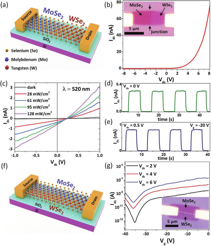
www.advancedsciencenews.com www.afm-journal.de
chemical vapor deposition (CVD)[22–24] is employed for growing The growth substrate was placed next to and downstream
TMD lateral heterostructures by lateral edge epitaxy.[18,20] A two- of the oxide precursors. We used Ar as a carrier gas to trans-
step growth procedure in which regions of different TMDs are port the precursors to the growth substrate. Our growth proce-
grown one after another in subsequent growth experiments is dure has two different heating steps for growing the MoSe2 and
the most common approach for obtaining TMD lateral hetero- WSe2 areas of the lateral heterostructure. The growth substrate
structures.[21–23] However, this method is difficult to scale up together with the metal oxide precursors was initially heated
and the TMD layer grown initially has to be exposed to ambient to a temperature of 730 °C. At this temperature, a flow of H2
conditions for the preparation of the second growth, which may was introduced. This temperature is sufficient for the evapo-
have detrimental effects to the interface. In general, CVD is the ration of molybdenum oxychloride species which reacts with
most viable approach to produce TMDs due to its simplicity as the incoming Se atoms forming the MoSe2 monolayer areas
well as lower growth temperatures in comparison with PVD on the growth substrate. The substrates were kept at this temper-
techniques.[22–24] By employing a one-step CVD approach with ature for 30 min to ensure complete evaporation and removal of
suitable growth conditions, TMD lateral heterostructures can the Mo-containing precursor from the furnace. Next, the flow of
be grown sequentially by lateral edge epitaxy without exposure H2 was stopped and the temperature was increased to 800 °C. At
to ambient conditions.[24] However, such a growth procedure is this temperature, a flow of H2 was reintroduced into the furnace.
challenging due to the possibility of precursor mixing, resulting The samples were kept under this condition for the next 15 min
in alloying, and subsequent poor quality of the p–n junction. for the growth of WSe2. The WSe2 nucleates and grows prefer-
In this communication, we demonstrate a simple one-pot ably at the edges of the MoSe2 crystals by lateral edge epitaxy[18,22]
CVD method of large area MoSe2-WSe2 lateral heterostructures forming the MoSe2-WSe2 lateral heterostructure. In addition,
by subsequent selective evaporation of the metal oxide precur- we tested the growth of WSe2 at 730 °C (with similar conditions
sors by adjusting their precursor partial pressures during the for the MoSe2 growth) and no deposition of isolated WSe2 crys-
growth process using differential heating. We have characterized tals takes place. This experimental observation is supported by
the grown lateral heterostructures by optical microscopy (OM), the thermodynamic assessment of the system (see page 6 and
Raman spectroscopy, atomic force microscopy (AFM), and pho- Figure S2, Supporting Information). At 730 °C, partial pressure
toluminescence (PL) spectroscopy for probing their morpho- of the Mo-containing species is ≈200 times higher than the par-
logical, structural, and optical properties. Furthermore, we have tial pressure of the W-containing species, which indicates that
employed aberration-corrected high-resolution transmission MoO3 precursor can evaporate completely already at 730 °C, (see
electron microscopy (HRTEM) and high-angle annular dark-field Figures S2 and S3, Supporting Information). Moreover, a flow
scanning transmission electron microscopy (HAADF-STEM) of H2 is essential for the growth of both MoSe2 and WSe2 areas,
combined with energy-dispersive X-ray spectroscopy (EDX) to as it facilitates fast reduction of the oxide precursors to maintain
reveal the high-quality interface between the MoSe2 and WSe2 sufficient concentration of transition metal precursors during
areas of the lateral heterostructure. We have then realized atomi- the growth.[28,29] Thus, by controlling vapor pressure of the pre-
cally thin electronic and optoelectronic p–n junction devices, cursors by temperature and H2 flow rates, we could successfully
which can be used as rectifiers and exhibit photovoltaic character- grow large area MoSe2-WSe2 lateral heterostructures.
istics under illumination with light. Furthermore, we have dem- As can be seen from Figure 1b,c and Figure 2, the grown
onstrated that the heterojunction devices can be employed as a MoSe2-WSe2 heterostructures have mostly hexagonal, star-
self-powered photovoltaic photodetector or ambipolar field-effect like, or triangular shape with typical lateral sizes of inner and
transistor. Under suitable biasing conditions, we have observed outer areas of 20–60 µm (see also Figure S4, Supporting Infor-
electroluminescent emission from our devices showing their mation, for additional images and description). To study their
potential applicability as ultrathin light-emitting diodes (LEDs). topography, we characterized the lateral heterostructures with
an AFM using the tapping mode. Thus, Figure 1d,e present the
respective height and phase images of the area highlighted in
2. Results and Discussion Figure 1c with a dashed square. The height profile across the
lateral heterostructure on the SiO2 substrate, corresponding to
We used a modified CVD method which employs a Knudsen the dashed line in Figure 1d, is shown as an inset. The esti-
type effusion cell (Figure S1, Supporting Information) to deliver mated heterostructure height of 0.8 ± 0.3 nm corresponds well
the chalcogen precursors for the growth of the lateral hetero- to the monolayer thickness. A boundary between MoSe2 and
structures.[25] This technique has been shown to produce high- WSe2 areas can be recognized in the phase image (Figure 1e);
quality transition metal disulfide monolayers.[26] A scheme however, as expected for an atomically flat sheet, the height var-
of the CVD setup is presented in Figure 1a. The Se precursor iation is not observed between the areas covered with different
was loaded into the quartz effusion cell (see page 5 Supporting TMDs. A root mean square roughness of the heterostructure
Information) and placed upstream in an inner tube at the low- areas (measured on an area of 5 × 5 µm2) was found to be
temperature zone of the furnace. The temperature of the Se 0.3 ± 0.1 nm, which further confirms its atomic flatness.
precursor was maintained at ≈400 °C during the growth pro- Next, to confirm the structural identity of the MoSe2 and WSe2
cedure. The MoO3 and WO3 precursors were placed on two areas, we performed Raman spectroscopy and microscopy meas-
different silicon substrates inside the inner quartz tube and urements. In Figure 2a,b, we show Raman spectra recorded on
located in the high-temperature zone of the furnace. We have the inner MoSe2 area and the outer WSe2 area of the lateral het-
mixed a certain amount of NaCl to the oxide precursors to pro- erostructure presented in Figure 2a as an inset. The formation
mote faster evaporation of the oxides by forming highly volatile of MoSe2 is confirmed by the A1g peak at 240.5 cm−1 originating
molybdenum oxychloride or tungsten oxychloride species.[27] from the out-of-plane vibrations of the Se atoms and E2g peak at
Adv. Funct. Mater. 2021, 2101086 2101086 (2 of 9) © 2021 The Authors. Advanced Functional Materials published by Wiley-VCH GmbH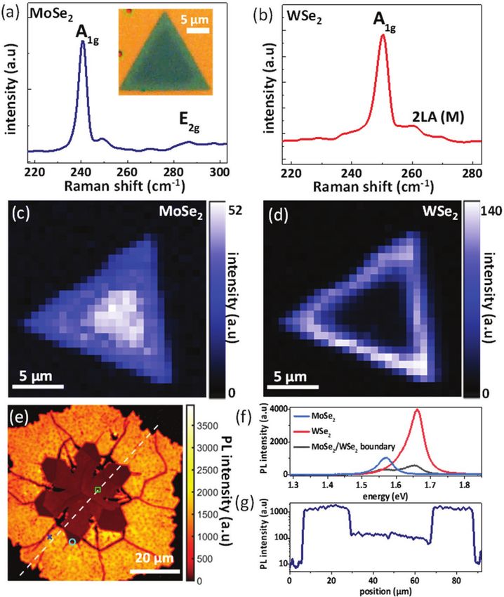
www.advancedsciencenews.com                                                                                                        www.afm-journal.de

Figure 1. One-pot CVD growth of MoSe2-WSe2 lateral heterostructures. a) Schematic diagram of the CVD growth setup. b–c) OM images of MoSe2-
WSe2 lateral heterostructures. False colors are used to enhance contrast between the MoSe2 and WSe2 areas. The area highlighted within the dashed
square in (c) is imaged using an atomic force microscope in the tapping mode. d) AFM height image shows no contrast between the MoSe2 and WSe2
areas. The height profile between the SiO2 substrate and the heterostructure is shown using solid white line (the height profile is extracted from the
dashed white line). The thickness of the lateral heterostructure is estimated as 0.8 ± 0.3 nm which corresponding to a monolayer. Furthermore, there
is no height difference between the MoSe2 and WSe2 areas, whereas they can be clearly recognized in the respective AFM phase image (e).

286 cm−1 originating from the in-plane vibrations of the Mo and              is only detected in the inner area of the heterostructure. Since the
Se atoms.[30] The A1g peak at 250 cm−1 originating from the out-of-          laser beam diameter was ≈1–2 µm, the MoSe2 area appears to be
plane vibrations of the Se atoms confirms the formation of WSe2,             slightly larger than the actual size. A line scan of Raman spectra
Figure 2b.[31,32] The 2LA(M) mode at 260.5 cm−1 originating from             recorded on a bigger lateral heterostructure is provided in Figure
the longitudinal acoustic phonons, which are in-plane collective             S6, Supporting Information. From the intensity map of the A1g
periodic compressions and expansions of atoms in the lattice, is             peak of WSe2 presented in Figure 2d, it is evident that WSe2 is
also present in the WSe2 spectra.[32] A Raman spectrum recorded              only present in the outer area confirming the formation of the
at the border region of the MoSe2 and WSe2 areas is presented                expected lateral heterostructure. Additionally, the chemical iden-
in Figure S5, Supporting Information, showing a superposition                tity of the formed lateral heterostructure was confirmed by X-ray
of the characteristic peaks of both materials. Intensity maps of             photoelectron spectroscopy (XPS) (see Figure S7, Supporting
the A1g Raman modes of MoSe2 and WSe2 mapped on the entire                   Information, for details).
MoSe2-WSe2 heterostructure are presented in Figure 2c,d, respec-                 The optical quality of the grown lateral heterostructures was
tively. As seen from Figure 2c, intensity of the A1g peak of MoSe2           probed by room-temperature PL measurements using a 532 nm

Adv. Funct. Mater. 2021, 2101086         2101086 (3 of 9)                  © 2021 The Authors. Advanced Functional Materials published by Wiley-VCH GmbH

www.advancedsciencenews.com                                                                                                        www.afm-journal.de

Figure 2. Raman spectroscopy and imaging of the MoSe2-WSe2 lateral heterostructures. A laser with λ = 532 nm is used to excite the Raman modes.
a) Raman spectrum recorded on the MoSe2 inner area showing the A1g characteristic peak at 240.5 cm−1. The inset shows an OM image of the MoSe2-WSe2
lateral heterostructure on which the Raman measurements are conducted. b) Raman spectrum recorded on the WSe2 outer area of the heterostructure
showing the A1g peak at 250 cm−1. c–d) Raman intensity map of the MoSe2-WSe2 heterostructure. In (c) the A1g peak of MoSe2 is mapped and in (d)
the A1g peak of WSe2 is mapped. e–g) PL of the WSe2-MoSe2 lateral heterostructure. e) PL-map of the heterostructure, with indicators for the lineout
in (f) and the positions at which PL-spectra have been measured in (g). f) PL-intensity along the lineout displayed in (e). The outer WSe2-section has
an intensity of 1700 ± 170 a.u., whereas the intensity of the inner MoSe2-area has a brightness of 126 ± 20 a.u. g) Typical PL-spectra at the positions
marked in (e) WSe2 with a mean energy of 1.655 ± 0.03 eV and an FWHM of 0.16 ± 0.01 eV (red). MoSe2 with a mean energy of 1.56 ± 0.02 eV and an
FWHM of 0.06 ± 0.005 eV (blue). On the border with clear contributions by both materials (dark).

laser for the excitation. Figure 2e shows a PL spatial map of a              alloys on the respective length scale. Figure 2g presents the
MoSe2-WSe2 heterostructure. It can be seen that the inner part               characteristic PL spectra acquired at the WSe2 and the MoSe2
(MoSe2) and the outer part (WSe2) of the heterostructure show                areas as well as at the boundary region. For the MoSe2 we
different PL intensities. As can be seen from the PL line profile            measure an average peak wavelength of 790 nm (1.568 eV) with
(extracted from the dashed line in Figure 2e), the PL intensity              an FWHM bandwidth of 60 meV. For the WSe2 an average peak
from the WSe2 is on average about 10 times higher than from                  wavelength of 748 nm (1.656 eV) with an FWHM bandwidth of
the MoSe2 (see Figure 2f); it is homogeneous for each mate-                  68 meV was detected. These values are consistent with the data
rial within ≈15%. Moreover, within the lateral resolution of the             reported for high-quality pristine monolayer crystals fabricated
employed optical microscope (≈1 µm) a sharp border between                   by CVD.[29,33] We, therefore, conclude that the fabricated hetero-
two materials is observed, which excludes the formation of                   structure consists of well-separated areas, where these areas are

Adv. Funct. Mater. 2021, 2101086         2101086 (4 of 9)                  © 2021 The Authors. Advanced Functional Materials published by Wiley-VCH GmbH
www.advancedsciencenews.com                                                                                                       www.afm-journal.de

Figure 3. HAADF-STEM characterization of the MoSe2-WSe2 heterostructure. a) shows a 120 kV HAADF-STEM overview image of the lateral hetero-
structure on a holey-carbon TEM grid (the holes in the TEM grid appear black in the image and the greyish contrast originates from the flake of the
lateral WSe2 and MoSe2 heterostructure, please notice its atomic-number-related contrast difference: deeper grey: MoSe2, lighter grey: WSe2). The
corresponding EDX maps in (b) and (c) allow the identification of the element distribution: b) W (green), Mo (blue), and c) Se (orange).

of the same properties as the individual materials when they are           exhibits a dark current of 135 pA at a source-drain bias (Vds) of
grown separately. The PL observed for WSe2 is stronger than                1 V. When irradiating the device, a clear photovoltaic effect can
that for MoSe2. This difference is typical for our growth process          be observed. For instance, when irradiating with an intensity
and is likewise observed for individual material samples; hence            of 61 ± 5 mW cm−2 the device shows an open-circuit voltage
we argue that the quality of neither material is degraded in the           (VOC) of 0.24 V and a short-circuit current (ISC) of 354 pA. The
lateral heterostructure growth process.                                    fill factor (FF) of the device is calculated as 0.27. The power con-
   To further characterize the lateral MoSe2-WSe2 heterostruc-             version efficiency (PCE), that is, the ratio of output electrical
ture interface, we performed HAADF-STEM combined with                      power to the incident light power can be calculated using the
EDX as well as chromatic (Cc) and spherical (Cs) aberration-                                    I × VOC × FF
                                                                           equation, PCE = SC                  , where Pincident is the incident
corrected HRTEM. In Figure 3a, we show an overview HAADF-                                            Pincident
STEM image of the lateral heterostructure on a holey carbon                laser power. The PCE is calculated as 0.12%, which is similar
TEM grid and Figure 3b,c demonstrate the corresponding                     to the reported values on similar TMD-based junctions.[11,23,34]
Mo/W- and Se-EDX maps, respectively. The HRTEM unambig-                    We have fabricated and characterized five p–n junction hetero-
uously confirms the formation of a monolayer heterostructure               structure devices and all of the devices show similar behavior.
(see Figure S8, Supporting Information), whereas the formation             We estimated the photoresponse also theoretically (see
of large-sized MoSe2 and WSe2 areas, as well as a very straight            Figure S9, Supporting Information) using density functional
boundary, are clearly revealed from HAADF-STEM (see red                    theory (DFT) calculations by adding the electron–photon inter-
arrows in Figure 3a). Note that the edge of the WSe2 area pos-             action into the device Hamiltonian employing the first-order
sesses a saw-toothed shape. As more electrons are scattered to             perturbation theory,[35] see page 8 Supporting Information.
higher angles from the heavier W in comparison to lighter Mo,              The onset of the photocurrent was found at a photon energy of
the WSe2 area appears brighter than that of MoSe2. From the                2.35 eV, just below the 520 nm of the laser light applied experi-
contrast analysis in Figure 3a and the respective EDX maps                 mentally. However, the calculations also show that the photo-
in Figure 3b,c we conclude that Se is homogeneously distrib-               current is sensitive to the doping level of the devices and to
uted on the whole heterostructure area, whereas Mo and W are               the defect concentration. For a doped junction, the onset of the
present in the inner and outer regions, respectively. The EDX              photocurrent was found at a lower photon energy of 2.15 eV and
spectra were acquired over such long exposure time, the signal-            the photocurrent is larger compared to the undoped junction.
to-noise ratio of the monolayer is small explaining very faint             Hence, this result can be considered as a qualitative proof of the
signals outside the flake originating from noise only.                     applicability of the heterostructures devices in a photovoltaic cell.
   Monolayer lateral heterostructures of n-type MoSe2 and p-type               In Figure 4d and Figure 4e we show the optical response of the
WSe2 enable the realization of atomically thin electronic and              device with alternating light pulses (λ = 520 nm, 61 ± 5 mW/cm2).
optoelectronic p–n junction devices. Next, we fabricated devices           The data in Figure 4d is acquired without any applied Vds dem-
with the lateral heterostructures in two different configurations          onstrating a self-powered photovoltaic photodetector. The rise
as shown schematically in Figure 4a,f. In the first type of device,        (τrise) and fall (τfall) time constants of photocurrent can be esti-
the p-type WSe2 and n-type MoSe2 areas are connected in series             mated by fitting the curves using a single exponential growth
with source and drain electrodes defined on each material as               and decay function as shown in Figure S11a, Supporting Infor-
shown in Figure 4a. A current–voltage (I–V) characteristic of              mation. The τrise and τfall are estimated as 0.16 ± 0.01 s and
such a p–n junction diode device is shown in Figure 4b (Inset              0.15 ± 0.01 s respectively when the photodetector is operated
of 4b shows OM image). The rectification behavior of the diode             without any applied bias. The on/off ratio of the photodetector
can be observed from the I–V characteristics (i.e., the diode              is in the order of 104 at Vds = 0 V without the application of a
allowed electrical conduction only when it is operated in for-             gate voltage. The data in Figure 4e is acquired with an applied
ward bias). Next, we tested the photoresponse of the device by             bias, Vds = +0.5 V and applied gate voltage, Vg = −20 V. We
irradiating it using a 520 nm laser. In Figure 4c, the I–V charac-         applied a Vg = − 20 V to adjust the off current to a minimum.
teristics of a p–n junction device under dark and under illumina-          In this case, the on/off ratio of the device is estimated in the
tion with varying intensities of the laser are shown. The device           order of 102 and the τrise and τfall are estimated as 0.17 ± 0.01 s

Adv. Funct. Mater. 2021, 2101086        2101086 (5 of 9)                  © 2021 The Authors. Advanced Functional Materials published by Wiley-VCH GmbH
www.advancedsciencenews.com www.afm-journal.de
Figure 4. Electronic and optoelectronic characterization of p–n junction devices fabricated using the MoSe2-WSe2 lateral heterojunctions. a) Scheme
of the p–n junction device. b) The I–V curve of MoSe2-WSe2 lateral heterostructure p–n junction device shows strong rectification behavior. The inset
shows an OM image of the device. The p–n junction device channels are lithographically defined to enable the charge transport only in the precise
device channel contrary to previously published reports.[15,18,21] c) The I–V characteristics of the p–n junction device at dark and under illumination
(λ = 520 nm) with varying laser intensities. The photovoltaic response of the p–n junction device can be clearly observed. d–e) Light pulses are applied
to the device using a laser with λ = 520 nm at an intensity of 61 mW cm−2 and the optical response is measured as a function of time. d) The device
shows photovoltaic response to the light without applying a source-drain bias (photovoltaic photodetector). Even a higher photoresponse is observed
when the device is measured by applying a Vds = +0.5 V and a Vg = −20 V (e). The analysis of the rise and fall time constants of photocurrent is
shown in Figure S9, Supporting Information. f–g) Characterization of ambipolar field-effect transistors fabricated using MoSe2-WSe2 parallel channels.
f) Schematic of the ambipolar field-effect transistor device. g) Transfer characteristics recorded at different source-drain voltages (Vds) show ambipolar
transport behavior. An OM image of the device is shown in the inset. The dashed white line represents the boundary between MoSe2 and WSe2.
and 0.15 ± 0.01 s respectively (Figure S11b, Supporting Informa- estimated as 110 mA W−1. In Figure S12, Supporting Infor-
tion). We estimated the responsivity of the photodetector, that mation, we show the tunability of responsivity with respect
is, the photocurrent generated per unit power of the incident to Vds (at Vg = 0 V) when irradiating with an intensity of
I ph − I dk 28 ± 5 mW cm−2 extracted from the data presented in Figure 4c.
light using the equation R λ = , where Rλ is the respon-
Pincident The external quantum efficiency (EQE) of the device, that is,
sivity, Iph is the photocurrent, and Idk is the dark current. In the the ratio of number of photo-induced carriers to the number
photovoltaic photodetector operation mode, the responsivity of incident photons of the device can be estimated using the
hc
is estimated as 18 mA W−1 at an incident laser power of 28 ± equation, η = Rλ × × 100%, where h is the Planck’s constant, c
λe
5 mW cm−2. With an applied Vds = +1 V, the responsivity is is the speed of light, λ is the wavelength of light used, and e is
Adv. Funct. Mater. 2021, 2101086 2101086 (6 of 9) © 2021 The Authors. Advanced Functional Materials published by Wiley-VCH GmbHwww.advancedsciencenews.com www.afm-journal.de
the electron charge. In the photovoltaic photodetector operation as expected. In such a device configuration, the p-channel
mode (Vds = 0), the EQE is calculated as 4.3%. When applying (WSe2) becomes conductive towards negative Vg and the
Vds = +1 V the EQE is 23.4%. The detectivity (d*) of a photo- MoSe2 n-channel becomes conductive towards more positive
S Vg. It can be seen that the minimum conductivity points of
detector can be calculated using the equation d ∗ = R λ ; the transfer curves shifted towards the negative gate voltages
2eI dk
possibly due to substantial n-doping induced by the SiO2 sub-
where S is the effective area of the photodetector. The detectivi- strate as well as the transfer process.[38]
ties are calculated as 1 × 10⁹ Jones and 6 × 10⁸ Jones at Vds = 0 The serial p–n junction devices were also tested for their
and Vds = +1 V, respectively. The figures of merit of the hetero- suitability as electroluminescent photon emitters. The devices
structure photodetector are comparable to previously reported were operated under forward bias voltage with both current
photodetectors fabricated using TMD-based materials and junc- and light emission measured in the process. The light emis-
tions.[36] When operating at the photovoltaic mode, the photo- sion was measured using a high-resolution camera through
detector shows a high on/off ratio in the order of 104, which a microscopic objective. The camera images displayed in
is higher than most of the previously reported TMD-based Figure 5a,b clearly show that light is detected in a diffraction-
photodetectors. Such self-powered optoelectronic devices are limited spot on the position of the heterostructure junction
desirable building blocks for energy-efficient electronic equip- only if voltage is supplied. A series of images with varying
ment since no additional energy supply is required. Addition- supply voltages were recorded together with the device current.
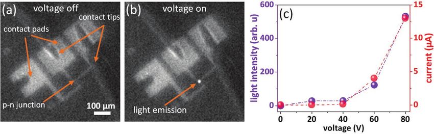
ally, we performed electrical and optoelectronic measurements The results are displayed in Figure 5c. Light emission onset
on devices made of individually grown MoSe2 and WSe2 mon- can be observed at a voltage of roughly 50 to 60 V, with typical
olayers (see pages 9-10 Supporting Information for details and electrical currents in the microampere range. Light emission
Figures S13–S16, Supporting Information for the OM, AFM, could be observed reproducibly over hours for voltages up to
Raman, and XPS characterization of individually grown mon- 100 V. Considering the number of detected photons and the
olayers of MoSe2 and WSe2). These devices do not show any detection efficiency of the setup, we estimate the internal
rectification/photovoltaic effect, which demonstrates that quantum efficiency of the emission process to be in the range
the presence of the p–n junctions due to the 1D MoSe2-WSe2 of 10−7. High operation voltages are assumed to originate from
boundary is responsible for the rectification, photovoltaic, the contacts operating in the Schottky mode as well as due to
and self-power photodetector effects (see pages 9-10 and high channel resistance.
Figures S17–S19, Supporting Information).
The second type of devices was fabricated in such a way that
the MoSe2 and WSe2 areas were connected in parallel to the 3. Conclusion
source-drain electrodes as shown schematically in Figure 4f.
The junction between the p and n region is in the middle per- In summary, we have demonstrated a simple and reproduc-
pendicular to the electrodes. Such devices with parallel p-type ible method to synthesize large-area monolayer lateral het-
(WSe2) and n-type (MoSe2) channels are expected to function erostructures of MoSe2 and WSe2 by controlling the precursor
as ambipolar field-effect transistors.[37] The ambipolar transis- evaporation in a scalable one-pot CVD process. The grown
tors are promising building blocks for applications including heterostructures were characterized using optical and AFM,
lighting, display, memory, logic, and neuromorphic com- Raman, and XPS as well as PL measurements to reveal their
puting devices.[35] An OM image of an ambipolar transistor morphological, structural, chemical, and optical quality. Using
is shown in the inset of Figure 4g. We performed field-effect TEM, we have confirmed the high quality of 1D boundary
transport measurements on such devices and transfer char- between the MoSe2 and WSe2 in their lateral heterostructure.
acteristics, that is, the enhancement of drain current with We fabricated p–n junction devices using the synthesized het-
applied Vg at different applied Vds, are shown in Figure 4g. erostructures and demonstrated their applicability as rectifiers,
The transfer characteristics demonstrate ambipolar transport photovoltaic cells (solar cells), self-powered photodetectors,
Figure 5. LED type emission from the monolayer MoSe2-WSe2 lateral heterostructure p–n junction device. a) Microscope image of the heterostructure
in voltage “off” state and with and applied voltage of 60 V (“on”) via the square contact pads. Light emission is seen as a bright spot of diffraction-
limited size appearing at the heterostructure location. b) Light intensity and current through the junction as a function of input voltage (the dashed
lines are provided as a guide to the eye).
Adv. Funct. Mater. 2021, 2101086 2101086 (7 of 9) © 2021 The Authors. Advanced Functional Materials published by Wiley-VCH GmbHwww.advancedsciencenews.com www.afm-journal.de
and light-emitting devices. Furthermore, we demonstrated Keywords
the possibility of ambipolar field-effect transistors using later-
lateral heterostructures, light-emitting diode, p–n junction, transition
ally connected parallel MoSe2-WSe2 channels. We expect that
metal dichalcogenides monolayers, 2D devices
high-quality 1D p–n junctions are of high interest for solid-state
physics in general, as they pose an opportunity to study the Received: February 22, 2021
impact of the dimensionality on the dynamics of excitations in Revised: March 23, 2021
solid-state boundaries. We also anticipate that our findings will Published online:
facilitate the ongoing search for sub-nanometer, non-silicon
electronic, optoelectronic, and photovoltaic devices.
[1] a) S. Manzeli, D. Ovchinnikov, D. Pasquier, O. V. Yazyev, A. Kis,
Nat. Rev. Mater. 2017, 2, 17033; b) Z. Cai, B. Liu, X. Zou,
Supporting Information H.-M. Cheng, Chem. Rev. 2018, 118, 6091.
Supporting Information is available from the Wiley Online Library or [2] W. Choi, N. Choudhary, G. H. Han, J. Park, D. Akinwande, Y. H. Lee,
from the author. Mater. Today 2017, 20, 116.
[3] N. Choudhary, M. A. Islam, J. H. Kim, T.-J. Ko, A. Schropp,
L. Hurtado, D. Weitzman, L. Zhai, Y. Jung, Nano Today 2018,
19, 16.
Acknowledgements [4] H. Zhou, C. Wang, J. C. Shaw, R. Cheng, Y. Chen, X. Huang, Y. Liu,
The authors acknowledge financial support of the Thüringer MWWDG via N. O. Weiss, Z. Lin, Y. Huang, X. Duan, Nano Lett. 2015, 15, 709.
the “ProExzellenz 2014–2019” programme under the grants “ACPExplore2016” [5] A. Kuc, T. Heine, A. Kis, MRS Bull. 2015, 40, 577.
and “ACPExplore2018” as well as the Deutsche Forschungsgemeinschaft [6] R. Frisenda, A. J. Molina-Mendoza, T. Mueller, A. Castellanos-Gomez,
(DFG) through a research infrastructure grant INST 275/257-1 FUGG and H. S. J. van der Zant, Chem. Soc. Rev. 2018, 47, 3339.
CRC 1375 NOA (Project B2 and Project B3). This project has also received [7] S. Lei, X. Wang, B. Li, J. Kang, Y. He, A. George, L. Ge, Y. Gong,
funding from the joint European Union’s Horizon 2020 and DFG research P. Dong, Z. Jin, G. Brunetto, W. Chen, Z.-T. Lin, R. Baines,
and innovation programme FLAG-ERA under grant TU149/9-1. T.L. and D. S. Galvão, J. Lou, E. Barrera, K. Banerjee, R. Vajtai, P. Ajayan,
U.K. acknowledge funding from the DFG and the Ministry of Science, Nat. Nanotechnol. 2016, 11, 465.
Research and the Arts (MWK) of the federal state of Baden-Württemberg [8] Y. Gong, J. Lin, X. Wang, G. Shi, S. Lei, Z. Lin, X. Zou, G. Ye, R. Vajtai,
(Germany) in the frame of the SALVE project (www.salve-project.de), as well B. I. Yakobson, H. Terrones, M. Terrones, B. K. Tay, J. Lou, S. T. Pantelides,
as the European Union in the frame of the Graphene Flagship. F.E. and T.V., Z. Liu, W. Zhou, P. M. Ajayan, Nat. Mater. 2014, 13, 1135.
acknowledge support by the Federal Ministry of Education and Science of [9] a) L. Liu, N. Xu, Y. Zhang, P. Zhao, H. Chen, S. Deng, Adv. Funct.
Germany under Grant ID 13XP5053A. F.E. was supported by the Max Planck Mater. 2019, 29, 1807893; b) C.-Y. Lin, X. Zhu, S.-H. Tsai, S.-P. Tsai,
School of Photonics. E.N. and Q.G.N. are supported by the European S. Lei, Y. Shi, L.-J. Li, S.-J. Huang, W.-F. Wu, W.-K. Yeh, Y.-K. Su,
Union, the European Social Funds and the Federal State of Thuringia under K. L. Wang, Y.-W. Lan, ACS Nano 2017, 11, 11015.
Grant ID 2018FGR00088. The authors thank Stephanie Höppener and
[10] W. Wu, Q. Zhang, X. Zhou, L. Li, J. Su, F. Wang, T. Zhai,
Ulrich S. Schubert for enabling the Raman spectroscopy and microscopy
Nano Energy 2018, 51, 45.
studies at the Jena Center for Soft Matter (JCSM).
[11] C.-H. Lee, G.-H. Lee, A. M. van der Zande, W. Chen, Y. Li, M. Han,
Open access funding enabled and organized by Projekt DEAL.
X. Cui, G. Arefe, C. Nuckolls, T. F. Heinz, J. Guo, J. Hone, P. Kim,
Nat. Nanotechnol. 2014, 9, 676.
[12] M.-L. Tsai, M.-Y. Li, J. R. D. Retamal, K.-T. Lam, Y.-C. Lin, K. Suenaga,
Conflict of Interest L.-J. Chen, G. Liang, L.-J. Li, J.-H. He, Adv. Mater. 2017, 29, 1701168.
[13] A. Pospischil, M. M. Furchi, T. Mueller, Nat. Nanotechnol. 2014, 9,
The authors declare no conflict of interest.
257.
[14] T. Vogl, K. Sripathy, A. Sharma, P. Reddy, J. Sullivan, J. R. Machacek,
L. Zhang, F. Karouta, B. C. Buchler, M. W. Doherty, Y. Lu, P. K. Lam,
Author Contributions Nat. Commun. 2019, 10, 1202.
[15] M.-Y. Li, J. Pu, J.-K. Huang, Y. Miyauchi, K. Matsuda, T. Takenobu,
E.N. and Z.G. contributed equally to this work. A.G. and A.T. conceived
L.-J. Li, Adv. Funct. Mater. 2018, 28, 1706860.
the research and designed the experiments. Z.G., E.N., and A.G.
[16] C. Palacios-Berraquero, M. Barbone, D. M. Kara, X. Chen,
synthesized the lateral heterostructures by CVD and performed basic
material characterizations. Z.G. performed the thermodynamic analysis I. Goykhman, D. Yoon, A. K. Ott, J. Beitner, K. Watanabe,
to interpret the growth process. C.N. performed Raman spectroscopy T. Taniguchi, A. C. Ferrari, M. Atatüre, Nat. Commun. 2016, 7,
and XPS. T.B. and F.E. performed the PL spectroscopy and analysis with 12978.
the guidance of I.S. T.L. and U.K. performed the HRTEM and HAADF- [17] a) R. Frisenda, E. Navarro-Moratalla, P. Gant, D. Pérez De Lara,
STEM analysis. U.H. fabricated the electrical devices. E.N., A.G., and P. Jarillo-Herrero, R. V. Gorbachev, A. Castellanos-Gomez, Chem.
D.K.performed the electrical/optoelectronic measurements and data Soc. Rev. 2018, 47, 53; b) H. Xue, Y. Wang, Y. Dai, W. Kim, H. Jussila,
analysis. G.Q.N., F.E., and E.N. performed the electroluminescence M. Qi, J. Susoma, Z. Ren, Q. Dai, J. Zhao, K. Halonen, H. Lipsanen,
measurements. T.V. performed the DFT calculations and interpretation. X. Wang, X. Gan, Z. Sun, Adv. Funct. Mater. 2018, 28, 1804388;
A.G., F.E., and A.T. wrote the manuscript with input from all authors. c) W. Gao, F. Zhang, Z. Zheng, J. Li, ACS Appl. Mater. Interfaces
2019, 11, 19277.
[18] P. K. Sahoo, S. Memaran, Y. Xin, L. Balicas, H. R. Gutiérrez, Nature
2018, 553, 63.
Data Availability Statement [19] C. Huang, S. Wu, A. M. Sanchez, J. J. P. Peters, R. Beanland,
The data that support the findings of this study are available from the J. S. Ross, P. Rivera, W. Yao, D. H. Cobden, X. Xu, Nat. Mater. 2014,
corresponding author upon reasonable request. 13, 1096.
Adv. Funct. Mater. 2021, 2101086 2101086 (8 of 9) © 2021 The Authors. Advanced Functional Materials published by Wiley-VCH GmbHwww.advancedsciencenews.com www.afm-journal.de
[20] F. Ullah, Y. Sim, C. T. Le, M.-J. Seong, J. I. Jang, S. H. Rhim, [30] J. Xia, X. Huang, L.-Z. Liu, M. Wang, L. Wang, B. Huang, D.-D. Zhu,
B. C. Tran Khac, K.-H. Chung, K. Park, Y. Lee, K. Kim, H. Y. Jeong, J.-J. Li, C.-Z. Gu, X.-M. Meng, Nanoscale 2014, 6, 8949.
Y. S. Kim, ACS Nano 2017, 11, 8822. [31] a) P. Tonndorf, R. Schmidt, P. Bottger, X. Zhang, J. Borner,
[21] K. Chen, X. Wan, J. Wen, W. Xie, Z. Kang, X. Zeng, H. Chen, J.-B. Xu, A. Liebig, M. Albrecht, C. Kloc, O. Gordan, D. R. Zahn,
ACS Nano 2015, 9, 9868. S. Michaelis de Vasconcellos, R. Bratschitsch, Opt. Express 2013,
[22] Y. Zhang, L. Yin, J. Chu, T. A. Shifa, J. Xia, F. Wang, Y. Wen, X. Zhan, 21, 4908; b) X. Zhang, X.-F. Qiao, W. Shi, J.-B. Wu, D.-S. Jiang,
Z. Wang, J. He, Adv. Mater. 2018, 30, 1803665. P.-H. Tan, Chem. Soc. Rev. 2015, 44, 2757.
[23] M.-Y. Li, Y. Shi, C.-C. Cheng, L.-S. Lu, Y.-C. Lin, H.-L. Tang, [32] M. Yang, X. Cheng, Y. Li, Y. Ren, M. Liu, Z. Qi, Appl. Phys. Lett. 2017,
M.-L. Tsai, C.-W. Chu, K.-H. Wei, J.-H. He, W.-H. Chang, K. Suenaga, 110, 093108.
L.-J. Li, Science 2015, 349, 524. [33] X. Wang, Y. Gong, G. Shi, W. L. Chow, K. Keyshar, G. Ye, R. Vajtai, J. Lou,
[24] J. Lee, S. Pak, Y.-W. Lee, Y. Park, A. R. Jang, J. Hong, Y. Cho, B. Hou, Z. Liu, E. Ringe, B. K. Tay, P. M. Ajayan, ACS Nano 2014, 8, 5125.
S. Lee, H. Y. Jeong, H. S. Shin, S. M. Morris, S. Cha, J. I. Sohn, [34] a) F. Wang, Z. Wang, K. Xu, F. Wang, Q. Wang, Y. Huang,
J. M. Kim, ACS Nano 2019, 13, 13047. L. Yin, J. He, Nano Lett. 2015, 15, 7558; b) S. Jia, Z. Jin, J. Zhang,
[25] A. George, C. Neumann, D. Kaiser, R. Mupparapu, T. Lehnert, J. Yuan, W. Chen, W. Feng, P. Hu, P. M. Ajayan, J. Lou, Small
U. Hübner, Z. Tang, A. Winter, U. Kaiser, I. Staude, A. Turchanin, 2020, 16, 2002263; c) M. M. Furchi, A. Pospischil, F. Libisch,
J. Phys.: Mater. 2019, 2, 016001. J. Burgdörfer, T. Mueller, Nano Lett. 2014, 14, 4785; d) Y. Deng,
[26] S. Shree, A. George, T. Lehnert, C. Neumann, M. Benelajla, Z. Luo, N. J. Conrad, H. Liu, Y. Gong, S. Najmaei, P. M. Ajayan,
C. Robert, X. Marie, K. Watanabe, T. Taniguchi, U. Kaiser, J. Lou, X. Xu, P. D. Ye, ACS Nano 2014, 8, 8292; e) N. Flöry, A. Jain,
B. Urbaszek, A. Turchanin, 2D Mater. 2019, 7, 015011. P. Bharadwaj, M. Parzefall, T. Taniguchi, K. Watanabe, L. Novotny,
[27] S. Li, S. Wang, D.-M. Tang, W. Zhao, H. Xu, L. Chu, Y. Bando, Appl. Phys. Lett. 2015, 107, 123106.
D. Golberg, G. Eda, Appl. Mater. Today 2015, 1, 60. [35] M. Palsgaard, T. Markussen, T. Gunst, M. Brandbyge, K. Stokbro,
[28] a) B. Liu, M. Fathi, L. Chen, A. Abbas, Y. Ma, C. Zhou, ACS Phys. Rev. Appl. 2018, 10, 014026.
Nano 2015, 9, 6119; b) H. Wang, D. Zhu, F. Jiang, P. Zhao, [36] a) J. Yao, G. Yang, Nanoscale 2020, 12, 454; b) M. Long, P. Wang,
H. Wang, Z. Zhang, X. Chen, C. Jin, Nanotechnology 2018, 29, H. Fang, W. Hu, Adv. Funct. Mater. 2019, 29, 1803807.
314001. [37] Y. Ren, X. Yang, L. Zhou, J.-Y. Mao, S.-T. Han, Y. Zhou, Adv. Funct.
[29] J.-K. Huang, J. Pu, C.-L. Hsu, M.-H. Chiu, Z.-Y. Juang, Mater. 2019, 29, 1902105.
Y.-H. Chang, W.-H. Chang, Y. Iwasa, T. Takenobu, L.-J. Li, ACS Nano [38] M. Amani, M. L. Chin, A. L. Mazzoni, R. A. Burke, S. Najmaei,
2014, 8, 923. P. M. Ajayan, J. Lou, M. Dubey, Appl. Phys. Lett. 2014, 104, 203506.
Adv. Funct. Mater. 2021, 2101086 2101086 (9 of 9) © 2021 The Authors. Advanced Functional Materials published by Wiley-VCH GmbHYou can also read