A Technology-Computer-Aided-Design-Based Reliability Prediction Model for DRAM Storage Capacitors - MDPI
←
→
Page content transcription
If your browser does not render page correctly, please read the page content below
micromachines

Article
A Technology-Computer-Aided-Design-Based
Reliability Prediction Model for DRAM
Storage Capacitors
Woo Young Choi 1, * , Gyuhan Yoon 1 , Woo Young Chung 2 , Younghoon Cho 2 , Seongun Shin 1
and Kwang Ho Ahn 2
 1   Department of Electronics Engineering, Sogang University, Seoul 04107, Korea; ghyoon@sogang.ac.kr (G.Y.);
     sapienthia@daum.net (S.S.)
 2   Department of DRAM Sensing & Advanced Analysis, SK Hynix, Icheon 17336, Korea;
     wooyoung.chung@sk.com (W.Y.C.); younghoon1.cho@sk.com (Y.C.); kwangho.ahn@sk.com (K.H.A.)
 *   Correspondence: wchoi@sogang.ac.kr; Tel.: +82-2-715-8467

 Received: 12 March 2019; Accepted: 15 April 2019; Published: 17 April 2019

 Abstract: A full three-dimensional technology-computer-aided-design-based reliability prediction
 model was proposed for dynamic random-access memory (DRAM) storage capacitors. The model
 can be used to predict the time-dependent dielectric breakdown as well as leakage current of a
 state-of-the-art DRAM storage capacitor with a complex three-dimensional structure.

 Keywords: dynamic random-access memory storage capacitor; technology-computer-aided design;
 reliability; leakage current; time-dependent dielectric breakdown

1. Introduction
     Dynamic random-access memory (DRAM) cells are continuously scaled down to improve the
chip density [1]. The cell-size reduction decreases the storage capacitance (Cs ), which is crucial for the
data retention time and read sensing margin [2]. Therefore, cell-size reduction while maintaining Cs is
one of the most important technical issues in DRAM cell design. Two approaches have been employed
to overcome this obstacle: increasing the surface area (A) and increasing the dielectric constant (k)
of the storage capacitor. For the first approach, storage capacitors are converted from planar into
three-dimensional (3D) structures to maximize their aspect ratios [3]. Regarding the second approach,
various types of high-k materials are introduced such as ZrO2 [4], TiO2 [5], and SrTiO [6], which tends
to deteriorate the defect density and bandgap energy [7]. This implies that state-of-the-art DRAM
storage capacitors suffer from reliability issues such as leakage current and time-dependent dielectric
breakdown (TDDB) [8]. Therefore, it is required to predict the electrical reliabilities of DRAM storage
capacitors with complex 3D structures. Several pioneering studies have been carried out to model
the leakage currents [9] and TDDB behaviors [10] of high-k dielectric films based on a kinetic Monte
Carlo (kMC) method; however, the extension to the complex 3D structure is insufficient owing to the
very large computational time [11]. In this manuscript, a full 3D technology-computer-aided-design
(TCAD)-based reliability prediction model for DRAM storage capacitors is proposed. TCAD provides
a faster calculation process than that based on the kMC method and structural changes can also be
easily implemented. The proposed model emulates the leakage current and TDDB behavior based on
any commercial TCAD simulator as long as it provides 3D structure generation, an electron and hole
continuity equation solver, a Poisson equation solver, and physical models including trap-assisted
charge transports [12]. Using this model, the percolation simulation can be applied.

Micromachines 2019, 10, 256; doi:10.3390/mi10040256                       www.mdpi.com/journal/micromachines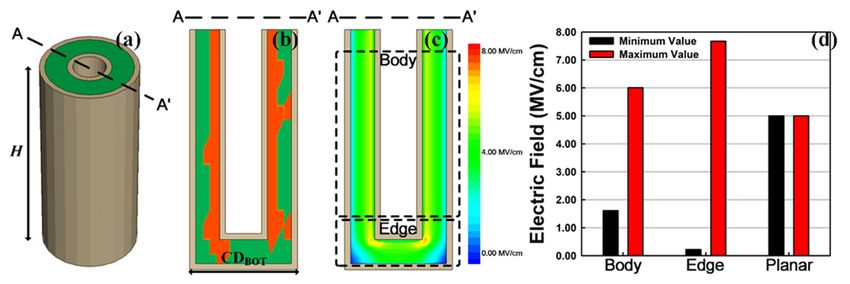
Micromachines 2019, 10, 256                                                                                            2 of 9

2. Methodology
     In this section, the proposed reliability prediction model is explained. The leakage current of
a planar DRAM storage capacitor is simulated using the possible leakage current mechanisms of
metal/insulator/metal (MIM) structures (Figure 1a): (i) thermionic emission, (ii) Fowler–Nordheim
tunneling, (iii) Poole–Frenkel emission (PFE), (iv) trap-assisted tunneling (TAT), (v) trap-to-trap
tunneling, and (vi) direct tunneling. Figure 1b shows the structure of the simulated storage capacitor,
which has a TiN/ZrO2 /TiN stack.
     The leakage currents of ZrO2 -based storage capacitors are affected mainly by PFE and TAT owing
to the high defect density of ZrO2 [13,14]. In addition to the PFE and TAT, the proposed model solved
the electron and hole continuity equations coupled with the Poisson equation:

                                          ∇·(ε∇φ) = −q(p − n + ND − NA ) − ρtrap                                         (1)

                                                   →                               ∂n
                                                ∇· J n = q(Rnet,n − Gnet,n ) + q                                         (2)
                                                                                   ∂t
                                         →                         ∂p
                                    − ∇· J p = q Rnet,p − Gnet,p + q                                  (3)
                                                                     ∂t
where ε is the electrical permittivity, q is the elementary electronic charge, ND is the concentration of
ionized donors, NA is the concentration of ionized acceptors, ρtrap is the charge density contributed
by traps, Rnet,n and Rnet,p are the electron and hole net recombination rates, Gnet,n and Gnet,p are the
                                                     →                                       →
electron and hole net generation rates, J n is the electron current density, J p is the hole current density,
and n and p are the electron and hole densities, respectively. The trap-assisted charge transport was
calculated using the Shockley–Read–Hall (SRH) recombination rate:

                                                             NTRAP cn cp np − n2i
                              Rnet =                                                                                  (4)
                                                     ni
                                                            E                 ni
                                                                                         −E
                                          cn n +     gn   exp kTRAP
                                                                 T     + c p  p + gp exp    TRAP
                                                                                           k T
                                                                 B                           B

where NTRAP is the trap density, ETRAP is the energy of the trap, cn and cp are the electron and hole
capture rates, and gn and gp are the electron and hole degeneracy factors, respectively. All of the used
tunneling models, such as the elastic/inelastic TAT and trap-to-trap tunneling, are nonlocal models.
Only the PFE model was used as a local model and considered to increase the emission rate of electrons
injected through tunneling. The electron capture rate for the phonon-assisted (inelastic) transition from
the conduction band is [15]
                               q
                                   mt m30 k3 Tn3 gc
                                                               α(S−l)2

                                                                                                           ∆E
                                                                                      n                            o
              cninelastic =         } χ
                                      3 √           V TRAP Sω     S     +  1  − α  exp  −S(2 fB   + 1) +   2kT   +χ
                                                                             2                                           (5)
                                                          E −E (0) |Ψ(z0 )|
                                                l
                                      × l+zχ F1/2 F,nkTnC
                                                                      |Ψ(0)|2

where V TRAP is the interaction volume of the trap, S is the Huang–Rhys factor, }ω is the energy of
the phonon involved in the transition, α is a dimensionless parameter, l is the number p     of phonons
emitted
      √  in the  transition, f B is the Bose–Einstein occupation of the phonon state, z = 2S   fB ( fB + 1 ) ,
χ = l + z , ∆E is the dissipated energy, EF,n is the Fermi energy, Tn is the electron temperature,
        2     2

mt is the relative tunneling mass, and gc is the prefactor for the Richardson constant at the interface or
contact. The electron capture rate for the elastic transition from the conduction band is [16]
                                           √
                                               8mt m3/2 gc
                          cnelastic   =             0
                                                 }4 π
                                                       VTRAP [EC (z0 ) − ETRAP ]2 Θ[ETRAP
                                                         p
                                                                              E −E

                                                                                         |Ψ(z0 )|2                       (6)
                                                 −EC (0)] ETRAP − EC (0) f F,n kTnTRAP
                                                                                          | Ψ ( 0 ) |2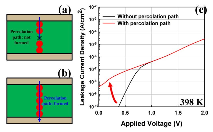
Micromachines 2019, 10, 256 3 of 9
where f (x) = 1/(1 + exp(−x)). The electron capture rate for the trap-to-trap tunneling is [17,18]
" √ √
}WT π 2rj,i 2mt m0 WT
W −W
cntrap−to−trap,i
P OPT T
= Cf 2
exp − 2kT
√ exp − }
j,i mt m0 rj,i Q0 kT
j j
(7)
EiTRAP −ETRAP + EiTRAP −ETRAP
× exp−
2kT fj
where transitions occur between a localized state i with an energy of EiTRAP and neighboring localized
j
states j with energies of ETRAP , WOPT is the trap optical ionization energy, WT is the trap thermal
p
ionization energy, Q0 = 2(WOPT − WT ), ri,j is the spatial distance between traps i and j involved in the
transition, f j is the localized trap j occupation probability, and Cf is a multiplication factor. The electron
capture rate for the PFE model is [17]
cnPFE = σnPFE vnth n (8)
σnPFE = σn0 (1 + ΓPFE ) (9)
1 1
ΓPFE = [1 + (α − 1) exp(α)] − (10)
α2 2
s
1 q3 E
α = (11)
kT πεPFE
where vnth is the electron thermal velocity, σn0 is the electron capture cross section, and εPFE is an adjustable
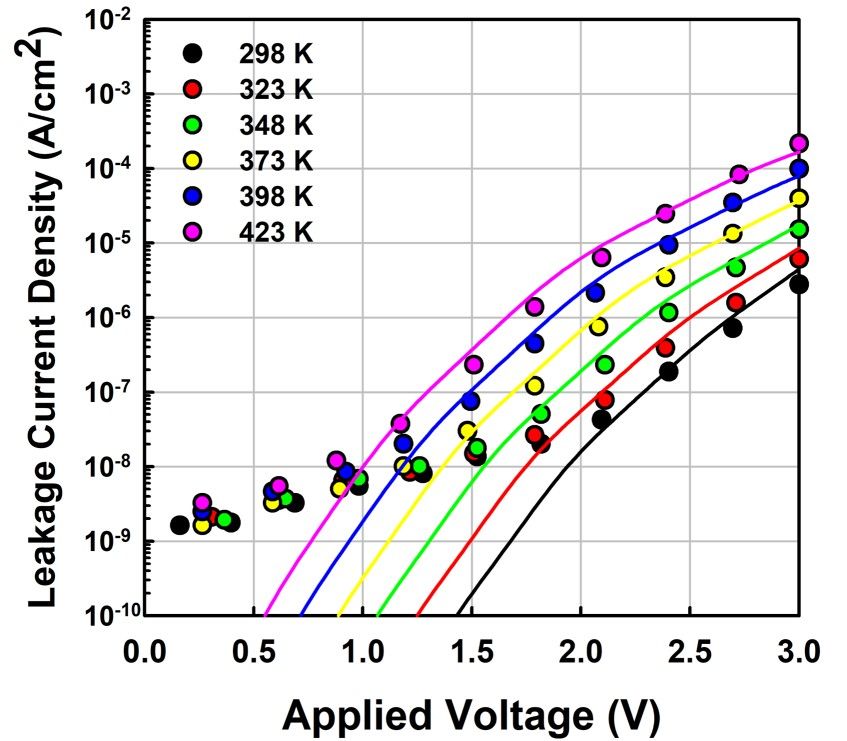
parameter. The emission rates were computed following the principle of detailed balance. Figure 1c
shows that our simulation results matched well with experimental data under various temperature
conditions. The main parameters were: TINS = 8 nm, conduction band offset (CBO) = 1.90 eV,
ETRAP = 1.1 eV, and NTRAP = 1 × 1019 cm−3 . It is worth noting that the experimental data measured
at a low electric field were ignored in our simulation as they were attributed to deep traps [19].
Only the shallow trap level, which provided the dominant leakage path formed by oxygen vacancies,
was considered [20].
The TDDB simulation was performed based on the leakage current simulation. Figure 2 shows a
flowchart of the proposed TDDB model. The TDDB simulation followed these five steps: (i) set the
initial trap distribution, structure, material parameters, and leakage current at the TDDB condition
(ILIMIT ); (ii) after the calculation of the leakage current (ILEAK ) through the trap-assisted charge transport
models, determine whether the TDDB condition is satisfied (ILEAK > ILIMIT ); (iii) if not, fill the trap
sites with electrons and calculate the electric field using the Poisson equation, which is distorted by
the trapped electrons; (iv) probe the electric fields of all nodes and calculate the new trap generation
probability based on the thermochemical model [8]; and (v) repeat the above procedure after the update
of the trap distribution using the Monte Carlo method.
In this section, the proposed reliability prediction model is explained. The leakage current of a
planar DRAM storage capacitor is simulated using the possible leakage current mechanisms of
metal/insulator/metal (MIM) structures (Figure 1a): (i) thermionic emission, (ii) Fowler–Nordheim
tunneling, (iii) Poole–Frenkel emission (PFE), (iv) trap-assisted tunneling (TAT), (v) trap-to-trap
tunneling, and (vi) direct tunneling. Figure 1b shows the structure of the simulated storage capacitor,
Micromachines 2019, 10, 256                                                                       4 of 9
which has a TiN/ZrO2/TiN stack.

                                               (ⅰ) (a) Leakage current mechanisms
                                                     (ⅱ)
                                           ETRAP           (ⅲ)
                                                                 (ⅳ)
                                  CBO
                                                   (ⅴ)
                                                      (ⅵ)

                                                                                 qV

                            Metal Dielectric Metal
        A                       (b) Structure                                                (c) Results

                                                   A'

   A                                               A'
                                           TiN
         TINS                            ZrO2
         TMETAL                            TiN

    Figure
    Figure 1.  (a) Energy
            1. (a) Energy band
                           band diagram
                                diagram ofof aa metal/insulator/metal
                                                metal/insulator/metal (MIM)
                                                                      (MIM) capacitor,
                                                                             capacitor, including
                                                                                        including the
                                                                                                  the possible
                                                                                                      possible
    charge   transport  mechanisms.      CBO:    conduction  band  offset between   the  metal
    charge transport mechanisms. CBO: conduction band offset between the metal and dielectric   and dielectric
                                                                                                       layers.
    layers. ETRAP is an energy level of a trap state. The red arrows show possible charge transport
    ETRAP is an energy level of a trap state. The red arrows show possible charge transport mechanisms:
    mechanisms: (i) thermionic emission, (ii) Fowler–Nordheim tunneling, (iii) Poole–Frenkel emission
    (i) thermionic emission, (ii) Fowler–Nordheim tunneling, (iii) Poole–Frenkel emission (PFE), (iv) trap-
    (PFE), (iv) trap-assisted tunneling (TAT), (v) trap-to-trap tunneling, and (vi) direct tunneling. The red
    assisted tunneling (TAT), (v) trap-to-trap tunneling, and (vi) direct tunneling. The red circles
    circles represent trapped electrons at the trap sites. q and V are the elementary charge and applied
    represent trapped electrons at the trap sites. q and V are the elementary charge and applied voltage,
    voltage, respectively. (b) Bird’s-eye and cross-sectional views of a simulated TiN/ZrO2 /TiN capacitor.
    respectively. (b) Bird’s-eye and cross-sectional views of a simulated TiN/ZrO2/TiN capacitor. (c)
    (c) Calibrated simulation data compared with experimental data [21]. It is worth noting that the leakage
    Calibrated simulation data compared with experimental data [21]. It is worth noting that the leakage
    current at a low bias is ignored, as only the shallow trap level, which originates from oxygen vacancies,
    current at a low bias is ignored, as only the shallow trap level, which originates from oxygen vacancies,
    is considered [20].
    is considered [20].

     The leakage currents of ZrO2-based storage capacitors are affected mainly by PFE and TAT
owing to the high defect density of ZrO2 [13,14]. In addition to the PFE and TAT, the proposed model
solved the electron and hole continuity equations coupled with the Poisson equation: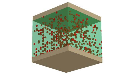
temperature conditions. The main parameters were: TINS = 8 nm, conduction band offset (CBO) = 1.90
eV, ETRAP = 1.1 eV, and NTRAP = 1 × 1019 cm−3. It is worth noting that the experimental data measured at
a low electric field were ignored in our simulation as they were attributed to deep traps [19]. Only
the shallow trap level, which provided the dominant leakage path formed by oxygen vacancies, was
Micromachines [20].
considered    2019, 10, 256                                                                         5 of 9

       Structure
     generation and                        Solve the Poisson                                   END
        meshing                              and continuity
                                               equations
                                            (calculate trap-
                                                                                                    YES
                                            assisted leakage
   Set an initial trap                          current)                               If ILEAK > ILIMIT
      distribution

                                                          t' = t + ∆t                                NO

                                          Probe the electric
                                                                                     Solve the Poisson
       Parameter                          field and generate
                                                                                    equation with filled
    calibration with                      new traps with the
                                                                                          trap sites
    experiment data                      Monte Carlo method
                                                                                   (calculate the electric
      and material                            based on a
                                                                                    field distortion due
       properties                          thermochemical
                                                                                   to trapped electrons)
                                                 model

           Figure 2. Flowchart of the proposed time-dependent dielectric breakdown (TDDB) model.
           Figure 2. Flowchart of the proposed time-dependent dielectric breakdown (TDDB) model.
3. Results and Discussion
       The
       ILIMITTDDB
                was simulation    was performed
                      calculated assuming           based on the
                                              the percolation     leakage as
                                                               condition,  current
                                                                               shown  simulation.
                                                                                         in Figure Figure      2 shows
                                                                                                       3. In this   case,
athe
   flowchart    of  the proposed   TDDB   model.   The TDDB   simulation   followed     these   five  steps:
     trap-to-trap tunneling current rapidly increased in the low-bias region, which was used to determine     (i) set the
initial
 ILIMIT . trap
           Baseddistribution,  structure, material
                   on the thermochemical     model,parameters,   andofleakage
                                                     the probability     bonding current
                                                                                   breaking at the  TDDB
                                                                                                 (PBD  ) is condition
(ILIMIT); (ii) after the calculation of the leakage current (ILEAK) through the trap-assisted charge transport
                                                            ∆H0
                                                                       !
models, determine whether the TDDB condition is satisfied            (ILEAK > ILIMIT); (iii) if not, fill the trap sites
                                              PBD = exp −        + γE                                                (12)
with electrons and calculate the electric field usingkthe    B T Poisson equation, which is distorted by the
trapped electrons; (iv) probe the electric fields of all nodes and calculate the new trap generation
where ∆H0 is the enthalpy of activation for bond breakage, kB is the Boltzmann’s constant, T is
 the temperature, γ is the field acceleration parameter, and E is the applied electric field. The main
parameters were ∆H0 = 1.874 eV and γ = 8.67 cm/MV [21]. The newly generated trap was affected
 by the existing trap. This phenomenon occurred as the existing trap became an electron trap site.
The trapped electron reduced the defect formation energy nearby, thus increasing the probability that a
 new trap would form around the existing trap [22]. The enhancement in the local electric field by the
 trapped electrons led to an increase in trap generation probability around an existing trap. Figure 4a
 shows the progression of the trap generation and occupation of TDDB according to the stress. In this
 case, the stress bias was 4.4 V for the voltage of the top electrode (V TOP ), while the temperature was
 398 K. Figure 4c–e show the trap distribution at each point in Figure 4a. Traps were generated through
probabilities based on the TDDB model and eventually reached the TDDB condition by forming a
percolation path. Furthermore, TDDB simulations were repeated in many samples, changing the stress
 bias conditions. The TDDB distribution was summarized as a Weibull plot, which was calculated as a
 cumulative probability density function (CDF), as shown in Figure 4b. Particularly, when ln(–ln(1 −
 CDF)) = 0, which represents the lifetime, the experimental [21] and simulation results were consistent.
cases. Owing to the nonuniform electric field, considering the cylindrical structure, the maximum
electric field was formed at the interface of the top electrode where the Gauss surface was small [23].
This suggests a weakness of top-electrode interface degradation. Particularly, in the edge case, the
maximum electric field was enhanced owing to the electric field crowding effect [24]; however,
simultaneously,      the minimum electric field was significantly reduced owing to the nonuniform
Micromachines 2019, 10, 256                                                                        6 of 9
electric field. Therefore, in this structure, most samples showed collapse of the body case.

      Figure 3.
     Figure   3. Calculation        ILIMIT
                   CalculationofofILIMIT    assuming
                                         assuming    thethe percolation
                                                         percolation   pathpath  is (a)
                                                                             is (a) not not formed
                                                                                        formed       or formed;
                                                                                                 or (b)  (b) formed;
                                                                                                                  (c)
     (c) corresponding
     corresponding         leakage
                       leakage       current
                               current        densities.
                                         densities. The   The
                                                        red     red
                                                            circles  circles
                                                                    representrepresent
                                                                               traps,   traps,
                                                                                      while thewhile
                                                                                                blue  the
                                                                                                     lines blue lines
                                                                                                           represent
Micromachines 2019, 2, x FOR PEER REVIEW                                                                              7 of 9
      represent
     leakage     leakage
              current     current
                        paths      paths by trap-to-trap
                              by trap-to-trap   tunneling.tunneling.

                      VTop = 4.4 V
                                                      (a)                 398 K                           (b)

                                                                                                      VTop = 4.6 V
                                                                                                      VTop = 4.4 V
                                                                                                      VTop = 4.2 V

                                                (s)                                                 (s)

                                  (c)                                      (d)                                       (e)
   TiN

   ZrO2

                                Trap
   TiN

     Figure 4.
     Figure      TDDB
              4.TDDB     simulation
                       simulation   withwith   a constant
                                           a constant        voltage
                                                        voltage       stress
                                                                 stress of 4.4ofV 4.4 V at
                                                                                  at 398 K. 398  K. (a) Leakage
                                                                                            (a) Leakage            current
                                                                                                          current density
     until the TDDB. (b) Weibull plot for the experimental (symbols) and simulation (lines) results. results.
     density  until the TDDB.   (b)  Weibull    plot for  the experimental    (symbols)   and  simulation   (lines) (c)–(e)
     (c)–(e) represent
     represent   points points
                          A–C inA–C(a),in respectively.
                                          (a), respectively.TheThe
                                                                redred  spheres
                                                                      spheres      indicatetrap
                                                                                 indicate    trapsites.
                                                                                                  sites. Trap
                                                                                                         Trap generation
                                                                                                               generation
     according to
     according   to the
                    the stress
                        stress and
                               and (e)
                                    (e) formation
                                         formation of of aa percolation
                                                            percolation path
                                                                         path were
                                                                               were observed.
                                                                                      observed.

     Finally, the TDDB simulation was extended with a 3D cylindrical structure by combining the
above simulation results. The structure was defined by: TINS = 2 nm, TMETAL = 0.5 nm, bottom critical
dimension (CDBOT ) = 10 nm, and height (H) = 20 nm, assuming an extremely scaled and simplified
capacitor, as shown in Figure 5a. Figure 5b shows the trap distribution at breakdown. In contrast to the
planar structure, the trap formation occurred mainly near the interface between the top electrode and
dielectric film. The reason for this is as follows: first, the 3D cylindrical structure shown in Figure 5a
had a smaller top electrode than a bottom one, while the planar structure had the same top electrode

     Figure 5. (a) Bird’s-eye view of the cylindrical structure. (b) Trap formation at the TDDB. The red
tBD                                                VTop = 4.6 V
                                                                                                     VTop = 4.4 V
                                                                                                     VTop = 4.2 V

                                                 (s)                                               (s)
Micromachines 2019, 10, 256                                                                                                 7 of 9
                                   (c)                                     (d)                                      (e)
    TiN
area as the bottom one. Considering Gauss’s law, this means that the electric field near the top electrode
was larger than that near the bottom electrode, which made trap formation near the top electrode
easier than near the bottom electrode. Second, the 3D cylindrical structure had two corners in the top
    ZrO2while the planar one had no corners. According to the electrostatics, a sharp corner increased
electrode
the electric field surrounding it. Thus, trap formation was relatively easy around the corners of the top
                               Trap
electrode. Figure 5c shows the electric field when V TOP = 1.0 V in the absence of a trap, while Figure 5d
    TiNthe maximum and minimum electric fields for body, edge, and planar cases. Owing to the
shows
nonuniform electric field, considering the cylindrical structure, the maximum electric field was formed
at the interface of the top electrode where the Gauss surface was small [23]. This suggests a weakness
of top-electrode   interface
      Figure 4. TDDB          degradation.
                        simulation              Particularly,
                                   with a constant            in the
                                                     voltage stress ofedge   case,
                                                                       4.4 V at 398 the maximum
                                                                                    K. (a)            electric
                                                                                           Leakage current      field was
                                                                                                             density
enhanced     owing
      until the TDDB.to (b)
                         theWeibull
                             electricplot
                                       field
                                          for crowding    effect (symbols)
                                              the experimental    [24]; however,     simultaneously,
                                                                            and simulation               the minimum
                                                                                              (lines) results. (c)–(e)
electric field  was   significantly   reduced    owing    to the   nonuniform     electric  field.
      represent points A–C in (a), respectively. The red spheres indicate trap sites. Trap generationTherefore,    in this
structure,  most  samples    showed     collapse  of the body   case.
      according to the stress and (e) formation of a percolation path were observed.

       Figure5.5.(a)
      Figure      (a)Bird’s-eye
                      Bird’s-eyeview
                                  viewof of
                                         thethe
                                             cylindrical  structure.
                                                cylindrical           (b) Trap
                                                               structure.       formation
                                                                           (b) Trap       at the at
                                                                                     formation   TDDB.   The redThe
                                                                                                    the TDDB.     region
                                                                                                                      red
      indicates  generated   traps.  (c) Electric  field contour
       region indicates generated traps. (c) Electric field TOP    (V      =  1.0 V, without  traps). (d) Summarized
                                                                       contour (VTOP = 1.0 V, without traps). (d)
      maximum
       Summarized andmaximum
                       minimum electric    fields in the
                                   and minimum           body,fields
                                                      electric   edge, in
                                                                       andthe
                                                                            planar    TOP = 1.0
                                                                                   (Vedge,
                                                                               body,        andV,planar
                                                                                                   without(Vtraps) cases.
                                                                                                             TOP = 1.0 V,

     without traps) cases.
4. Conclusions
     A full 3D TCAD-based TDDB model for DRAM storage capacitors was proposed. It can
4. Conclusion
be employed to predict leakage current and TDDB in a complex structure, which is required by
      A full 3D TCAD-based TDDB model for DRAM storage capacitors was proposed. It can be
state-of-the-art DRAM storage capacitors, based on the powerful function of TCAD. In addition, it can
employed to predict leakage current and TDDB in a complex structure, which is required by state-of-
be applied to predict characteristic changes due to structural variations, such as surface roughness
the-art DRAM storage capacitors, based on the powerful function of TCAD. In addition, it can be
and etch profile, and can be extended to a mixed-mode and AC analysis by utilizing other functions
applied to predict characteristic changes due to structural variations, such as surface roughness and
of TCAD.
etch profile, and can be extended to a mixed-mode and AC analysis by utilizing other functions of
TCAD.Contributions: W.Y.C. and G.Y. conceived, designed, and analyzed the simulations. S.S. performed the
Author
simulations. W.Y.C., Y.C., and K.H.A. managed and supervised the research project.
 Author Contributions: W.Y.C. and G.Y. conceived, designed, and analyzed the simulations. S.S. performed the
Funding:   This
 simulations.   workY.C.,
              W.Y.C.,  was and
                             supported in part byand
                                K.H.A. managed     SKsupervised
                                                      Hynix; thetheNRF  of Korea
                                                                    research      funded by the MSIT under
                                                                             project.
Grant NRF-2018R1A2A2A05019651 (Mid-Career Researcher Program), NRF-2015M3A7B7046617 (Fundamental
Technology Program), NRF-2016M3A7B4909668 (Nano-Material Technology Development Program); the IITP
funded by the MSIT under Grant IITP-2018-0-01421 (Information Technology Research Center Program); and the
MOTIE/KSRC under Grant 10080575 (Future Semiconductor Device Technology Development Program).
Conflicts of Interest: The authors declare no conflict of interest.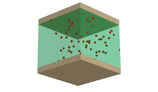
Micromachines 2019, 10, 256                                                                                       8 of 9

References
1.    Park, J.M.; Hwang, Y.S.; Kim, S.W.; Han, S.Y.; Park, J.S.; Kim, J.; Seo, J.W.; Kim, B.S.; Shin, S.H.; Cho, C.H.;
      et al. 20 nm DRAM: A new beginning of another revolution. In Proceedings of the 2015 IEEE International
      Electron Devices Meeting (IEDM), Washington, DC, USA, 7–9 December 2015.
2.    Park, S.-K. Technology Scaling Challenge and Future Prospects of DRAM and NAND Flash Memory.
      In Proceedings of the 2015 IEEE International Memory Workshop (IMW), Monterey, CA, USA, 17–20 May
      2015; pp. 1–4.
3.    Kim, D.H.; Kim, J.Y.; Huh, M.; Hwang, Y.S.; Park, J.M.; Han, D.H.; Kim, D.I.; Cho, M.H.; Lee, B.H.;
      Hwang, H.K.; et al. A mechanically enhanced storage node for virtually unlimited height (MESH) capacitor
      aiming at sub 70 nm DRAMs. In Proceedings of the IEDM Technical Digest, IEEE International Electron
      Devices Meeting, San Francisco, CA, USA, 13–15 December 2004; pp. 69–72.
4.    Deok-Sin, K.; Song, H.-S.; Kee-Jeung, L.; Hong, K.; Jin-Hyock, K.; Park, K.-S.; Seung-Jin, Y.; Jae-Sung, R.;
      Noh-Jung, K.; Hyun-Chul, S.; et al. Development of New TiN/ZrO2 /Al2 O3 /ZrO2 /TiN Capacitors Extendable
      to 45 nm Generation DRAMs Replacing HfO2 Based Dielectrics. In Proceedings of the 2006 Symposium on
      VLSI Technology, 2006. Digest of Technical Papers, Honolulu, HI, USA, 13–15 June 2006; pp. 38–39.
5.    Padmanabhan, R.; Mohan, S.; Morozumi, Y.; Kaushal, S.; Bhat, N. Performance and Reliability of
      TiO2 /ZrO2 /TiO2 (TZT) and AlO-Doped TZT MIM Capacitors. IEEE Trans. Devices 2016, 63, 3928–3935.
      [CrossRef]
6.    Kaczer, B.; Larcher, L.; Vandelli, L.; Reisinger, H.; Popovici, M.; Clima, S.; Ji, Z.; Joshi, S.; Swerts, J.;
      Afanas’ev, V.V.; et al. SrTiOx for sub-20 nm DRAM technology nodes—Characterization and modeling.
      Microelectron. Eng. 2015, 147, 126–129. [CrossRef]
7.    Kittl, J.A. High-k dielectrics for future generation memory devices. Microelectron. Eng. 2009, 86, 1789–1795.
      [CrossRef]
8.    McPherson, J.; Kim, J.; Shanware, A.; Mogul, H.; Rodriguez, J. Trends in the ultimate breakdown strength of
      high dielectric-constant materials. IEEE Trans. Devices 2003, 50, 1771–1778. [CrossRef]
9.    Jegert, G.; Kersch, A.; Weinreich, W.; Lugli, P. Monte Carlo Simulation of Leakage Currents in TiN/ZrO2 /TiN
      Capacitors. IEEE Trans. Electron Devices 2011, 58, 327–334. [CrossRef]
10.   Padovani, A.; Larcher, L. Time-dependent dielectric breakdown statistics in SiO2 and HfO2 dielectrics:
      Insights from a multi-scale modeling approach. In Proceedings of the 2018 IEEE International Reliability
      Physics Symposium (IRPS), Burlingame, CA, USA, 11–15 March 2018; p. 3A-2.
11.   Sentaurus Device Simulator. 2018. Available online: https//www.synopsys.com/silicon/tcad/device-
      simulation/sentaurus-device.html (accessed on 16 April 2019).
12.   Popescu, D.H. Modeling of Leakage Currents in High-k Dielectrics for Future DRAM Application. Doctoral
      Dissertation, Technische Universität München, Munich, Germany, 2015.
13.   Weinreich, W.; Shariq, A.; Seidel, K.; Sundqvist, J.; Paskaleva, A.; Lemberger, M.; Bauer, A.J. Detailed leakage
      current analysis of metal–insulator–metal capacitors with ZrO2 , ZrO2 /SiO2 /ZrO2 , and ZrO2/Al2O3/ZrO2 as
      dielectric and TiN electrodes. J. Vac. Sci. Technol. B 2013, 31, 1. [CrossRef]
14.   Jegert, G.; Kersch, A.; Weinreich, W.; Schröder, U.; Lugli, P. Modeling of leakage currents in high-κ dielectrics:
      Three-dimensional approach via kinetic Monte Carlo. Appl. Phys. Lett. 2010, 96, 62113. [CrossRef]
15.   Palma, A.; Godoy, A.; Carceller, J.E.; Villanueva, J.A.L.; Jimenez-Tejada, J.A. Quantum two-dimensional
      calculation of time constants of random telegraph signals in metal-oxide–semiconductor structures. Phys. Rev.
      B 1997, 56, 9565–9574. [CrossRef]
16.   Cartujo, P.; Jiménez-Molinos, F.; Gámiz, F.; Villanueva, J.A.L.; Palma, A. Direct and trap-assisted elastic
      tunneling through ultrathin gate oxides. J. Appl. Phys. 2002, 91, 5116–5124.
17.   Nasyrov, K.A.; Gritsenko, V. Charge transport in dielectrics via tunneling between traps. J. Appl. Phys. 2011,
      109, 93705. [CrossRef]
18.   Colalongo, L.; Valdinoci, M.; Baccarani, G.; Migliorato, P.; Tallarida, G.; Reita, C. Numerical analysis of
      poly-TFTs under off conditions. Solid-State Electron. 1997, 41, 627–633. [CrossRef]
19.   Pešić, M.; Knebel, S.; Geyer, M.; Schmelzer, S.; Böttger, U.; Kolomiiets, N.; Afanas’ev, V.V.; Cho, K.; Jung, C.;
      Chang, J.; et al. Low leakage ZrO2 based capacitors for sub 20 nm dynamic random access memory
      technology nodes. J. Appl. Phys. 2016, 119, 064101. [CrossRef]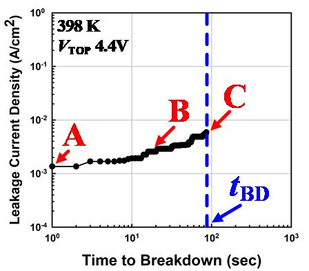
Micromachines 2019, 10, 256                                                                                    9 of 9

20.   Jegert, G.; Popescu, D.; Lugli, P.; Häufel, M.J.; Weinreich, W.; Kersch, A. Role of defect relaxation for
      trap-assisted tunneling in high-κ thin films: A first-principles kinetic Monte Carlo study. Phys. Rev. B 2012,
      85, 045303. [CrossRef]
21.   Kwon, H.-M.; Kwon, S.-K.; Jeong, K.-S.; Oh, S.-K.; Oh, S.-H.; Choi, W.-I.; Kim, T.-W.; Kim, D.-H.; Kang, C.-Y.;
      Lee, B.H.; et al. A Correlation between Oxygen Vacancies and Reliability Characteristics in a Single Zirconium
      Oxide Metal-Insulator-Metal Capacitor. IEEE Trans. Devices 2014, 61, 2619–2627. [CrossRef]
22.   Gao, D.Z.; Strand, J.; El-Sayed, A.-M.; Shluger, A.L.; Padovani, A.; Larcher, L. Role of electron and hole
      trapping in the degradation and breakdown of SiO2 and HfO2 films. In Proceedings of the 2018 IEEE
      International Reliability Physics Symposium (IRPS), Burlingame, CA, USA, 11–15 March 2018; p. 5A-2.
23.   Jackson, J.D. Classical Electrodynamics; John Wiley & Sons: Hoboken, NJ, USA, 2007.
24.   Bhattacharya, K. On the dependence of charge density on surface curvature of an isolated conductor. Phys. Scr.
      2016, 91, 35501. [CrossRef]

                         © 2019 by the authors. Licensee MDPI, Basel, Switzerland. This article is an open access
                         article distributed under the terms and conditions of the Creative Commons Attribution
                         (CC BY) license (http://creativecommons.org/licenses/by/4.0/).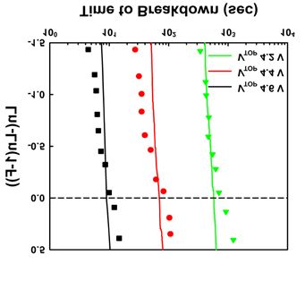
You can also read