Acoustic Doppler velocity measurement system using capacitive micromachined ultrasound transducer array technology - Tufts
←
→
Page content transcription
If your browser does not render page correctly, please read the page content below
Acoustic Doppler velocity measurement system using capacitive
micromachined ultrasound transducer array technology
             Minchul Shin and Joshua S. Krause
             Department of Mechanical Engineering, Tufts University, Medford, Massachusetts 02155

             Paul DeBitetto
             Draper Laboratory, 555 Technology Square, Cambridge, Massachusetts 02139

             Robert D. Whitea)
             Department of Mechanical Engineering, Tufts University, Medford, Massachusetts 02155
             (Received 17 May 2012; revised 28 May 2013; accepted 30 May 2013)
             This paper describes the design, fabrication, modeling, and characterization of a small (1 cm2
             transducer chip) acoustic Doppler velocity measurement system using microelectromechanical
             systems capacitive micromachined ultrasound transducer (cMUT) array technology. The cMUT
             sensor has a 185 kHz resonant frequency to achieve a 13 beam width for a 1 cm aperture. A
             model for the cMUT and the acoustic system which includes electrical, mechanical, and acoustic
             components is provided. Furthermore, this paper shows characterization of the cMUT sensor
             with a variety of testing procedures including Laser Doppler Vibrometry (LDV), beampattern
             measurement, reflection testing, and velocity testing. LDV measurements demonstrate that the
             membrane displacement at the center point is 0.4 nm/V2 at 185 kHz. The maximum range of the
             sensor is 60 cm (30 cm out and 30 cm back). A velocity sled was constructed and used to
             demonstrate measureable Doppler shifts at velocities from 0.2 to 1.0 m/s. The Doppler shifts agree
             well with the expected frequency shifts over this range. VC 2013 Acoustical Society of America.

             [http://dx.doi.org/10.1121/1.4812249]
             PACS number(s): 43.35.Yb, 43.38.Bs [MS]                                                 Pages: 1011–1020

I. INTRODUCTION                                                            fabrication and use of aluminum nitride films show promise
                                                                           for addressing these challenges, as well as providing better
     Velocity measurement systems and rangefinders are used
                                                                           process compatibility.
in a variety of applications, such as mobile robot positioning,
                                                                                In this work, we explore MEMS acoustic ultrasonic
personal navigation systems, micro air vehicle navigation,
                                                                           transducers for in-air velocity Doppler velocity measure-
obstacle detection, and map building.1–6 A number of
                                                                           ment. Limited prior work has been described for MEMS
approaches exist. Among suitable techniques, RADAR-based
                                                                           transducer systems applied to in-air acoustic range finding
Doppler velocity or distance measurement systems in the 10
                                                                           and Doppler velocity measurement. In 2010, Przybyla et al.
to 100 GHz band are often used. These systems include con-
                                                                           described a MEMS based piezoelectric acoustic rangefinder
tinuous wave (CW) systems for velocity measurement, and
                                                                           in air.9 Przybyla et al. employed a thin film aluminum nitride
frequency modulated systems for distance measurement.
                                                                           membrane in a pulse-echo range finding configuration. In
However, RADAR based systems may require high power
                                                                           the current work, a significantly different approach is taken;
consumption and a large aperture to achieve a narrow beam
                                                                           a capacitive micromachined ultrasound transducer (cMUT)
width.
                                                                           array is used in a CW mode for velocity measurement.
     Acoustic rangefinders using piezoelectric actuation
                                                                                The array described here has many similarities to other
schemes are an alternative to radio frequency (RF) devices.7
                                                                           cMUT devices, which were first described by Haller and
However, piezoelectric sensors operating in thickness mode
                                                                           Khuri-Yakub,10,11 and have since been developed by a num-
(d33) experience a limited acoustic impedance match to air,
                                                                           ber of authors.12–17 However, the majority of cMUT work has
which provides poor effective transduction between the me-
                                                                           been directed toward biomedical ultrasound or submerged
chanical and acoustical fields. The deposition of matching
                                                                           ultrasound. This paper presents the first demonstration of
layers or the careful design of bending structures using d31
                                                                           cMUT based in-air Doppler ultrasound.
mode coupling can increase efficiency.8,9 Piezoelectric
                                                                                The focus of this paper is to describe the design, fabrica-
acoustic devices designed in this manner are effective, but
                                                                                                                                              Author's complimentary copy

                                                                           tion, modeling, and characterization of a 1 cm2 planar array.
may require large actuation voltages. In addition, piezoelec-
                                                                           The sensor array has a 185 kHz resonant frequency to
tric materials can be expensive and difficult to fabricate
                                                                           achieve a 13 beam width. A model for the cMUT and the
as quality thin films when using a microelectromechanical
                                                                           acoustic system which includes electrical, mechanical, and
systems (MEMS) based approach. Recent advances in the
                                                                           acoustic components is provided. Furthermore, this paper
                                                                           provides characterization of the cMUT sensor with a variety
a)
     Author to whom correspondence should be addressed. Electronic mail:   of testing procedures. Acoustic testing, Laser Doppler
     r.white@tufts.edu                                                     Vibrometry (LDV), beampattern testing, reflection testing,

J. Acoust. Soc. Am. 134 (2), August 2013              0001-4966/2013/134(2)/1011/10/$30.00      C 2013 Acoustical Society of America
                                                                                                V                                      1011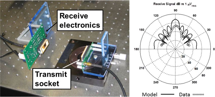
and velocity testing were used to characterize the perform-        both polysilicon layers for a total polysilicon thickness
ance of the sensors.                                               of 3.5 lm. The final step in the PolyMUMPS process is the
                                                                   deposition of a 500 nm thick layer of chrome/gold, which is
II. FABRICATION                                                    patterned by liftoff. This layer is used for electrical intercon-
                                                                   nect and the bond pads.
     The cMUT sensor array was fabricated using the                     After the chips return from the PolyMUMPsV foundry,
                                                                                                                              R
                             R
MEMSCAP PolyMUMPsV process along with facilities at                the device is released by etching the sacrificial oxide using
Tufts University in the Tufts Micro and Nano Fabrication           4:1 Hydrofluoric Acid (49%):Hydrochloric Acid (37%) mix-
Facility.                                                          ture for 150 min. Note that the addition of HCl to the release
                   R
     PolyMUMPsV is a foundry process that produces a thin          etch is critical. Without HCl, the etch rapidly attacks the
film polysilicon structure using surface micromachining            polysilicon grain boundaries, dramatically increasing series
processes. Seven physical layers, including three structural,      resistance. After the release etch, one additional Au layer
two sacrificial, and one metal layer are used in the process.      (2 lm thick) is deposited to reduce the resonant frequency of
The process is shown schematically in Fig. 1.                      the sensor. The Au layer is deposited by sputtering through a
     The fabrication procedure for the sensor begins with a        shadow mask. Next, the chip is packaged in a ceramic dual
silicon wafer with high phosphorus surface doping. Low             in-line package (DIP) using epoxy and is wire bonded. A
pressure chemical vapor deposition (LPCVD) is utilized to          small amount of epoxy was used behind the chip to attach it
deposit a 600 nm silicon nitride. After the deposition of sili-    to the package, but no epoxy was used around the sides of
con nitride, 500 nm thick polysilicon (the Poly 0 layer) is        the chip or to cover the wire bonds, in order to limit the
deposited for the building of the bottom electrode by using        packaging induced stresses in the chip. In testing, the reso-
LPCVD, and then patterned by photolithography and plasma           nant frequency of a particular element was observed to
etching. After the bottom electrode layer is deposited, a          increase from 175 kHz before packaging to 180 kHz, indicat-
2 lm oxide sacrificial layer is deposited by LPCVD and             ing that a small amount of tensile residual stress was intro-
annealed for 1 h at 1050  C. This heavily dopes the Poly 0        duced during packaging. The observed shift is acceptable,
layer. Subsequently, 750 nm deep dimples are etched in the         but further study would be needed if a large number of chips
phosphosilicate glass (PSG) using reactive ion etching             were to be produced. Figure 2 shows the schematic of the
(RIE). The anchor regions are then defined by lithography          complete sensor. Tables I and II give the geometric and
and RIE. Subsequently, 2 lm of polysilicon (Poly 1) is             material properties of the sensor structure.
deposited by LPCVD and patterned in a similar fashion.
This is the first structural layer.
                                                                   III. DESIGN AND MATHEMATICAL MODELING
     After the deposition of the first structure layer, a second
PSG layer (Oxide 2) with a thickness of 750 nm is deposited             The cMUT sensor array consists of an 8  8 pattern
and patterned. For the sensor described here, Oxide 2 is com-      where the elements are arrayed on a 1.01 cm  1.01 cm chip,
pletely removed. Following this, the second structure layer        as shown in Fig. 3. Every sensor is connected in parallel.
of polysilicon (Poly 2), with 1.5 lm thickness, is deposited       There are two bonding pads along the bottom edge of the
by LPCVD and patterned by RIE. Both polysilicon layers             chip for electrical connection. The element center-to-center
are heavily doped with phosphorous by diffusion from the           pitch is 1.1 mm. Packaging uses a ceramic DIP to which the
PSG layers. The diaphragm structure is constructed from            MEMS array is wire bonded. The device was designed with

                                                                                                   FIG. 1. (Color online) Schematic illus-
                                                                                                   trating the fabrication process using
                                                                                                                                    R
                                                                                                   the MEMSCAP PolyMUMPsV pro-
                                                                                                   cess. (1) Bare silicon substrate. (2)
                                                                                                   Silicon nitride layer is deposited as an
                                                                                                   electrical isolation layer. (3) Bottom
                                                                                                   electrode is patterned on the Poly 0
                                                                                                   layer. (4) Sacrificial oxide layer is de-
                                                                                                   posited to create the cavity. (5)
                                                                                                   Dimples are patterned into the first
                                                                                                   Oxide layer. (6) Poly 1 and Poly 2
                                                                                                                                               Author's complimentary copy

                                                                                                   layers are deposited and patterned as a
                                                                                                   diaphragm. (7) Oxide is removed
                                                                                                   through hydrofluoric acid release. (8)
                                                                                                   Au is deposited and sensor fabrication
                                                                                                   is complete.

1012    J. Acoust. Soc. Am., Vol. 134, No. 2, August 2013                      Shin et al.: Micromachined Doppler ultrasound array chip
TABLE I. Geometric properties of the microphone.

                                                                               Symbol                        Property                  Value        Units

                                                                               a                      Radius of diaphragm                300         lm
                                                                               tpoly              Thickness of polysilicon layer         3.5         lm
                                                                               tgold                 Thickness of gold layer             2.0         lm
                                                                               ahole             Radius of diaphragm vent holes          2.0         lm
                                                                               n                Number of vent holes in diaphragm        28

                                                                               which is valid at low frequencies, where ka  1. F is the
                                                                               total force from the area integral of pressure on the dia-
                                                                               phragm, Udia is the volume velocity of the diaphragm, q is
FIG. 2. (Color online) Schematic of one element in the cMUT sensor array
showing the cross-sectional diagram after Au deposition.                       the density of air, c is the speed of sound, a is the radius of
                                                                               the diaphragm, and k is the acoustic wavenumber. The result
a resonant frequency of 185 kHz, motivated primarily by the                    was derived for a circular diaphragm oscillating in a clamped
desire to achieve a 13 (66.5 about center) 3 dB beam                        static bending mode shape
width (half power) with a 1 cm aperture. The beam width                                              "    2 #2
was chosen to be similar to commercial RF Doppler                                                        r
                                                                                       uðr; tÞ ¼ U0 1           ejxt ;                               (2)
systems such as the Innosent IVS-167 (InnoSent GmbH,                                                     a
Donnersdorf, Germany). Based on stiction calculations23 and
previous experimental work with the PolyMUMPS process,                         where u(r,t) is the oscillatory surface velocity of the diaphragm.
the maximum achievable diaphragm diameter for the 3.5 lm                       The environmental acoustic impedance can be approximated
thick polysilicon structure with a 2 lm air gap that could be                  by area averaging the force
fabricated without sticking down during release was 0.6 mm.
However, this structure would have too high of a resonant                                     F        qc 1         2     29
frequency in air (400 kHz). In order to bring the resonant                         Zenv                     ðkaÞ þ 2        jka ;           (3)
                                                                                            AUdia pa2 2                 5  7p
frequency down to 185 kHz, 2 lm of gold was sputtered on
in post processing.                                                            where A ¼ pa2 is the area of the diaphragm. This impedance
     The lumped element model shown in Fig. 4 was used                         can be represented as a parallel combination of an acoustic
for design calculations.13,24 Figure 4 shows the lumped                        resistance and acoustic mass
element model (LEM) for both the mechanical and electrical
equivalent circuits. This model includes the sub-elements of                           Zenv ¼ ððMA jxÞ1 R1 1
                                                                                                          A Þ :                                       (4)
the model: External environmental air loading, cMUT struc-
tural mechanics, electromechanical coupling, backing cavity                    At low frequencies, for ka much less than 1, the values of
compliance, air damping, and the negative electrostatic                        the resistance and mass are
spring. The modeling procedure closely follows the methods
                                                                                                 qc
described by Doody et al.13 The most significant difference                            RA ¼ 0:551                                                     (5)
                                                                                                 a2
from the model of Doody et al. is that this device has holes
through the diaphragm to front vent the device.                                                  q
                                                                                       MA ¼ 0:296 :                                                   (6)
     The environmental mass loading represents the acoustic                                      a
radiation impedance of the vibrating diaphragm radiating into
an infinite half-space. The mechanical radiation impedance                     It may be possible to improve on this environmental imped-
of a circular diaphragm in an infinite baffle oscillating in the               ance using more terms in the approximation, and other meth-
static clamped mode shape is approximated by Greenspan25                       ods of averaging the pressure over the diaphragm to preserve
                                                                             power. The results of Greenspan25 and Lax26 are useful in
               F         1     2      29                                       this regard, particularly for systems that may be loaded by a
     Zmech         qc ðkaÞ þ 2           jka ;             (1)               heavy fluid where environmental impedance effects become
              Udia       2         5  7p

TABLE II. Material properties of the diaphragm.
                                                                                                                                                             Author's complimentary copy

Symbol                             Property                            Value                         Units                           Reference(s)

qpoly                      Density of polysilicon                      2320                        kg/m3                           Madou (Ref. 18)
qgold                         Density of gold                         19 300                       kg/m3                          Bauccio (Ref. 19)
Epoly                 Modulus of elasticity of polysilicon             160                          GPa                            Sharpe (Ref. 20)
Egold                   Modulus of elasticity of gold                   80                          GPa                      Rashidian and Allen (Ref. 21)
vpoly                   Poisson’s ratio of polysilicon                 0.22                     Dimensionless                      Sharpe (Ref. 20)
vgold                      Poisson’s ratio of gold                     0.44                     Dimensionless                      Gercek (Ref. 22)

J. Acoust. Soc. Am., Vol. 134, No. 2, August 2013                                      Shin et al.: Micromachined Doppler ultrasound array chip     1013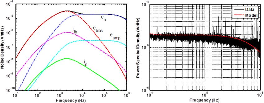
FIG. 3. (Color online) Microscope
                                                                                                      image of a single element after packag-
                                                                                                      ing using light field illumination (left)
                                                                                                      and a portion of the cMUT array using
                                                                                                      dark field illumination (right).

dominant. However, for the system presented here which                        na2hole
operates in air, the environmental impedance is not a domi-              S¼           ;                                                  (11)
                                                                               a2
nant effect.
     The damping from the air flowing through the vent holes         where l is the viscosity of air, tpoly is the thickness of the pol-
and the air flowing laterally in the cavity is also shown in         ysilicon, tgold is the thickness of gold, n is the number of
Fig. 4. The impedance is calculated as the sum of two domi-          holes in the diaphragm, ahole is the radius of the holes in the
nant resistances: The resistance for flow through the holes,         diaphragm, and S is the ratio of the open hole area to the total
which comes from the classical small pipe resistance with            diaphragm area. Note that this resistive element is in parallel
end corrections, and the squeeze film damping for a perfo-           with the cavity compliance, and thus neglects additional
rated plate, estimated using Skvor’s formula (S and Cf               squeeze damping that would be present due to air motion for
below).24,27 Homentcovschi and Miles confirm and extend              compression in the backing cavity (which would be in series
this result.28                                                       with the cavity compliance). It is assumed that the damping
                                                                     from flow to and through the diaphragm holes is dominant
       Rvent ¼ Rhole þ Rsqueeze ;                              (7)   over flow due to nonuniform compression in the gap, due to
                                                                   the relatively large and closely spaced vent holes.
                   8l                       3                             The cavity compliance represents the stiffness of the air
       Rhole ¼              tpoly þ tgold þ   pahole ;         (8)
                 npa4hole                   8                        in the backing cavity as it is compressed by the diaphragm
                                                                     during its deflection. Ccav is determined from the volume of
                    12lCf                                            the gap, Vgap divided by the product of the density of air, q,
       Rsqueeze ¼           ;                                  (9)
                    npt3gap                                          and the speed of sound, c, squared.

              S 3 S2 1 pffiffiffi                                                       Vgap
       Cf ¼       lnð SÞ;                                  (10)       Ccav ¼        :                                                 (12)
              2 8 8 2                                                             qc2

                                                                                                      FIG. 4. Coupled mechanical-electrical
                                                                                                      lumped element model.
                                                                                                                                                  Author's complimentary copy

1014      J. Acoust. Soc. Am., Vol. 134, No. 2, August 2013                       Shin et al.: Micromachined Doppler ultrasound array chip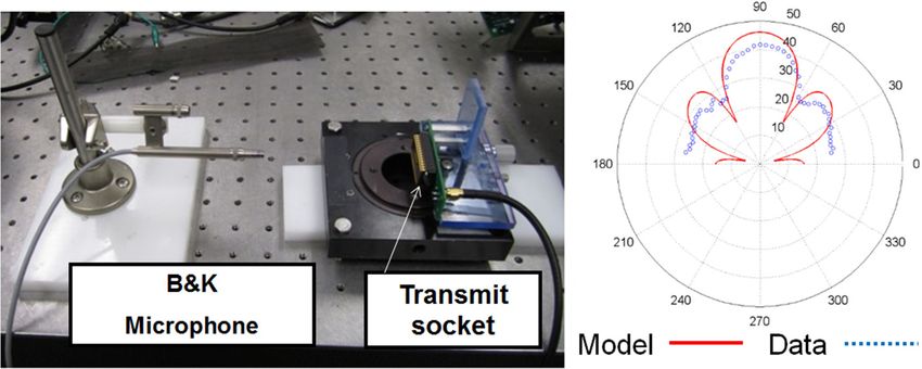
The compliance of the diaphragm (for a two layer thin lami-          drive frequency. This frequency doubling effect is caused by
nate clamped circular bending plate) with the effective bend-        the quadratic nature of the electrostatic coupling.
ing stiffness of the gold layer and the polysilicon diaphragm,            The electrostatic spring compliance is, when a dc bias is
and the effective mass of the diaphragm (for the first mode          used,
of the same two layer thin laminate clamped circular bend-
ing plate) are computed using the classical thin laminate                           t3gap
                                                                         Celect ¼    2 e
                                                                                              ;                                     (22)
plate theory                                                                        Vbias 0

               pa6 1                                                 or, in transmit mode with pure ac drive,
     Cdia ¼                 ;                                (13)
              16  12 Deff
                                                                                  16t3gap
              X Ei            t3i                                        Celect ¼     2e
                                                                                             :                                      (23)
                                         2                                           Vac
     Deff   ¼                     þ t i yi ;                 (14)                        0
               i
                   1   2i 12
         X  E i ti                                                 Modeling of the electrostatic coupling and the negative elec-
            zi                                                       trostatic spring follow the methods of Doody et al.13 Two
          i
                1   2i                                             LEMs of a single cMUT element were used, as can be seen
     yc ¼ X              ;                                   (15)
                 E i ti                                              in Fig. 4. The top model shows the component in “transmit”
            i
               1   2i                                              mode. In this mode, the input voltage, Vac, is driven on the
                                                                     left side of the model as a voltage source. The output of this
     y i ¼ zi  y c ;                                        (16)    mode is the diaphragm volume velocity, Udia and vent hole
                                                                     volume velocity, Uvent. It is emphasized again that, for a
               9ðqpoly tpoly þ qgold tgold Þ
     Mdia ¼                                  ;               (17)    pure ac voltage drive with zero dc bias, all mechanical quan-
                          5pa2                                       tities (such as diaphragm volume velocity) will be at twice
                                                                     the drive frequency due to the quadratic nature of the elec-
where i is an index for the layer type (polysilicon or gold), yc
                                                                     trostatic coupling. It is possible to compute the pressure in
is the position of the neutral axis with respect to the bottom
                                                                     the farfield by summing the baffled monopole fields trans-
of the laminate, yi is the distance from the center of the ith
                                                                     mitting from all of the array elements
layer to the neutral axis, and zi is the position of the center of
the ith layer with respect to the bottom of the laminate. Ei,                        XN
                                                                                          1
vi, ti, and qi are the elastic modulus, Poisson ratio, thickness,        P ¼ jqf             ðUdia  Uvent ÞejkRm HðhÞ;          (24)
                                                                                         R m
and density of the ith layer, respectively. Deff is the effective                    m¼1
bending stiffness of the laminate plate. Mdia and Cdia are the
final results of the calculation, the effective diaphragm mass,      where Udia - Uvent is the net source volume velocity: The dif-
and compliance.                                                      ference between the diaphragm volume velocity and the flow
      The coupling from the mechanical to electrical side via        through the vent holes. These volume velocities are com-
the ideal transformer is shown in Eqs. (18) and (19) where           puted from the LEM of a single transducer, k ¼ x/c is the
P1 is the effective electrostatic pressure, V1 is the voltage        acoustic wavenumber, f is the transmit frequency in cycles/s,
across the electrodes, I1 is the current flow through the            q is the density of air, and Rm is the scalar distance from the
capacitor, and Udia is the volume velocity of the diaphragm.         center of the mth array element to the field point. H(h) is the
                                                                     directivity of an individual element. At the drive frequency
     P1 ¼ N  V1 ;                                           (18)    of 185 kHz, ka is close to unity, so the individual elements
                                                                     are somewhat directional.
     I1 ¼ N  Udia :                                         (19)         The beampattern of a baffled piston is used to approxi-
                                                                     mate the beampattern of the individual elements,
When operating in receive mode, the cMUT array is held
at a constant dc bias, Vbias. When operating in transmit                            2J1 ðkaeff sin hÞ
mode for electrostatic (laser vibrometry testing) a voltage              HðhÞ ¼                       ;                             (25)
                                                                                      kaeff sin h
V(t) ¼ Vbias þ Vacejxt is applied to the system. In these cases
the coupling factor is                                               where h is the angle, measured from the normal, to the field
            Vbias e0                                                 point, and J1 is the Bessel function of the first kind, order 1.
     N¼              :                                       (20)    For the purposes of directivity calculation, the effective
             t2gap
                                                                     radius, aeff, of the transmitting element should be used.
                                                                                                                                           Author's complimentary copy

In acoustic transmit mode, the cMUT array is driven with a           Since the element deforms as a circular bending plate, the
pure ac drive, V(t) ¼ Vacejxt and the coupling factor is             effective radius of an equivalent baffled piston is somewhat
                                                                     less than the physical radius. An effective radius equal to
            Vac e0                                                   70% of the physical radius is a good approximation. This
     N¼            ;                                         (21)
            4t2gap                                                   was determined by a finite element computation of the beam-
                                                                     pattern projected into an infinite half space by a baffled
where Vac is the amplitude of the ac drive signal. In this case      clamped axisymmetric circular plate oscillating in the
all mechanical signals in the linear LEM will be at twice the        clamped static mode shape given in Eq. (2). The individual

J. Acoust. Soc. Am., Vol. 134, No. 2, August 2013                        Shin et al.: Micromachined Doppler ultrasound array chip   1015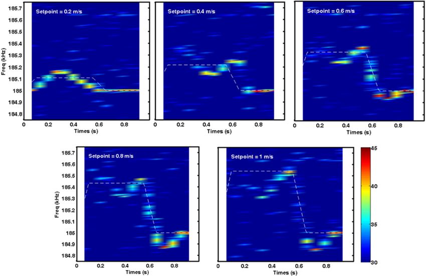
IV. EXPERIMENTAL RESULTS
To investigate the dynamic behavior of the sensor mem-
branes, LDV was first used to test the electromechanical fre-
quency response. The laser spot was directed to the center of
each membrane. A frequency sweep was driven using a sig-
nal generator, with an applied dc bias and ac voltage. The
vibratory displacement response of the cMUT sensor array
was measured by LDV. A comparison between predicted
frequency response results and measurement is shown in
Fig. 5. The magnitude is normalized to the product of the
applied dc bias and ac bias during electrostatic drive. This
choice of normalization is made to emphasize that it is this
product which is proportional to electrostatic force at the
drive frequency. Measured frequency response by LDV is in
excellent agreement with model predictions. As expected,
the resonant frequency decreased to approximately 185 kHz
FIG. 5. (Color online) Predicted center point motion frequency response for after a 2 lm gold layer was deposited by shadow masking.
a single element and the experimental result.
Before the deposition of Au, the resonant frequency of the
membrane is 430 kHz. All 64 elements in the array were
elements are not strongly directional at the frequency of measured in this fashion. For the transmitter chip, the aver-
operation, so the array beampattern is not strongly affected age value of the resonant frequency of 64 elements is
by small changes to the effective radius. The summation is 180.26 kHz and the standard deviation is 3.97 kHz, with
over the 64 array elements. Since all the elements are identi- 61/64 element yield. The average phase at the peak is
cal, all the Udia Uvent are the same, and only the distance to 113 , with a standard deviation of 5.2 . For the receiver
the field point, Rm, changes. This transmit model neglects chip, the average value of the resonant frequency of 64 ele-
any acoustic coupling between the elements. ments is 193.74 kHz and the standard deviation is 3.69 kHz
The bottom picture shows the component in “receive” with 58/64 element yield. The average phase at the peak is
mode. In receive mode, an acoustic pressure, Pin, is deliv- 118 with a standard deviation of 7.3 . For both chips, the
ered from the environment, vibrating the diaphragm of the quality factor (Q) is 9.
receiver. The output of the receive mode is the current flow- Second, a free field acoustic beampattern measurement
ing on the electrical side, which is integrated by the charge was conducted for the array relative to a reference micro-
amplifier to produce the measured voltage output. In the phone. As shown in Fig. 6, on the transmit side, a rotary
charge amplifier, Cfb is 150 pF and Rfb is 10 MX, resulting in positioner was used to incrementally rotate the cMUT trans-
a high pass filter cutoff of 5 kHz for the preamplifier stage. mit chip about its center. The beampattern, also shown in
Following the charge amplifier, the signal is passed into a se- Fig. 6, was measured at 10 cm from the source (in the far field
ries of two operational amplifier based inverting amplifier of the array, but still within the direct field), using a B&K 14
circuits with single pole high pass filters. The second and in. free field microphone (Bruel and Kjaer, Denmark). The
third amplifier stages are based on the OP27 low noise voltage drive to the cMUT was 20 Vpeak-to-peak at 40 kHz.
operational amplifier (Analog Devices, Norwood, MA), each Frequency doubling due to the electrostatic drive produced
configured with a gain of 20 dB and a bandwidth of 2 to acoustics at 80 kHz. The measurement was conducted in CW
800 kHz. The low frequency cutoff is determined by discrete operation at 80 kHz. This test was run below the designed
components in the high pass filter design, and the high fre- operating frequency of the cMUT (185 kHz) because the
quency cutoff is set by the gain bandwidth product of the B&K cannot measure above 100 kHz. Results show a beam-
amplifier in combination with the designed gain of 20 dB. pattern very similar to model predictions. The measured
Author's complimentary copy
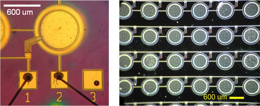
FIG. 6. (Color online) Acoustic trans-
mit test using cMUT array (80 kHz).
Experimental setup (left) and beampat-
tern (right). Beampattern is in units of
dB SPL.
1016 J. Acoust. Soc. Am., Vol. 134, No. 2, August 2013 Shin et al.: Micromachined Doppler ultrasound array chip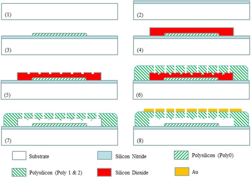
FIG. 7. (Color online) Acoustic trans-
                                                                                                   mit and receive testing using two
                                                                                                   cMUT arrays at 185 kHz. Experimental
                                                                                                   setup (left) and beampattern (right).

response was 40 dB sound pressure level (SPL) (re 20 lParms)     CW transmit and receive using two chips reflecting off a flat
(rms ¼ root-mean-square) at 10 cm on axis.                       aluminum plate show a maximum range of 60 cm (30 cm out
     A second free field measurement was conducted using a       and 30 cm back) as shown in Fig. 8. Signal power decreases
pair of cMUT chips. The experimental setup and results are       with the square of D as expected. With D 30 cm, the signal
shown in Fig. 7. The transmit chip was driven electrically at    decreases below the noise floor (91 dB Vrms). In this experi-
92.5 kHz drive with 20 Vpeak-to-peak. Again, frequency dou-      ment, the sampling frequency was Fs ¼ 1 MHz and the num-
bling due to square law electrostatics gave acoustics at         ber of samples was 2,21 resulting in a total data acquisition
185 kHz. This has the advantage of reducing electromagnetic      time of 4.2 s per point. The resulting noise bandwidth is
interference (EMI) from direct RF transmission, which is         0.24 Hz.
primarily at 92.5 kHz. Driving at half frequency with pure ac         Figure 9 shows a schematic of the preamplifier electron-
is an effective and simply implemented method of reducing        ics including all electronic noise sources. The contributions
EMI contamination of the results. The transmitter was on the     to the total noise from each component in the electronics
rotary positioner. The dc bias on the receiver was 10 V. The     have been analyzed. Each noise source is uncorrelated, and
transducer arrays were 10 cm apart. The measured response        so can be considered separately. Linear circuit theory, using
was 0.5 mVrms (53 dB re 1 lVrms) at peak, which compares         an ideal op-amp model for the AD8065, can be applied to
reasonably well with the predicted 2.5 mVrms from the com-       determine the transfer functions for each term. The total
putational model. The discrepancy in absolute level could be     noise can be added in a rms sense. The various contributions
due to a combination of factors including mismatches             to the total noise, at the AD8065 output, are
between the two array chips, imperfect alignment during
testing, and scattering off of the test structures. The 3 dB                   Zf b Csensor jx
beam width (half power) is as expected at 13 (6.5 on either        Vebias ¼                             ebias ;                  (26)
                                                                           1 þ Rfilt ðCfilt þ Csensor Þjx
side of the center). The side lobes are down by 15 dB com-
pared to the main lobe.                                                        Zf b Csensor jxð1 þ Rfilt Cfilt jxÞ
                                                                     Ven ¼ 1 þ                                       en ;          (27)
     To investigate the achievable range of a reflected acous-                  1 þ Rfilt ðCfilt þ Csensor Þjx
tic wave, range testing with a reflecting boundary was con-
ducted, as shown in Fig. 8. During range testing experiments,        Vin ¼ Zf b in ;                                               (28)
the angle of the transducers was adjusted at each distance D         Vif b ¼ Zf b if b ;                                           (29)
in order to maximize the return signal. The lateral distance
between the array chips was 10 cm. There was an acrylic
                                                                 where the feedback impedance is the parallel combination of
plate in between the arrays to prevent direct transmission
                                                                 the feedback components
between the chips. As in the previous experiment, the drive
signal was 20 Vpp at 92.5 kHz, and the dc bias on the receiver                     Rf b
                                                                     Zf b ¼                    :                                   (30)
side was 10 V. Experimental results for reflected acoustic                    1 þ Rf b Cf b jx
                                                                                                                                            Author's complimentary copy

                                                                                                   FIG. 8. (Color online) Reflection test
                                                                                                   using cMUT array. Sensor signal is in
                                                                                                   dB Vrms in a 0.24 Hz band (4.2 s aver-
                                                                                                   aging time).

J. Acoust. Soc. Am., Vol. 134, No. 2, August 2013                    Shin et al.: Micromachined Doppler ultrasound array chip      1017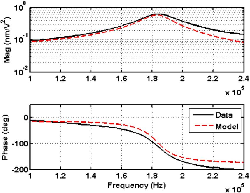
TABLE III. Electrical elements in the noise model.

                                                                                       Symbol                   Property                       Value        Units

                                                                                       Csensor        MEMS sensor capacitance                    4            nF
                                                                                       Rfilt                  Filter resistor                    1           kX
                                                                                       Cfilt                 Filter capacitor                   10            lF
                                                                                       Cfb                Feedback capacitor                    150           pF
                                                                                       Rfb                 Feedback resistor                    10           MX
                                                                                                    Low frequency band limit for the             2           kHz
                                                                                       f1                    bandpass filter
                                                                                                     High frequency band limit for              800          kHz
                                                                                       f2                  the bandpass filter
FIG. 9. (Color online) Schematic of the preamplifier electronics including
electronic noise sources.                                                              G              Gain of the bandpass filter                100
                                                                                       k                  Boltzmann constant                1.38  1023     J/K

The component values are given in Table III. The noise con-
tributions are acted on by the transfer function of the two
                                                                                       Figure 9 shows the contribution of each noise source and the
stage bandpass filter downstream of the AD8065. This band-
                                                                                       rms total of the noise sources as a whole. As can be seen
pass filter is constructed using two OP27 operational ampli-
                                                                                       from Fig. 9, the system noise near the 185 kHz operating fre-
fiers. The first of these amplifiers contributes additional
                                                                                       quency is dominated by the voltage noise of the preamplifier
noise, eamp. The resulting noise densities add in an rms sense
                                                                                       chip. The noise model is directly compared to a measure-
to produce the total noise density estimate at the output of
                                                                                       ment of the system output noise density in Fig. 10, with
the electronics
                                                                                       excellent agreement. This suggests that the major noise sour-
               qffiffiffiffiffiffiffiffiffiffiffiffiffiffiffiffiffiffiffiffiffiffiffiffiffiffiffiffiffiffiffiffiffiffiffiffiffiffiffiffiffiffiffiffiffiffiffiffiffiffiffiffiffiffiffiffiffiffiffiffiffi          ces in the system have been captured. Voltage noise domi-
       Vout ¼ G     2 þ V 2 þ V 2 þ V 2 þ e2
                   Vbias         Ven           if b         in        amp              nates current noise, bias noise, and thermal noise for this
                                                             2                       particular system, thus the noise density at the system output
                                   jx
                                                                                     can be estimated from the preamplifier voltage noise ampli-
                                 2pf1
                                                     ;                 (31)   fied by the preamplifier gain and bandpass stage gain,29
                  1 þ jx                1þ
                                                    jx

                         2pf1                    2pf2                                                     Cs

                                                                                            enoise ¼ en 1 þ        G;                           (33)
                                                                                                             Cf b
where G is the passband gain of the bandpass amplifier,                                                   pffiffiffiffiffiffi
f1 and f2 delineate the bandwidth of the bandpass filter,                              where en ¼ 7 nV/ Hz is the AD8065 voltage noise density,
       pffiffiffiffiffiffiffiffiffiffiffiffiffiffiffiffiffi                                                              Cs ¼ 4 nF is the sensor capacitance, Cfb ¼ 150 pF is the feed-
if b ¼ 4kT=Rf b , is the Johnson noise from the feedback
                           pffiffiffiffiffiffi                                                     back capacitance of the preamp, and G ¼ 100 is the passband
resistor, eamp ¼ 3 nV/ Hz is OP27 voltage noise, en
          pffiffiffiffiffiffi                  pffiffiffiffiffiffi                                             gain of the second and third stage amplifiers. Thispsimpleffiffiffiffiffiffi
¼ 7 nV / Hz, and in ¼ 0.6 fA/ Hz, are the voltage and cur-                             model results in an estimated noise floor of 20 lV/ Hz at
rent noise from the AD8065, respectively. The values for                               the system output, identical to the value measured near
einst, en, and in come from the data sheets (Analog Devices,                           185 kHz.
Norwood, MA). Also according to the datasheet of the                                        In the final set of tests, a velocity sled was constructed
REF01 10 V reference IC (Analog Devices, Norwood,                                      and used to demonstrate measureable Doppler shifts at
MA), the bias voltage noise has a low frequency noise den-                             velocities from 0.2 to 1.0 m/s. The velocity test setup con-
                   pffiffiffiffiffiffi
sity of 3 lV/ Hz, and exhibits a 1/f dependence at high                                sists of a speed controller, a dc motor, a shaft encoder, and a
frequencies. It is well modeled by                                                     moving sled, as shown in Fig. 11. The transmitter faces the
                                                                                       receiver. The tests were conducted with the transmitter
                     pffiffiffiffiffiffi           2pð10 kHzÞ                                      moving and the receiver stationary, so no reflections were
       ebias ¼ ð3 lV= HzÞ                            :                          (32)
                                     2pð10 kHzÞ þ jx                                   needed; this improved the signal-to-noise ratio. A continuous

                                                                                                                           FIG. 10. (Color online) Results of
                                                                                                                                                                     Author's complimentary copy

                                                                                                                           noise computations showing (left) rela-
                                                                                                                           tive contributions of the noise sources
                                                                                                                           to the noise power spectral density
                                                                                                                           (right) comparison of the total pre-
                                                                                                                           dicted noise to the measured noise
                                                                                                                           density.

1018      J. Acoust. Soc. Am., Vol. 134, No. 2, August 2013                                          Shin et al.: Micromachined Doppler ultrasound array chip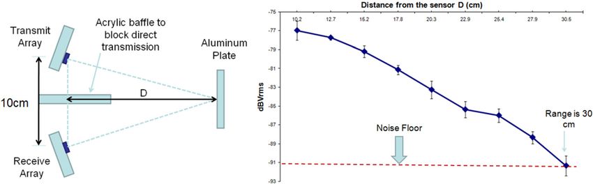
FIG. 11. (Color online) Experimental
                                                                                                  setup for velocity test (left), and an
                                                                                                  example spectrogram and sled velocity
                                                                                                  command (right).

acoustic wave at 185 kHz was sent from the transmitter           some spread of velocities during the motion, due to the fluc-
while the sled accelerated toward the receiver, held at a con-   tuation of the sled velocity about the set point.
stant velocity, and then decelerated back to a stop. The con-         Figure 12 shows similar spectrograms as the com-
troller controls the velocity and distance of the sled,          manded velocity of the sled changes between 0.2 and 1 m/s.
communicating with the dc motor.                                 The Doppler shift increases as the velocity of the sled
     The receiver output voltage was recorded for 1 s dur-       increases. A good match is obtained between the measured
ing each test with a sampling rate of 500 kHz. The sled          Doppler shift and velocity of the transmitter. The dynamics
velocity command accelerates for 0.1 s, holds a constant         of the sled motion are apparent in the spectrograms; over-
velocity for 0.45 s, decelerates for 0.1 s, and then stays       shoot, undershoot, and oscillation about the set point can be
stopped for the remaining 0.35 s. The controller attempts        seen. This appears to be a real velocity variation of the sled.
to follow this velocity set point, feeding back off the shaft    Figure 13 shows the average and standard deviation (as ver-
encoder. Spectrograms were computed from the received            tical error bars) of measured velocity of the sled as computed
cMUT signal using a short time Fourier transform. A              from the Doppler shift for each test. The measurement is
Hamming window with 50% overlap was used to window               compared, via the dashed line, to the nominal velocity of the
the data in each time window. Time windows consisting of         sled. The averages and standard deviations were computed
216 data points were used, resulting in windows that were        by taking the peak frequency from the spectrogram at 6
0.13 s long.                                                     times between 0.2 and 0.5 s. The horizontal error bars indi-
     Figure 11 shows an example spectrogram as time runs         cate the maximum and minimum velocity of the sled as
for a particular speed (0.6 m/s), and a sketch of the corre-     determined from shaft encoder data in a second run. The
sponding expected frequency shift as computed from the           Doppler system appears to accurately measure sled velocity,
commanded sled velocity profile. A Doppler shift is clearly      within the uncertainty in the velocity, which is due primarily
seen, following the shape of the velocity profile. There is      to real sled velocity fluctuations during the run.

                                                                                                  FIG. 12. (Color online) Spectrograms
                                                                                                  of the shifted signal during different
                                                                                                  velocity tests. Results are plotted in dB
                                                                                                  re 1 lV2/Hz. White dashed lines show
                                                                                                  the expected frequency based on the
                                                                                                                                              Author's complimentary copy

                                                                                                  sled velocity set point.

J. Acoust. Soc. Am., Vol. 134, No. 2, August 2013                    Shin et al.: Micromachined Doppler ultrasound array chip        1019
approach,” in Proceedings of the IEEE International Conference on
Robotics and Automation, pp. 1244–1249 (1998).
4
K. J. Kyriakopoulos and G. C. Anousaki, “Simultaneous localization and
map building for mobile robot navigation,” IEEE Rob. Autom. Mag. 6,
42–53 (1999).
5
C. Y. Lee, H. G. Choi, J. S. Park, K. Y. Park, and S. R. Lee, “Collision
avoidance by the fusion of different beam-width ultrasonic sensors,” in
Proceedings of IEEE Sensors, pp. 985–988 (2007).
6
O. Manolov, S. Noikov, P. Bison, and G. Trainito, “Indoor mobile robot
control for environment information gleaning,” in Proceedings of the
IEEE Intelligent Vehicles Symposium, pp. 602–607 (2000).
7
S. E. C. Biber, E. Shenk, and J. Stempeck, “The Polaroid ultrasonic rang-
ing system,” in Proceedings of the 67th Audio Engineering Society
Convention (1980).
8
M. I. Haller and B. T. Khuri-Yakub, “1-3 composites for ultrasonic air
transducers,” in Proceedings of the IEEE Ultrasonics Symposium, pp.
937–939 (1992).
9
R. Przybyla, S. Shelton, A. Guedes, I. Izyumin, M. Kline, D. Horsley,
and B. Boser, “In-air range finding with an AlN piezoelectric micro-
FIG. 13. Comparison of measured and commanded velocity during the nom-
machined ultrasound transducer,” IEEE Sensors J. 11, 2690–2697
inally constant velocity portion of the motion (from t ¼ 0.2 to t ¼ 0.5 s). The
(2011).
plotted point is the velocity as computed from the mean detected frequency 10
M. I. Haller and B. T. Khuri-Yakub, “A surface micromachined electro-
for each set point. The horizontal error bars span the maximum to minimum
static ultrasonic air transducer,” in Proceedings of the IEEE Ultrasonics
velocity for each run as determined from shaft encoder data. The vertical
Symposium, pp. 1241–1244 (1994).
error bars span one standard deviation of detected frequency above and 11
M. I. Haller and B. T. Khuri-Yakub, “A surface micromachined electro-
below the mean.
static ultrasonic air transducer,” IEEE Trans. Ultrason. Ferroelectr. Freq.
Control 43, 1–6 (1996).
12
V. CONCLUSION O. Ahrens, A. Buhrdorf, D. Hohlfeld, L. Tebje, and J. Binder, “Fabrication
of gap-optimized CMUT,” IEEE Trans. Ultrason. Ferroelectr. Freq.
An in-air acoustic Doppler velocity measurement sys- Control 49, 1321–1329 (2002).
13
tem using MEMS cMUT array technology was developed C. B. Doody, C. Xiaoyang, C. A. Rich, D. F. Lemmerhirt, and R. D.
White, “Modeling and characterization of CMOS-fabricated capacitive
and characterized with a variety of experiments. The array micromachined ultrasound transducers,” J. Microelectromech. Syst. 20,
operates at 185 kHz and is 1 cm2 in size. LDV measurements 104–118 (2011).
14
demonstrate that the membrane displacement at center point P. C. Eccardt, K. Niederer, T. Scheiter, and C. Hierold, “Surface microma-
is 0.4 nm/V2 at 185 kHz. Beampattern measurements show a chined ultrasound transducers in CMOS technology,” in Proceedings of
the IEEE Ultrasonics Symposium, pp. 959–962 (1996).
13 3 dB (half power) beam width (6.5 either side of cen- 15
I. Ladabaum, X. Jin, H. T. Soh, A. Atalar, and B. T. Khuri-Yakub,
ter). The side lobes are 15 dB below the main lobe. These “Surface micromachined capacitive ultrasonic transducers,” IEEE Trans.
results are all in good agreement with theoretical models. 16
Ultrason. Ferroelectr. Freq. Control 45, 678–690 (1998).
Experimental results for reflected acoustic CW transmit and G. Caliano, R. Carotenuto, A. Caronti, and M. Pappalardo, “cMUT echo-
graphic probes: Design and fabrication process,” in Proceedings of the
receive using two chips reflecting off a flat aluminum plate IEEE Ultrasonics Symposium, pp. 1067–1070 (2002).
show a maximum range of 60 cm (30 cm out and 30 cm 17
X. Zhuang, I. Wygant, D. S. Lin, M. Kupnik, O. Oralkan, and B. Khuri-
back). Electronic noise in the preamplifier dominates the Yakub, “Wafer bonded 2-D CMUT arrays incorporating through-wafer
trench-isolated interconnects with a supporting frame,” IEEE Trans.
noise spectrum, and is well modeled using an op-amp noise
Ultrason. Ferroelectr. Freq. Control 56, 182–192 (2009).
model. A velocity sled was constructed and used to demon- 18
M. J. Madou, Fundamentals of Microfabrication: The Science of
strate measureable Doppler shifts at velocities from 0.2 to Miniaturization (CRC Press, Boca Raton, FL, 2002), 294 pp.
19
1.0 m/s. The Doppler shifts agree well with the expected fre- M. Bauccio, ASM Metals Reference Book, 3rd ed. (ASM International,
Materials Park, OH, 1993), 154 pp.
quency shifts over this range. The major challenges for a 20
W. N. Sharpe, Jr., in The MEMS Handbook, edited by M. Gad-el-Hak
system of this type appear to be range limitations. Future (CRC Press, Boca Raton, FL, 2002), 24 pp.
21
work will focus on optimizing the sensor and electronics to B. Rashidian and M. G. Allen, “Electrothermal microactuators based on
increase the signal-to-noise ratio for increased range, partic- dielectric loss heating,” in Proceedings of the 6th IEEE Micro Electro
Mechanical Systems Conference, MEMS’93, Atlanta, GA, pp. 24–29
ularly by reducing sensor stray capacitance to reduce elec- (1993).
tronic noise sources in the preamplifier. 22
H. Gercek, “Poisson’s ratio values for rocks,” Int. J. Rock Mech. Min. Sci.
44, 1–13 (2007).
23
ACKNOWLEDGMENTS C. Mastrangelo, “Adhesion-related failure mechanisms in micromechani-
cal devices,” Tribol. Lett. 3, 223–238 (1997).
24
This work was supported by Draper Laboratory under L. L. Beranek, Acoustics, 1996 ed. (Acoustical Society of America, New
the University Research and Development program. York, NY, 1996), pp. 47–177.
25
M. Greenspan, “Piston radiator: Some extensions of the theory,”
J. Acoust. Soc. Am. 65, 608–621 (1979).
Author's complimentary copy
1 26
G. Hueber, T. Ostermann, T. Bauernfeind, R. Raschhofer, and R. M. Lax, “The effect of radiation on the vibrations of a circular dia-
Hagelauer, “New approach of ultrasonic distance measurement technique phragm,” J. Acoust. Soc. Am. 16, 5–13 (1944).
27
in robot applications,” in Proceedings of the 5th International Conference Z. Skvor, “On acoustical resistance due to viscous losses in the air gap of
on Signal Processing, pp. 2066–2069 (2000). electrostatic transducers,” Acustica 19, 295–297 (1967).
2 28
Y. Ando and S. Yuta, “Following a wall by an autonomous mobile robot D. Homentcovschi and R. N. Miles, “Viscous damping of perforated
with a sonar-ring,” in Proceedings of the IEEE International Conference planar micromechanical structures,” Sens. Actuators, A 119, 544–552
on Robotics and Automation, pp. 2599–2606 (1995). (2005).
3 29
J. A. Castellanos, J. M. Martinez, J. Neira, and J. D. Tardos, “Simultaneous B. Carter, in Op Amps for Everyone, 2nd ed., edited by R. Mancini
map building and localization for mobile robots: A multisensor fusion (Elsevier, NY, 2003), pp. 138–139.
1020 J. Acoust. Soc. Am., Vol. 134, No. 2, August 2013 Shin et al.: Micromachined Doppler ultrasound array chipYou can also read