Introduction to transmission electron microscopy - Chris Boothroyd School of Materials Science and Engineering - NTU
←
→
Page content transcription
If your browser does not render page correctly, please read the page content below
Introduction to transmission electron microscopy
                      Chris Boothroyd

         School of Materials Science and Engineering
              Nanyang Technological University
                          Singapore

                    FACTS short course
                   1530, 10 October 2018
Introduction
What is electron microscopy?
Electron means we use electrons to form our image. Electrons behave as
waves just like light, but have a much shorter wavelength.
Microscopy means we are looking at images of small things

Why use electrons not light?
Electrons have a much shorter wavelength than light. You cannot see
anything smaller than half the wavelength of the radiation you are using

What about other forms of radiation?
X-rays and neutrons can give diffraction patterns but cannot (easily) be
focused to form images
Introduction
Penetration of radiation and sample size
Depends on mean free path

        Neutrons                 X-rays       Electrons

        50 mm                   20 mm          200 nm
       millimetres             millimetres   nanometres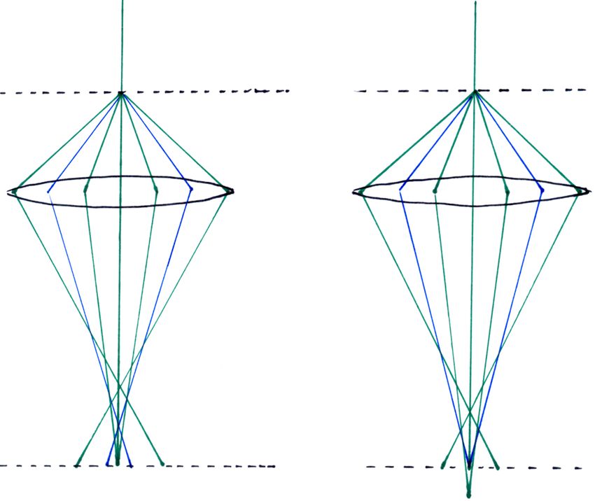
Introduction
Techniques and acronyms

EM: Electron microscopy. Covers TEM, SEM,
STEM, etc                                    SEM

SEM: Scanning electron microscopy. Collect
the secondary electrons emitted from the
surface.
                                             TEM
TEM: Transmission electron microscopy

STEM: Scanning transmission electron
microscopy. Like TEM, but scan a finely
                                             STEM
focused beam of electrons across the
specimen rather than image using a broad
beam

(STM/AFM): Scanning tunnelling microscopy/
Atomic force microscopy
                                             STM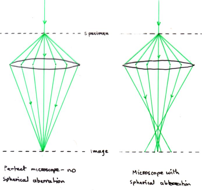
History
History
Optical microscopy: Resolution limited by wavelength of light to ~300nm
Other radiation (X-rays, γ-rays) cannot be focussed.
1897: JJ Thompson discovers the electron
1925: de Broglie proposes electrons are waves with
small wavelength
1927: Electron diffraction demonstrated by CH
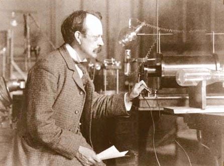
JJ Thompson, Cavendish Labs
Davisson and Lh Germer (reflection) and GP
Thompson and A Reid (transmission)
Electron diffraction from Ni surface Davisson and Germer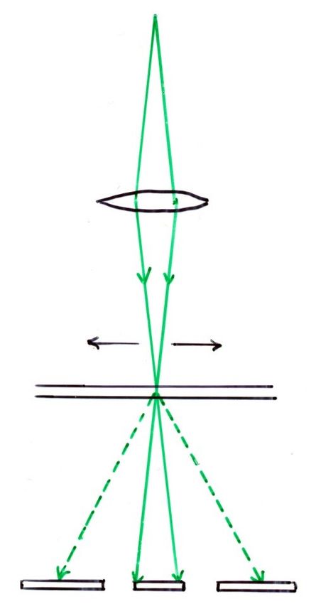
History
1931: M Knoll and E Ruska build first electron microscope
M Knoll and E Ruska, Das Elektronenmikroskop. Z. Physik 78 (1932) 318-339

                                                           Ruska &
                                                           Knoll,
                                                           1931

          First TEM image, magnification 17.4×, 50kV
http://ernst.ruska.de/daten_e/library/documents/999.nobellecture/lecture.html   Ruska’s sketch of first TEM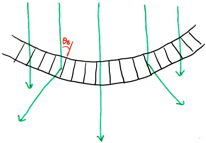
History
1934: Resolution of electron microscope better than light microscope – Driest
      & Muller
1936: First commercial TEM – Metropolitan-Vickers AEI EM1
1938: First practical commercial TEM – von Borries & Ruska, Siemens. 10 nm
      resolution. M von Ardenne builds first STEM
1940: RCA TEM, 2.4 nm resolution
1941: First electron micrographs of viruses
1942: First SEM built by Zworykin et al
1945: Resolution 1 nm

                                  Luria and
                                  Anderson, first
                                  TEM image of a
                                  bacteriophage,
                                  1942

                                                           Siemens TEM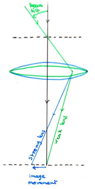
History
Electron microscope resolution

                                                   Light microscope:
                                                   resolution limit ~300nm

                                                   TEM with aberrations:
                                                   resolution limit ~0.15nm

                                                   Atomic spacings
                          “Aberration corrected”
                           electron microscope     Best TEM today:
                                                   resolution 0.05nm

                                                   Electron microscope:
                                                   resolution limit should be
                                                   ~0.001nm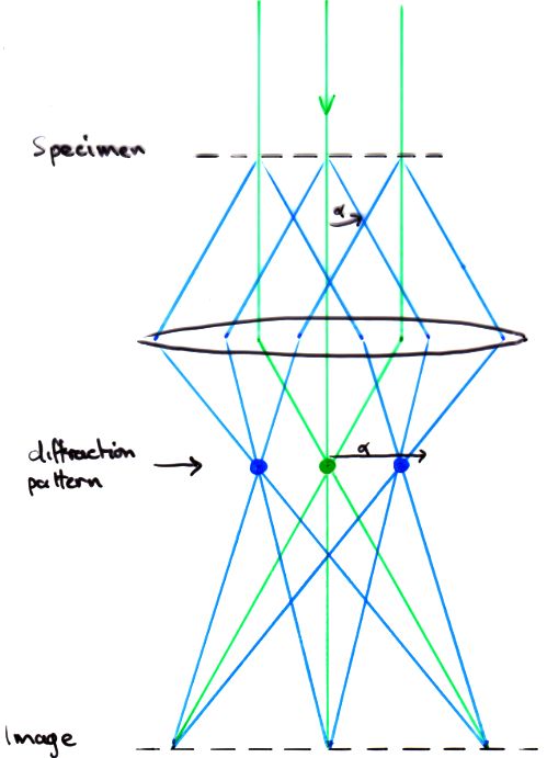
Electrons
Electron beams
Accelerating voltage and wavelength
Electrons accelerated through a potential V gain energy
   E = eV
Wavelength
                  h                                      e = electron charge
    λ=                                  (Relativistic)   me = electron mass
                  (
            2me eV 1 +     eV
                         2 me c 2   )                    c = speed of light
                                                         h = Planck constant

 Typical wavelengths
 20kV        0.0086nm
 100kV       0.0037nm
 300kV       0.0020nm

 200kV electrons are travelling at 70% of the speed of light
Electron beams Electrons are particles... Track of single electron in bubble chamber
Electron beams
Electrons are waves...
Electron diffraction pattern from Si
Electron beams
Electrons are waves...
Interference fringes from electron biprism                    Electron beam

                                                               Charged wire
                                             –            +                   –

                                                 Interference pattern
How the TEM works
How the TEM works
General principles
A TEM looks through a thin section of a
                                               Accelerating voltage
specimen (cf SEM looks at the surface)
Its principle is similar to a transmission
optical microscope                           Electron gun

                                             Electron beam
                      Lenses to focus
                     beam on specimen
                                                 Detector(s)
           Deflector coils to
           move/scan beam
                                Specimen

                           Lenses to form
                             image (TEM)

               Viewing screen (TEM)

                                                Vacuum system
How the TEM works
General principles
Electron gun
Condenser
lenses
Specimen
Objective lens
Intermediate
lenses
Viewing screenHow the TEM works Electron gun Electron gun held at accelerating voltage of typically 100 to 400kV Electron gun can be W, LaB6 or field- emission
How the TEM works
Electron sources
Two basic types
Thermionic emission source is heated until electrons overcome work
function. Normally either a tungsten wire (cheap) or a crystal of LaB6 (brighter)

             W wire filament                       LaB6 crystal filament
How the TEM works
Electron sources
Field emission source is a sharp tungsten tip. Electrons are extracted by a
high electric field. Needs a high vacuum
Gives high coherence and small spot sizes for analysis
W field emission sourceHow the TEM works
Electron guns
Electron guns extract electrons from filament and focus electrons into beam
(few kV)
(100–400kV)
Thermionic electron gun Field emission gun (FEG)How the TEM works Condenser lenses Normally 2 (or 3) condenser lenses, C1 and C2 Use C2 to control area illuminated Use C1 to change spot size (for C1 analysis) C2
How the TEM works
Specimen
Must be thin enough for electrons to pass
through (
How the TEM works
Objective lens
First magnification of the specimen
Microscope resolution depends
mainly on the quality of the objective
lens
The “focus” knob adjusts this lens
How the TEM works
Electron lenses
                    Electrons are charged
                    particles so are deflected
                    by magnetic field
                    Electrons travelling parallel
                    to magnetic field feel no
                    force
                    Electrons travelling at an
                    angle are deflected
                    sideways, so they go round
                    in a helix
                    Focusing is caused by the
                    bent part of the field at the
                    top and the bottom
                    But - the focusing is not
                    very good!
How the TEM works
Electron lenses: aberrations
Electrons going through the
edge of the lens are bent too
much. This gives rise to
spherical aberration
The spherical aberration is so
bad that even with the best lens
available today only electrons
focused within 10mrad (0.6°) of
the optic axis are focused
correctly onto the image
A good optical microscope can
focus light rays that are within
45° of the optic axis
Thus the electron beam must be accurately aligned along the centre of
all lensesHow the TEM works Objective aperture Used to select beam(s) to form image Excludes electrons scattered to high angles In diffraction plane
How the TEM works
Selected area aperture
Used to select part of an image to form
diffraction pattern
In image plane
How the TEM works
Magnifying lenses
Further magnify image formed by the
objective lens
Project image onto fluorescent screen
Also can be set to project diffraction
pattern on screen
Magnification changed by changing
strengths of these lenses
How the TEM works
Viewing screen
Fluorescent screen (emits light when
hit by electrons)
How the TEM works
Camera
Photographic plates (old microscopes)
CCD camera (recent microscopes)
How the TEM works
Alignments
Alignments are more important for TEM than for SEM. In an SEM poor
alignment means a blurry image. In a TEM, especially at high-resolution, much
more subtle image defects occur when poorly aligned
Most of the alignments are designed to put the beam on the optic axis and
keep it there
Alignments are performed by using deflectors as in an SEM, pairs of magnetic
coils that deflect the beam.
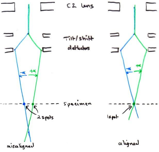
How the TEM works
Alignments: tilt purity
Tilt purity means that when the beam is tilted, it will not move across the
specimen. This is most often used in dark-field images. It is also important for
high-resolution images when aligning the beam tilt
                                          On Philips/FEI microscopes these
                                          are called “pivot points”, on JEOL
                                          microscopes “x and y wobblers”

                                          Tilt beam through angle α, when
                                          misaligned 2 spots are seen. When
                                          aligned the beam remains stationary
How the TEM works Alignments: beam tilt and rotation centre Shift and tilt purity alignments ensure that a shift is just a shift and a tilt is just a tilt Next we have to tilt the beam so it is on the optic axis. This is called setting the rotation centre. When the beam is tilted, the image moves when the focus (objective lens strength) is changed. When the beam is on the optic axis there is no movement of the image There are 3 ways of setting the rotation centre, current centring, voltage centring and the coma- free alignment. All three try to do the same thing ie get the beam on the optic axis, so you can only do one of them. But they all give a slightly different answer! The rotation centre alignment needs the tilt purity to be set correctly
How the TEM works
Alignments: defocus
Defocus is a measure of how
far out of focus the image is.
Focus is controlled by the
current in the objective lens
A positive defocus, +Δf,
means the objective current is
stronger than required for
focus, ie “overfocus”
A negative defocus, –Δf,
means the objective current is
weaker than focus, ie
“underfocus”                     at focus
                                            underfocus
How the TEM works Alignments: astigmatism Ideally electron lenses are Electrons passing through different perfectly round. Real lenses are sides of the lens focused by different not quite round and have slightly amounts different focal lengths for electrons travelling in different directions Astigmatism is corrected with the x and y stigmators, which are 2 quadrupole lenses just below the objective lens
Interaction of electrons with materials
Interaction of electrons with materials
Beam-specimen interactions: electron microscopy (SEM and TEM)

Signals emitted when a beam of
electrons hits a specimen
Many of these signals are used in
SEM or other techniques
In TEM we are concerned with the
transmitted and diffracted electrons

Elastic scattering: no energy lost,
no other radiation emitted
Inelastic scattering: some energy
lost, usually other radiation emitted
(eg X-rays, secondary electrons)
Interaction of electrons with materials
Elastic scattering: Rutherford scattering

                                      The scattering of one particle off
                –
                                      another was first considered by
                                      Rutherford when investigating
                                      scattering of Au by α particles
  –
                                      For an electron (energy E0) being
                Z+                    scattered by an atom of atomic
                                      number Z the differential cross-
                                      section (ie probability of scattering to
                            –         a particular angle, θ) is

                                             d σ (θ )        e 4Z 2
                                                      =
           –                                   dΩ       16(E0 )2 sin 4 ( θ 2 )
Interaction of electrons with materials
Elastic scattering: Rutherford scattering
d σ (θ ) e 4Z 2
=
dΩ 16(E0 )2 sin 4 ( θ 2 )
For small angles this approximates to
d σ (θ ) e 4Z 2
= 2 4
dΩ (E0 ) θ
Thus scattering goes as:
atomic number, Z, squared (for all scattering angles)
1/(scattering angle, θ)4 (for small scattering angles)Techniques
Techniques
Beam-specimen interactions

                                 100 – 300kV electrons
                                                               X-rays

                  Specimen
Techniques
Diffraction and imaging of crystals
If the specimen is thin and periodic, it acts like a diffraction grating giving
diffracted beams at angles ±α
The electron wavelength is typically Electrons
λ = 0.01 to 0.04Å
~1Å
Typical atom spacings of ~1Å give
scattering angles, α, of 0.1 to 1° Atoms
To form an image of the atoms, we
need to collect and focus at least
the electrons scattered to the first
diffraction spotsTechniques
Diffraction and imaging: Abbé theory
Electrons diffracted by To image the
the specimen are atomic structure,
focused to the diffraction we need to
pattern, and then to the collect and focus
image all the diffracted
electrons
Objective lens
Objective
aperture
Selected area
apertureTechniques Bright-field images TEM specimens are mostly transparent to electrons - they are like glass! Most of the electrons go straight through, very few are absorbed by the specimen. Thus at low magnifications there is very little contrast. Normally an objective aperture is used around the central (000) beam to increase the contrast and exclude all the diffracted beams. This gives a bright- field image The contrast in bright-field images is diffraction contrast - strongly diffracting areas are dark
Techniques
Bright-field images

                                  Aperture around unscattered beam
                                  Cuts out scattered electrons

                                                          Diffraction pattern after
                                    Diffraction pattern   objective aperture

                      Objective
                      aperture

                                                                    Bright-field
                                                                    image
Techniques
Dark-field images
Aperture around diffracted beam
Strongly diffracting areas bright
Diffraction pattern after
Diffraction pattern objective aperture
Objective
Objective
aperture
aperture
Dark-field
imageTechniques
Bright-field and dark-field images
General microstructure
Crystallography
Phases present
Grain sizes and identification
Pd-Er annealed on SiTechniques
Diffraction patterns
Switching between
Diffraction pattern
diffraction and imaging is
done by changing the
strength of the first Image
intermediate lens
Diffraction pattern Image
Diffraction mode Image modeTechniques Diffraction patterns: single crystals Electron microscope specimens are thin (
Techniques
Diffraction patterns: single crystals
Measuring d spacing                      λ ≈ d 2θB = dα
                                         x = Lα
                                         so
                          d
                                         xd = Lλ

                                         L = distance from specimen to
                                         screen (“camera length”)
                                         Lλ = “camera constant”

            L
                                                          x

                      x
                                Screen
Techniques Diffraction patterns: polycrystalline materials When there are many crystals present the diffraction patterns from each crystal are superimposed giving rings These are exactly analogous to X-ray powder diffraction patterns Identification of the materials present is like that for X-rays Measure the d spacing of the rings Compare with those of suspected materials Use X-ray powder diffraction file, ICDD PDF (Joint committee on powder diffraction standards, JCPDS, now International centre for diffraction data, ICDD)
Techniques
Diffraction patterns: amorphous materials
Amorphous materials have no crystalline structure, atoms are arranged with
no long range order
Examples: amorphous oxides (eg SiO2), metallic glass, much biological
material
Diffraction pattern has little structure

                                             Overall shape from atomic scattering
                                             factor(s)
                                             Usually 1 or 2 broad peaks from
                                             short range order (bond length)

Amorphous +                                Amorphous
polycrystalline
Techniques
High-resolution images
Objective aperture limits resolution, so remove
All beams contribute to image (little diffraction
contrast)
Contrast is phase contrast - interference
between beams
Objective Diffraction pattern
aperture
High-resolution
imageTechniques
High resolution (HREM)
Best case: projection of
atomic columns
Identification of nano-
particles
Fe2O3
Atomic structure Fe2O3
Fe
Fe
Si
Fe3O4 on SiTechniques
Convergent beam (CBED): strain measurement
Position of HOLZ lines depends on
lattice parameter
Requires simulations
Si [111]
Si [112] Toh Suey LiTechniques X-ray spectroscopy (EDX, EDS) Analyse energy of X-rays from irradiated area Determine compositions for elements with Z ≥ B
Techniques
X-ray mapping
Scan beam using STEM and measure X-ray spectrum at each point
Mapping is slow!

            Al                         Ti                  Fe
                         Ti-Al alloy containing Fe, V, B
Techniques
Energy loss spectroscopy (EELS)
Energy lost is
Energy loss spectrum from Ni3Al
characteristic of elements
present
Can analyse Z ≥ Li
Can also deduce chemical
state from shape of edge
Energy loss (eV)Techniques
Energy filtered imaging (EFTEM)
Zero loss filtering
Removes inelastic scattering leaving clearer and more quantitative image
Useful for eg strain measurement with CBED, thick polymer samples
Zero loss filtering (Si 110 diffraction pattern)Techniques
Energy filtered imaging (EFTEM)
Core loss mapping
Map elements present by their energy
loss edges
Gives elemental maps similar to X-ray
mapping
Elemental maps of
Fe-O/Cu-O/SiTechniques
STEM
Electron
Scan a finely focused beam of beam
electrons across the specimen
Collect electrons transmitted
through the specimen Objective lens
Scan
beam
Specimen
DetectorsTechniques
STEM and high angle annular dark-field (HAADF, Z contrast)
Bright-field STEM allows positioning of small
probes and mapping
Annular dark-field images all dark-field beams
HAADF images only high-angle beams,
intensity ∝ Z2
HAADF good for finding heavy elements
HAADF image of InAs layers in InP
High-resolution HAADF
NTU, Tim White
Simple projection of atomic
structure
Experiment Simulation Apatite La10(SiO4)6O2 a = 9.7Å (JEOL/NTU)Techniques
Tomography
3D reconstruction
Requires many images plus software reconstruction
Bright-field or HAADF
Magnetic particles in bacteria
University of CambridgeTechniques
Holography C Boothroyd and R Dunin-Borkowski
ZrB12 (a = 7.41 Å) Ultramicroscopy 98 (Jan 2004) 115
(200)
3.7Å (020) DiffractogramTechniques
Holography
Amplitude and phase from previous hologramTechniques Cryo-EM For biomaterials – freeze sample in ethane at 77K, transfer to microscope while cold. Sample is embedded in amorphous ice Polymersomes (polymeric vesicles) formed via the self assembly of the di-block copolymer Polyethelene glycol (0.6kDa)– Polybutadiene (1.2kDa) in water at concentration of 1mM Sample prepared in FACTS and image taken on our Zeiss Libra at 120kV by Lim Pei Qi
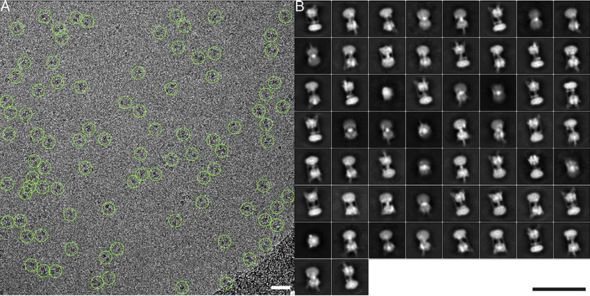
Techniques
Single particle cryo-EM
Reconstruct 3D molecular structure from thousands of single particle images

Typical cryo-EM micrograph,       58 2D classes from 77,612
      particles circled                    particles                      Final reconstructed structure

                     Sara Sandin and Andrew Wong, NTU (Davies et al, J Structural Biology 197 (2017) 350–353)
Techniques
In-situ microscopy & environmental TEM (ETEM)
Deposition of metals on sample
Sample heating in UHV
Gas reactions
Electrical biasing
Observations of liquids
TEM observations and video
recording of all of the above Before Ni deposition
Nucleation of Ni-Ge on Ge 001
After 18.3 mins Ni deposition at 300°CImage contrast
Image contrast
Mass-thickness contrast
Contrast: difference in intensity between two adjacent areas

Mass-thickness contrast occurs in
amorphous materials
Elements with higher Z scatter more
(Rutherford scattering)
In a bright-field image only collect
transmitted electrons

                Ordering in polymers. Dark
                areas contain iodine
Image contrast
Diffraction contrast
For crystalline materials, areas that diffract strongly appear dark in bright-field
Lattice planes
No diffraction Strong diffraction
Bright Dark
Bright-field image Dark-field image
Polycrystalline
Fe-SiImage contrast
Two beam condition
A “two beam condition” is when there are only two strong beams in the
diffraction pattern, the transmitted (000) beam and one diffracted beam
A two beam condition happens when
Lattice planes only one set of lattice planes is
correctly oriented to diffract
θB Two beam conditions are often used
because they are simpler to analyse
000
Examples: imaging dislocations and
defects
000
Diffraction patternImage contrast Bend contours If the crystal is bent (most are) some areas will diffract strongly These are bend contours Each diffraction spot gives one bend contour If you tilt the crystal, the bend contours move
Image contrast
Thickness fringes
Wedge shaped crystals show thickness
fringes when there is strong diffraction
This is particularly so at a two beam
condition
They are caused because intensity
oscillates between the transmitted and
diffracted beams
If you tilt the crystal, the thickness fringes
change their spacing

       Dark-field            Bright-field
Image contrast
Dislocations
Dislocations are visible when there is strong
diffraction (normally a two beam condition)
They cannot be seen when there is no
diffraction
Dislocations are invisible when
g.b = 0
g = hkl of strongly diffracting beam (not
necessarily the beam the aperture is around)
b = Burgers vector of dislocation
g.b = 0
dislocation invisibleImage contrast
Dislocations
Dislocations in Si-Ge
Bright-field Dark-field
Dislocations remain in the same place when the crystal is tiltedSpecimen preparation
Specimen preparation

For the best images the specimen needs to be:
Thin, ideally around 20nm thick
Supported, so that it doesn’t move
Stable under the beam. Many materials suffer electron damage
Clean, ie free from hydrocarbons that cause carbon contamination
Free from amorphous layers. These can be due to contamination, oxidation,
ion beam milling etc
Specimen preparation
Brittle samples (eg minerals)
Grind sample in methanol. Collect particles on carbon coated copper grid.
Quick and easy. Sometimes not much thin area

Metals
Electropolish using jets of electrolyte. Gives very clean samples (usually).
Need to mechanically grind and polish first

Semiconductors and many other materials
Ion milling using Ar+ ions. Also need to mechanically grind and polish first

Specific location (eg semiconductor devices)
Focused ion beam milling (FIB). A sophisticated version of ion milling using
Ga+ ions. Can cut an individual gate out of a device

See Williams and Carter chapter 10 for more
You can also read