Nonlinear increase, invisibility, and sign inversion of a localized fs-laser-induced refractive index change in crystals and glasses - Nature
←
→
Page content transcription
If your browser does not render page correctly, please read the page content below
Lapointe et al. Light: Science & Applications (2020)9:64                                                                                    Official journal of the CIOMP 2047-7538
                                    https://doi.org/10.1038/s41377-020-0298-8                                                                                                                        www.nature.com/lsa

                                     ARTICLE                                                                                                                                                    Open Access

                                    Nonlinear increase, invisibility, and sign inversion of
                                    a localized fs-laser-induced refractive index change
                                    in crystals and glasses
                                    Jerome Lapointe 1, Jean-Philippe Bérubé1, Yannick Ledemi                                                1
                                                                                                                                             , Albert Dupont1, Vincent Fortin1,
                                    Younes Messaddeq1 and Réal Vallée1

                                      Abstract
                                      Multiphoton absorption via ultrafast laser focusing is the only technology that allows a three-dimensional structural
                                      modification of transparent materials. However, the magnitude of the refractive index change is rather limited,
                                      preventing the technology from being a tool of choice for the manufacture of compact photonic integrated circuits.
                                      We propose to address this issue by employing a femtosecond-laser-induced electronic band-gap shift (FLIBGS), which
                                      has an exponential impact on the refractive index change for propagating wavelengths approaching the material
                                      electronic resonance, as predicted by the Kramers–Kronig relations. Supported by theoretical calculations, based on a
                                      modified Sellmeier equation, the Tauc law, and waveguide bend loss calculations, we experimentally show that several
                                      applications could take advantage of this phenomenon. First, we demonstrate waveguide bends down to a
                                      submillimeter radius, which is of great interest for higher-density integration of fs-laser-written quantum and photonic
                                      circuits. We also demonstrate that the refractive index contrast can be switched from negative to positive, allowing
                  1234567890():,;
1234567890():,;
                  1234567890():,;
1234567890():,;

                                      direct waveguide inscription in crystals. Finally, the effect of the FLIBGS can compensate for the fs-laser-induced
                                      negative refractive index change, resulting in a zero refractive index change at specific wavelengths, paving the way
                                      for new invisibility applications.

                                    Introduction                                                                                        the refractive index that occurs in most crystals5 and in a
                                       Femtosecond (fs) laser inscription in transparent                                                wide variety of glasses6–8. In fact, many applications, such
                                    materials has unique advantages1,2. One of the most                                                 as waveguide lasers9, electro-optic modulators10, and
                                    relevant advantage is the micrometer-scale processing of                                            frequency converters11, require multi-scan-depressed
                                    complex three-dimensional structures, owing to the                                                  cladding structures, which complicate or impede the
                                    nonlinear nature of the laser absorption that precisely                                             fabrication or their guiding circuits.
                                    confines structural changes to the focal volume. However,                                              In most applications of photonics, the propagating
                                    a severe limitation of fs-laser inscription is related to the                                       wavelengths are far from the material resonances to
                                    relatively low photoinduced refractive index contrast that                                          minimize the optical losses; the fiber-optic communica-
                                    is achievable3,4. In particular, the miniaturization of many                                        tion window around 1550 nm in fused silica is a good
                                    fs-laser-processed photonic devices is limited by the                                               example. Away from resonances, the compaction and
                                    minimum bend radius of waveguides, which in turn                                                    rarefaction of the structural network (affecting the num-
                                    depends on the magnitude of the induced refractive index                                            ber of charged particles per volume unit) and other
                                    contrast. Another important limitation is the decrease in                                           mechanisms such as color centers, a change in the fictive
                                                                                                                                        temperature, and defect-induced density changes largely
                                                                                                                                        dominate the refractive index change in fs-laser-processed
                                    Correspondence: Jerome Lapointe (jerome.lapointe@copl.ulaval.ca)
                                    1
                                     Centre d’Optique, Photonique et Laser, 2375 Rue de la Terrasse, Université                         photonic circuits1,6,12. However, for propagating
                                    Laval, G1V 0A6 Québec, QC, Canada

                                    © The Author(s) 2020
                                                        Open Access This article is licensed under a Creative Commons Attribution 4.0 International License, which permits use, sharing, adaptation, distribution and reproduction
                                                        in any medium or format, as long as you give appropriate credit to the original author(s) and the source, provide a link to the Creative Commons license, and indicate if
                                    changes were made. The images or other third party material in this article are included in the article’s Creative Commons license, unless indicated otherwise in a credit line to the material. If
                                    material is not included in the article’s Creative Commons license and your intended use is not permitted by statutory regulation or exceeds the permitted use, you will need to obtain
                                    permission directly from the copyright holder. To view a copy of this license, visit http://creativecommons.org/licenses/by/4.0/.
Lapointe et al. Light: Science & Applications (2020)9:64                                                                    Page 2 of 12

wavelengths approaching the electronic resonance, we           relies on different physical processes. First, a physical
show that the refractive index change exponentially            rearrangement of the structural network was observed1,20.
increases owing to a fs-laser-induced band-gap shift           It is believed that the densification induced by various
(FLIBGS). For the first time, to the best of our knowledge,     complex phenomena, such as a fast temperature
the effect of the FLIBGS in transparent materials is stu-      change21,22 and plasma shock waves23,24, has a great
died. Note that the propagating wavelengths are studied        impact on the fs-laser-induced refractive index change.
near the resonance, which are not to be confused with the      Another process is related to the variation in the
wavelength used to process the material with the fs laser      absorption spectrum through the Kramers–Kronig rela-
(producing the FLIGBS) that is far from the resonance          tions25. Increased absorption due to photoinduced defects
(fixed at 795 nm in this work). For the remainder of the        such as color centers26,27 produced by self-trapped exci-
paper, the stated wavelengths refer to light propagating in    tons28 leads to a variation in the refractive index. Since
the waveguides.                                                most of the defects can be annealed while a partial
  Using this FLIGBS phenomenon, we demonstrate that            refractive index change remains29, defects can only par-
the sign of the refractive index contrast can be inverted,     tially explain the laser-induced refractive index change.
which allows for the direct inscription of smooth wave-          To date, no one has explicitly studied the effect of the
guides (i.e., type I-positive refractive index change) in      FLIBGS on the refractive index. A first way of
crystals. This type of inscription has several advantages      approaching this problem is via the Kramers–Kronig
over structures based solely on the stress induced by          relations, relating the refractive index to the absorption
damage tracks traditionally inscribed in crystals5 or glas-    coefficient α integrated over frequency:30
ses6–8 using high-energy laser pulses (i.e., the so-called
                                                                                         Z    þ1
type III modifications13). Moreover, preliminary results                            π                αðω0 Þ
                                                                   nðωÞ ¼ 1 þ        }                      dω0                       ð1Þ
show potential invisibility applications. The opposition                           c      0        ω02  ω2
between the fs-laser-induced negative refractive index
change and the positive refractive index change due to the     where c is the speed of light, ω′ is the angular frequency
FLIBGS can result in a zero refractive index change at         variable running through the whole integration range, and
specific wavelengths, which theoretically enable invisi-        ℘ denotes the Cauchy principal value. Clearly, from this
bility. While invisibility cloaking has gained much atten-     relation, a change in the absorption α(ω′) curve will in
tion in recent years14,15, mostly due to metamaterials16,17,   turn affect n(ω). To illustrate this effect, Fig . 1 shows the
the FLIGBS mechanism demonstrates a new concept for            transmission spectrum through a zinc selenide (ZnSe)
the direct fabrication of invisible structures, paving the     crystal with a thickness of d = 1 mm (gray curve,
way for new invisibility applications. Finally, we demon-
strate a lower propagation loss in tightly curved wave-
guides mostly due to the high refractive index change
induced by the FLIBGS, which creates opportunities for
miniaturized devices. Supported by theoretical analysis,
we experimentally demonstrate waveguide bends with a
submillimeter radius of curvature, which is an important
improvement over the minimum 10-mm radius reported
previously3,18. It is somehow implicit that the use of the
FLIBGS results in a practical range of applications char-
acterized by a narrow spectral band near the resonance of
the material. Surprisingly, the FLIBGS affects the refrac-
tive index over a certain region beyond the absorption
edge bandwidth in the highly transparent region, which
extends the application range. Moreover, since electronic
bandgaps lying in the ultraviolet, visible, and infrared
regions can be found in different materials19, the FLIBGS
                                                                Fig. 1 Left axis: refractive index of ZnSe as a function of the
has great potential for the entire spectral band in             propagating wavelength using the Sellmeier coefficient from ref. 33
photonics.                                                      (black curve). Potential effects of the fs-laser-induced variation in the
                                                                number of charged particles per volume unit (blue dashed curve) and
Results                                                         the FLIBGS (green dotted curve), based on Eq. 4. Right axis: ZnSe
FLIBGS theory and experiment                                    transmission spectrum (gray curve). The double gray arrows show the
                                                                potential absorption variation in the FLIBGS window if a shift in the
  The ultrafast laser-induced refractive index change of        absorption edge occurs (dashed gray curve)
transparent materials is a complex phenomenon that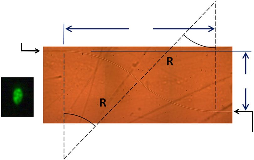
Lapointe et al. Light: Science & Applications (2020)9:64                                                            Page 3 of 12

associated with the right axis). When a band-gap shift           effect of fs-laser irradiation is suggested:
occurs, the absorption edge (near the electronic reso-
nance) of the transmission spectrum shifts horizontally.                       X ðBk þ dNk Þλ2                  ðB1 þ dN1 Þλ2
For illustrative purposes, a dashed gray curve has been          n2irr ¼ A þ                            Aþ
added to represent the shifted spectrum. At a wavelength                        k   λ2  ðCk þ dλk Þ2         λ2  ðC1 þ dλ1 Þ2
near the absorption edge (where the transmission slope is                                                                   ð4Þ
significant, denoted by the FLIBGS window in Fig. 1), the
shift greatly affects the absorption (double gray arrows)        where dNk is proportional to the laser-induced variation
and thus the refractive index.                                   in the number of charged particles per volume unit and
   Equation 1 is not convenient to use experimentally since      dλk is the laser-induced resonance shift (linked to the
it requires measurements over a very wide spectral band.         FLIGBS). The remaining terms (k > 1) are assumed to be
Alternatively, the Lorentz dispersion relation with the          negligible for wavelengths relatively close to the λ1 (or C1)
Clausius–Mossotti form allows one to express the                 electronic resonance, which is the case in this work. The
refractive index in terms of the number of charged par-          fs-laser-induced refractive index contrast is Δn = nirr − n,
ticles per volume unit Nk31:                                     where nirr is the refractive index of the irradiated region.
                                                                    For illustrative purposes, Fig. 1 shows the ZnSe refrac-
                                                                 tive index curve with the Sellmeier coefficients A = 4, B1
    3ðn2  1Þ X 4πNk ε2k =mk                                      = 1.90, and C1 = 336.15 nm from ref. 33 (black curve,
             ¼                                             ð2Þ
    ðn2 þ 2Þ   k
                 ω20k  ω2 þ iγω                                 associated with the left axis). The effects of the variation
                                                                 in the number of charged particles per volume unit (blue
                                                                 dashed curves with dN1 = ±0.1) and the FLIBGS (green
where n is the complex refractive index and mk is the
                                                                 dotted curves with dλ1 = ±30 nm), both exaggerated to
mass of particle k with charge εk. The number of charged
                                                                 clearly observe their effect over the full spectrum, are
particles per volume unit Nk, the resonance frequency
                                                                 plotted. The variation in the number of charged particles
ω0k , and the damping coefficient γ are the only terms that
                                                                 per volume unit tends to vertically displace the curve
can potentially be modified using fs-laser irradiation. The
                                                                 (blue arrows), which affects the refractive index similarly
real part of the refractive index n can be experimentally
                                                                 at all wavelengths, whereas the resonance shift tends to
obtained using the well-known Sellmeier equation, an
                                                                 horizontally displace the curve (green arrows), which
empirical equation related to Eq. 2, as a function of the
                                                                 increasingly varies the refractive index when approaching
wavelength λ:
                                                                 the electronic resonance at lower wavelengths.
                                                                    To demonstrate the effect of the FLIBGS on the
                X Bk λ2                                          refractive index contrast of a waveguide, fs-laser inscrip-
    n2 ¼ A þ                                               ð3Þ   tion was performed using a Ti:sapphire laser system
                k λ  Ck
                   2    2
                                                                 (Coherent RegA). The system was operated at a wave-
                                                                 length of 795 nm with a repetition rate of 250 kHz. The
where the first (A) and second (k = 1) terms of this series       temporal FWHM of the pulses was measured to be ~65 fs
represent the contributions to the refractive index due to       at the laser output. To estimate the electronic resonance
the higher- and lower-energy bandgaps of electronic              shift dλ1 induced by the fs laser in ZnSe, several lines were
absorption, respectively, whereas the remaining terms            inscribed with a scan speed of 5 mm/s and a pulse energy
(k > 1) account for a refractive index modification due to        of 100 nJ. The inset in Fig. 2 shows the transmission
lattice resonance32. Equation 2 suggests that Bk is closely      spectrum of a ZnSe sample with a thickness of d = 1 mm
linked to the number of charged particles per volume unit        before (black curve) and after (blue curve) photoinscrip-
Nk and Ck to the resonance frequency ω0k (or wavelength          tion, measured using an Agilent Cary 5000 UV–vis–NIR
λ0k). Note that the damping is not considered in the             spectrophotometer. Unfortunately, uniform irradiation
Sellmeier equation (also neglected in this work) since it is     over a 1-mm3 volume would take weeks. Therefore, 3300
only significant in the close vicinity of the resonances. In      lines were inscribed with a lateral displacement of 3 μm to
addition, note that the damping is related to the                form a layer (1 cm2), and 7 layers were inscribed with a
absorption coefficient α and the Cauchy principal value           vertical displacement of 10 μm, from a depth of
℘ in Eq. 1. Since the bandgap, absorption edge, and              40–100 μm. The beam was focused beneath the surface of
resonance frequency of a material are directly connected,        the sample using a 100× (1.25 NA) oil immersion
the three models (using Eq. 1, Eq. 2, or Eq. 3) are similar      microscope objective. The immersion oil refractive index
in terms of studying the FLIBGS.                                 (1.5) was beneficial for reducing the high aberration
   To experimentally study the FLIBGS, the following             generated by the ZnSe refractive index (approximately 2.5
modified Sellmeier empirical equation that includes the           at 795 nm). However, it was impossible to write deeper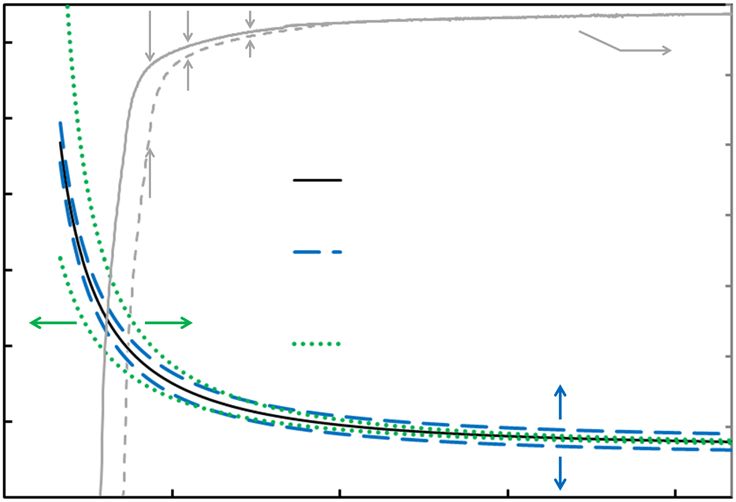
Lapointe et al. Light: Science & Applications (2020)9:64                                                                             Page 4 of 12

 Fig. 2 Calculating the FLIGBS value using the Tauc plot.                  Fig. 3 Sign inversion of the photoinduced refractive index
 Relationship between (αhω)2 and hω for a ZnSe crystal sample before       change in ZnSe. Experimental values of the fs-laser-induced refractive
 (black curve) and after (blue curve) photoinscription (pulse energy of    index change as a function of the propagating wavelength for
 100 nJ with a scan speed of 5mm/s). Their transmission spectra            different laser pulse energies and the theoretical (green dotted) curve
 through the sample with a thickness of d = 1 mm (including Fresnel        from Eq. 4 with dλ1 = 1.26 nm and dN1 = −6.5 × 10⁻³ and using the
 losses) are shown in the inset                                            Sellmeier coefficients from ref. 33

due to the aberration and closer to the surface due to                    approximately 100 meV (dλ1 = 1.23 nm)37. Although this
bubble formation in the oil.                                              demonstrates an FLIBGS, the result is a lower bound since
  The shift in the absorption edge in BaAlBO3F2 and                       the sample is not irradiated over its whole volume.
borosilicate glasses has been observed by two other
groups, but has not been investigated34,35. It is very dif-               Sign inversion of refractive index contrast
ficult to obtain a quantitative measurement of the elec-                     Except for a few demonstrations, such as in ZnSe38,
tronic resonance shift dλ1 from the transmission                          LiNbO3, and Nd:YCa4O(BO3)3, the refractive index
spectrum (inset of Fig. 2). Nevertheless, the absorption                  change is generally negative in crystals5. Therefore, direct
spectrum provides an efficient means to assess the band                    writing of waveguides in crystals is impractical. This can
structure and width of the energy bandgap of optical                      be explained because a positive refractive index change
materials, from which the electronic resonance frequency                  typically requires an increase in the material density,
can be inferred. The optical bandgap Eopt can be expres-                  which is difficult to achieve in crystalline materials due to
sed according to the Tauc law36:                                          the compact structural order of the lattice, in contrast to
                          m                                             vitreous materials with structural disorder and the exis-
    ðαðωÞhωÞ ¼ B hω  Eopt                                          ð5Þ   tence of free space within the network. Figure 3 shows the
                                                                          refractive index contrast Δn for waveguides inscribed in a
where B is a constant depending on the transition                         ZnSe crystal using the same parameters mentioned pre-
probability, α is the absorption coefficient, and is                       viously, with pulse energies from 100 to 195 nJ, as a
calculated using the expression α = −2.303log(T)/d (d is                  function of the propagating wavelength. The results
the thickness of the sample and T is the transmission), ω                 demonstrate a sign inversion of the refractive index
is the incident light angular frequency, Eopt is the width of             change between 550 and 650 nm, depending on the
the bandgap, and m = 1/2 is the refractive index                          energy. To the best of our knowledge, this is the first
characterizing the direct transition process.                             observation of a sign inversion of refractive index contrast
   From the experimental transmission spectrum, (α(ω)                     as a function of the propagating wavelength. Details on
hω)2 can be plotted as a function of hω in eV, as shown in                the refractive index contrast measurement are provided in
Fig. 2. The optical bandgap Eopt is obtained as the inter-                the “Materials and methods” section.
section of the extrapolated linear portion of the curve with                The green dotted curve represents the refractive index
the photon energy hω axis. The bandgap shifts from                        change calculated using Eq. 4 with dλ1 = 1.26 nm and
approximately 2.627–2.620 eV, which corresponds to an                     dN1 = −6.5 × 10⁻³ (chosen to fit the experimental value at
electronic resonance shift of dλ1 = 1.26 nm. As a com-                    700 nm) and using the Sellmeier coefficients from ref. 33.
parison, in typical semiconductors (Eopt ∼10 eV)                          Although the experimental points agree well with the
deformed using the piezospectroscopic effect, the strain-                 theoretical green dotted curve, a significant discrepancy is
induced shift of an electronic resonance may be                           observed at shorter wavelengths, which supports the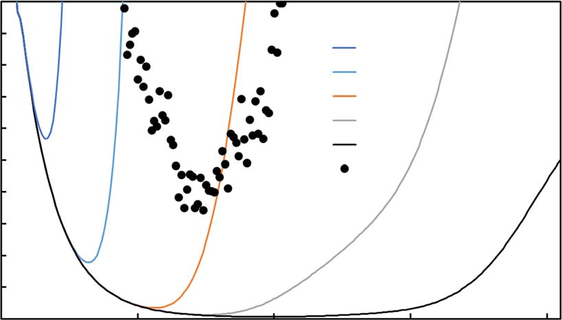
Lapointe et al. Light: Science & Applications (2020)9:64                                                                Page 5 of 12

                                                                      550, 600, and 650 nm. The visibility of the waveguide
                                                                      follows the trend of the refractive index contrast profile
                                                                      shown on the right of Fig. 5 (also see Fig. 3). At 500 and
                                                                      550 nm, the waveguide is clearly seen. At 700 nm, the
                                                                      waveguide is fairly visible. At 600 and 650 nm, the wave-
                                                                      guide is completely invisible to the naked eye and barely
                                                                      visible under the microscope, especially at 600 nm, where
                                                                      it is necessary to fine-tune the microscope focus position
 Fig. 4 Demonstration of light guiding in a ZnSe crystal based on     to make the waveguide barely visible.
 the FLIGBS. Microscope images of two waveguide side views (left)        However, the fs-laser-induced refractive index contrast
 inscribed in ZnSe with pulse energies of 115 and 195 nJ, and their   is not perfectly uniform over the whole inscribed cross
 respective near-field modes imaged at different propagating
                                                                      section, mostly due to the stress induced around the focal
 wavelengths
                                                                      region. This prevents the refractive index contrast from
                                                                      being zero over the full cross-section area of the wave-
                                                                      guide, as shown in the refractive index profile at 600 nm
hypothesis of an underestimation of the band-gap shift                (see Fig. 5, right). The perfect step refractive index
dλ1. The inaccuracy of the empirical Sellmeier coefficients            induced by the fs laser should theoretically enable perfect
from ref. 33 could also contribute to the error, which is             invisibility, a field that has gained much interest in the last
supported by the large difference between the different               decade14–17, including fs-laser-written devices in smart-
values found in the literature39.                                     phone screens, such as temperature sensors40 and on-
   Figure 4 shows the near-field mode profiles of the two               surface refractometric sensors for liquids41, that are
waveguides inscribed in crystalline ZnSe with pulse                   effectively invisible to the naked eye. In these previous
energies of 115 and 195 nJ. With the 115-nJ pulses, the               works40,41, the waveguides are undetectable to the naked
light is weakly confined at 520 nm and not guided at                   eye due to the low laser-induced refractive index change,
633 nm. With the 195-nJ pulses, the light is weakly con-              which limits the waveguide bend radii and thus the
fined at 633 nm and not guided at 1550 nm. At lower                    applications. Therefore, enhancing the invisibility in
wavelengths, the light is strongly confined in the wave-               the visible region while increasing the refractive index
guide at both pulse energies. The trend follows the sign              change at the operating wavelength due to the FLIBGS
inversion of the refractive index contrast. These results             would be of great interest. These invisible waveguide-
are of great interest, since many applications, such as               based devices also have great potential in any see-through
waveguide lasers9, electro-optic modulators10, and fre-               protection screen, such as car windshields, industrial
quency converters11, currently require multi-scan-                    displays, army helmets, and plane dashboards. The use of
depressed cladding structures due to the decrease in the              the multiscan technique or low repetition rates to avoid
refractive index that arises in most crystals5 and a wide             the heating effect42, and methods to minimize aberration
variety of glasses6–8.                                                such as using a spatial light modulator43 or a dual-beam
                                                                      technique44 in order to sharpen the Gaussian intensity
Point of invisible writing                                            profile should help obtain step refractive index inscrip-
  A peculiar phenomenon can be observed in Fig. 3 when                tions. Invisibility at specific wavelengths could enable
the sign of the refractive index change is inverted as a              interesting applications in photonic circuitry and gratings.
function of the wavelength. At a specific wavelength, the                 Note that a sign inversion of the refractive index con-
refractive index contrast becomes zero, which means that              trast and invisibility is not possible via a type III mod-
the laser inscription should be invisible at this wavelength.         ification (damage tracks). The negative refractive index
At Δn = 0, i.e., when n = nirr (cf. Equations 3 and 4), the           contrast produced by voids formed due to microexplo-
propagated light is not affected by the structural mod-               sions remains negative at any optical wavelength. Thus,
ification, which appears to be invisible. Due to the highly            invisibility can only be obtained via a negative refractive
nonlinear effect of dλ1 compared with the effect of dN1,              index change with a type I modification, which has been
invisibility occurs at different wavelengths depending on             achieved in many materials5,45.
the laser inscription parameters. Therefore, the FLIGBS
allows for the direct inscription of invisible structures,            High refractive index contrast allowing compact devices
which does not require invisibility cloaking14–17 to be                 An exponential increase in the refractive index con-
hidden. As a preliminary experimental proof of concept,               trast is observed when approaching the electronic reso-
the left side of Fig. 5 shows the top view of the waveguide           nance at shorter wavelengths (see Fig. 3). This feature is
inscribed in ZnSe using a pulse energy of 170 nJ. The five             very interesting for the fabrication of photonic devices,
pictures were taken with a microscope using filters at 500,            such as splitters, couplers, and ring resonators, with a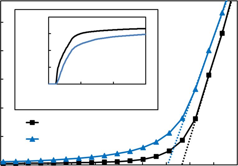
Lapointe et al. Light: Science & Applications (2020)9:64                                                                         Page 6 of 12

                          y

                               z

                                                                                      n
                                                                                                              y

                                                                                      n
                                                                                                              y

                                                                                      n
                                                                                                              y

                                                                                      n
                                                                                                              y

                                                                                      n

                                                                                                              y

 Fig. 5 A waveguide inscribed using a fs laser in a ZnSe crystal becomes nearly invisible near 600 nm. Top views of the waveguide taken with
 a microscope using filters at 500, 550, 600, 650, and 700 nm (left) and their respective refractive index change profiles (right)

submillimeter size. In fact, submillimeter devices are still
nearly impossible to fabricate using fs-laser writing due
to the minimum waveguide bend radius limited by the
refractive index contrast3,18. No one has used wave-
lengths near a material electronic resonance for photo-
nics applications obviously because of the higher
material absorption. A centimeter-long device would be
too lossy to be useful. However, for very compact devi-
ces, the intrinsic material absorption becomes less pro-
blematic. In the following paragraph, we address the
possible benefits of the FLIBGS for the miniaturization
of fs-laser-written photonic circuits.
  To isolate waveguide bend losses, irradiation experi-                   Fig. 6 Exponential increase in the refractive index change in GeS4
                                                                          glass as a function of the propagating wavelength for different
ments were performed on GeS4 glass, which has an
                                                                          laser pulse energies. The gray curve shows the transmission
electronic bandgap lying in the visible region, in which it               spectrum of GeS4 through a 1.22-mm-thick sample (including Fresnel
is easy to photoinscribe type I waveguides46. Figure 6                    losses). For a fixed pulse energy, a significant enhancement of the
shows the refractive index contrast Δn as a function of the               refractive index change is still observed at wavelengths within the
propagating wavelength for waveguides inscribed in GeS4                   highly transparent region
glass using the same parameters mentioned previously,
with pulse energies from 50 to 120 nJ focused 100 μm
beneath the surface using a 50× objective (Edmund Optics                obtained at 500 nm for a pulse energy of 90 nJ. Note that
LWD 0.55 NA). The exponential increase in the refractive                this value of 1.7 × 10⁻² is, to the best of our knowledge,
index contrast is clearly observed at short wavelengths.                the highest fs-laser-induced smooth positive type I
Positive refractive index changes up to ~1.7 × 10⁻² are                 refractive index change observed in any chalcogenide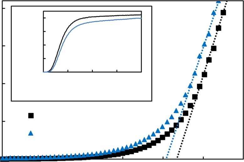
Lapointe et al. Light: Science & Applications (2020)9:64                                                                    Page 7 of 12

                                                                    a

 Fig. 7 Top-view microscope image of an S-bend waveguide (with
 R = 363 μm) photoinscribed in GeS4 glass and (inset) its near-
 field mode profile at 520 nm with a width of 9.5 μm. See the
 dynamics of the guided light in the Supplementary Movie            b

glass waveguide. The gray curve shows the transmission
spectrum of the GeS4 glass through a 1.22-mm-thick
sample (including Fresnel losses). For a fixed pulse energy,
it is interesting to see that a significant enhancement of
the refractive index change is still obtained at wavelengths
within the highly transparent region. This extends the
range of applications of FLIBGS-based devices.
   To ensure a smooth inscription of the tightly curved
waveguides, the scan speed was reduced to 1 mm/s. Then,
20-nJ pulses were focused 100 μm beneath the surface               Fig. 8 Optical losses as a function of the bend radius. a
using a 100× oil immersion objective (1.25 NA). To isolate         Waveguide bend loss and b effective loss (bend loss plus material
the curvature loss, several S-bend waveguides were writ-           absorption) at 520, 633, and 1550nm as a function of the radius
ten in a 6-mm-long GeS4 sample, as shown in Fig. 7. Six            curvature of an S bend photoinscribed in GeS4 glass. The solid curves
                                                                   are the theoretical curves obtained from Eq. 6. Despite the high
S-bend waveguides with a fixed lateral displacement of
                                                                   material absorption loss, it is advantageous to use smaller
200 μm with lengths L ranging from 0.5 mm (with a radius           wavelengths for very small bend radii (e.g., 480-nm solid curve)
curvature R of 0.363 mm) to 6 mm (R = 45.05 mm) were
written.
   The S-bend waveguides were characterized using 520-,           material with a bandgap far from this wavelength, such as
633-, and 1550-nm laser sources. The light injection was          standard glasses (e.g., soda lime, borosilicate, and fused
performed by butt-coupling with a single-mode fiber.               silica). In addition to the high refractive index contrast
Simply by measuring the additional loss relative to a             obtained due to the FLIBGS, the smooth type I-positive
straight waveguide written under the same conditions, the         refractive index change may have an important impact on
additional loss from each S bend can be isolated. The             the guiding property of waveguides with submillimeter
bend loss in dB/mm is obtained by dividing this additional        bend radii. In fact, a high refractive index contrast can be
loss over the S-bend waveguide length. The results are            achieved with mixes of positive and negative refractive
plotted in Fig. 8a. At 1550 nm, the results are in agree-         index changes or with type III (microexplosion or damage
ment with prior results from the literature3,18. For a radius     tracks) waveguides. However, the high asymmetry or
curvature of 5 mm, the loss is less than 0.5 dB/mm at             roughness typically obtained from these methods induces
520 nm, while it is over four times higher at 1550 nm. For        additional losses in waveguide bends.
a radius curvature of 1.3 mm, the signal is completely lost          The experimental values can be compared with the
at 1550 nm, while the loss is less than 6 dB/mm at 520 nm.        theoretical formula of the waveguide bend loss LB (dB/
For a radius of curvature of 363 μm, guiding occurs only          mm)47:
with the 520-nm light, with a bend loss of 17 ± 2 dB/mm,
which seems promising for sub-millimeter-size devices,                                 1=2
                                                                          LB ¼ 2:171π1=2          V4
                                                                                                  2       1=2
                                                                                 ðρRÞ       ðV þ1Þ ðV 1Þ
considering that 520 nm is not the optimized wavelength.                     h                                i                    ð6Þ
                                                                               ðV 1Þ2     4RðV 1Þ3 n2irr n2
Note that we have not been able to guide 520-nm light                   ´ exp V þ1  3ρV 2              2n2
                                                                                                          irr
through waveguides with submillimeter bend radii in a
Lapointe et al. Light: Science & Applications (2020)9:64                                                                     Page 8 of 12

where ρ is the waveguide core radius and V is the
                                                                   a
waveguide parameter given by:

          2πρ  2        1=2
    V ¼        nirr  n2                                   ð7Þ
           λ

  The theoretical bend loss curves for 520, 633, and
1550 nm are plotted in Fig. 8a (solid curves). The differ-
ences between the experimental values and the theoretical
curves can be explained by the perturbation at the tran-
sition point (halfway point of the S bend) where the curve
changes the direction of its rotation47, which is not taken
into account in Eq. 6, and the fact that defects and
waveguide roughness have more significant effects for               b
curved segments. Moreover, Eq. 6 is an approximation for
perfectly symmetrical single-mode waveguides, which is
not exactly the case in our experiment. As shown in the
inset of Fig. 7, the mode profile is slightly elongated, and
few modes appear at smaller wavelengths. The refractive
index values of the GeS4 glass were obtained using an
interpolation from five measurements (n = 2.153, 2.109,
2.058, 2.044, and 2.039 at wavelengths λ = 532, 633, 972,
1303, and 1538 nm, respectively) using a Metricon 2010/
M prism coupler.
  However, the most important parameter is the total loss
                                                                  Fig. 9 Effective loss as a function of the wavelength. a Theoretical
of such curved waveguide-based devices. The mode mis-             effective loss (bend loss plus material absorption) as a function of the
match and Fresnel losses (at the input and output) can be         propagating wavelength for various waveguide bend radii
easily reduced to less than 1 dB47 and remain the same for        photoinscribed in GeS4 glass. b Zoom-in of the microbend region. The
any S-bend size; therefore, they are not taken into account       experimental points (black circles) include the Fresnel, mode
                                                                  mismatch, and misalignment losses
in the following loss estimation. At wavelengths far from
the resonances, the propagation loss in straight wave-
guides can be as low as 0.01 dB/mm1. This waveguide
propagation loss is negligible compared with the bend loss       These relatively low losses are due to the fact that at 520
and material absorption at wavelengths near electronic           and 633 nm, the material absorption is still low, while the
resonance and even more negligible for compact devices,          refractive index is significantly increased (see Fig. 6) due
which is the subject of this study. Figure 8b shows the sum      to the FLIBGS.
of the two main optical losses (bend loss and material             Despite the differences between the experimental points
absorption), which will be referred to as the “effective         and the theoretical curves in Fig. 8b, both clearly show the
loss”, for several wavelengths as a function of the wave-        same trend. Therefore, the theoretical calculation can be
guide bend radius. The absorption spectrum of the GeS4           used to provide an optimized wavelength for a specific
glass was measured using an Agilent Cary 5000                    bend radius required for a specific application. The curves
UV–vis–NIR system. Despite the higher absorption near            in Fig. 9 show the theoretical effective loss as a function of
electronic resonance, the experimental values and the            the wavelength for different waveguide bend radii pho-
theoretical curves in Fig. 8b clearly show the advantage of      toinscribed in GeS4 glass. Optimized wavelengths of 895,
using wavelengths near resonance for tightly curved              620, 545, 525, 505, 480, and 467 nm are obtained for bend
waveguides. For example, from the experimental mea-              radii of 5, 2, 1.3, 1, 0.75, 0.5, and 0.375 mm, respectively.
surements, a 1-mm-long optical splitter with a lateral           Moreover, as shown in Fig. 9a, low-loss compact devices
displacement of the outputs of 400 μm, which is made of          made of waveguides with a bend radius of 5 mm should be
two S bends, as shown in Fig. 7, with a waveguide bend           achievable over a bandwidth of ∼600 nm (from ∼550 to
radius of 1.3 mm, exhibits an effective loss of 6.1 dB at        ∼1150 nm).
520 nm, while the signal is completely lost at 1550 nm. For        Figure 9b shows the experimental effective loss mea-
a 1.6-mm-long splitter with a lateral displacement of the        surement (black circles) using an optical spectrum ana-
outputs of 250 μm, with a waveguide bend radius of               lyzer (Yokogawa AQ6373B) from a white-light source
5 mm, the experimental effective loss is 2.16 dB at 633 nm.      (Koheras SuperK Power supercontinuum source)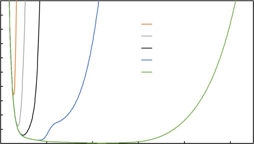
Lapointe et al. Light: Science & Applications (2020)9:64                                                                Page 9 of 12

launched in an S-bend waveguide (as shown in Fig. 7) with             of GeS4 (2.1089 at 633 nm) makes deeper writing feasible,
a bend radius of 1.3 mm. While this method of analysis is             which probably contributes to the larger calculated band-
not precise enough to obtain a reliable measurement of                gap shift compared with the shift for ZnSe. Unfortunately,
the losses (it also includes Fresnel, mode mismatch, and              since no Sellmeier coefficients were found in the literature
misalignment losses), it provides a relative value of losses          for GeS4 glass, the theoretical curve of the refractive index
as a function of the wavelength. Therefore, the experi-               contrast as a function of the wavelength could not be
mental values show the real optimized wavelength                      plotted in Fig. 6. As a comparison, a band-gap shift of
(524 nm), which is 21 nm shorter than the theoretical                 approximately 0.06 eV (dλ1 ∼10 nm) was observed after
wavelength. This can be explained by any waveguide                    illuminating a GeS2.33 film for 4 h using a 400-W high-
fluctuation, roughness, or defects caused by laser                     pressure Hg lamp48. One may notice a surprising increase
inscription power fluctuations, scratches on the surface,              in the absorption in the full spectrum for the irradiated
motor vibrations, or material imperfection, which results             samples compared with that of the pristine samples (see
in a lower effective bend radius. Note that the Fresnel and           the inset in Figs. 2 and 10). This is due to the light scat-
mode mismatch losses are wavelength-dependent but                     tered from the non-uniformly inscribed sample, which is
should not significantly affect the value of the obtained              not detected by the Cary detector. To ensure that this
optimized wavelength.                                                 scattered light did not affect the band-gap shift calcula-
   As shown in Fig. 9b, for very tight bends, the wavelength          tion, a few measurements were performed using a
is more critical. In the case where the application requires          detector close to the sample to measure all of the scat-
the tightest bend, the use of the Tauc law (see Eq. 5 and             tered light, which provided the same results but with a
Fig. 2) seems to be a practical way to obtain an efficient             higher experimental error. These measurements also
and reliable wavelength (or a good material choice for a              ensured that the laser inscription did not induce sig-
fixed wavelength of interest). For GeS4 glass, a bandgap of            nificant absorption loss, which was also demonstrated by
464 nm (2.67 eV) is obtained. At this wavelength, the                 Tong et al.49.
losses (1.13 dB/100 μm) are mostly due to material
absorption down to a bend radius of 430 μm. For a bend                Discussion
radius of 375 μm, an effective loss of 1.2 dB/100 μm is                 The origin of the FLIBGS is complex and depends on
calculated.                                                           the irradiated material. In glasses, the network consists of
   As shown in Fig. 10, to obtain a lower bound of the                a disordered arrangement of structural units such as tet-
FLIBGS in GeS4 glass, the same procedure using the Tauc               rahedra (e.g., [SiO4] or [GeS4] in silica or germanium
law was executed (see section “FLIBGS theory and                      sulfide glasses, respectively), with the existence of free
experiment”). The sample was irradiated from a depth of               space and local defects. This network therefore provides
60–660 μm over the sample with a thickness of d =                     favorable conditions for material modifications under an
1.22 mm. The bandgap shifts from approximately                        external stimulus such as fs-laser pulses. On the other
2.67–2.655 eV, which corresponds to an electronic reso-               hand, in a crystalline material (e.g., ZnSe), the structure is
nance shift of dλ1 = 2.62 nm. The lower refractive index              well organized without free space and has much fewer
                                                                      defects than glasses. This structure then has fewer degrees
                                                                      of freedom for photoinduced modifications. Nevertheless,
                                                                      if the amplitude of photosensitivity that distinguishes
                                                                      these two materials is not considered, the nature of
                                                                      the photoinduced changes is similar. Most of the time, the
                                                                      photoinduced changes are a combination of two or more
                                                                      of the following effects: the formation of color centers,
                                                                      the migration of species, the modification of structural
                                                                      units (bond or bonding angle that breaks or changes), and
                                                                      even crystallization or amorphization1,6,7. These phe-
                                                                      nomena then result in a highly localized contraction/
                                                                      dilatation of the structure (i.e., a local density increase or
                                                                      decrease) locally altering the electron density and thus the
                                                                      energy required to cross the bandgap. Although the origin
 Fig. 10 Calculating the FLIGBS value using the Tauc plot.            of these phenomena remains complex, the phenomena
 Relationship between (αhω)2 and hω for a GeS4 glass sample before    are generally associated with a band-gap shift (also called
 (black squares) and after (blue triangles) photoinscription. Their   a transmission or absorption edge shift, photodarkening
 transmission spectra through the sample with a thickness of
 d = 1.22 mm (including Fresnel losses) are shown in the inset
                                                                      or photobleaching, or an electronic resonance shift). This
                                                                      is also in agreement with previously reported band-gap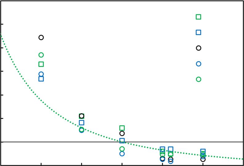
Lapointe et al. Light: Science & Applications (2020)9:64                                                                         Page 10 of 12

increases due to a decrease in lattice spacing in a semi-        supported by the disordered refractive index profile
conductor under hydrostatic pressure50 and using the             shown in Fig. 5.
piezospectroscopic effect37. Moreover, an absorption edge          Finally, we have demonstrated an exponential increase
shift has been observed in chalcogenide glasses after            in the photoinduced refractive index contrast for propa-
illumination whose energy equals or exceeds the band-gap         gating wavelengths approaching electronic resonances.
energy51. Light-induced creation of dangling bonds               Unveiled by the Kramers–Kronig relations, this increase is
(immobilized free radicals) has been considered to be the        caused by a FLIBGS in the irradiated region of transparent
origin of the phenomenon52,53. Recently, the creation of         materials. For each material and laser, several writing
high-density dangling bonds after pulsed-laser excitation        parameters must be tuned to form a strong waveguide (far
has been observed in hydrogenated amorphous sili-                from resonance). In this paper, strong waveguides were
con54,55, which could partly explain the FLIGBS. Several         not the scope of the work, and only the pulse energy was
models have been proposed to describe the mechanisms             tuned to obtain decent waveguides to study the effects of
involved in the creation of dangling bonds under illumi-         an FLIBGS. Therefore, it would be of great interest to
nation with energy exceeding the band-gap energy, but            study the effects of an FLIBGS on known strong recipes
this issue is still controversial51,56. Moreover, from the       and observe how the FLIBGS can push the limits of
illumination of chalcogenide glasses under near-band-gap         refractive index contrast and the waveguide bend radius.
light (e.g., a Hg lamp), the evidence suggests that the          Exploring FLIBGS applications opens up great research
observed band-gap shift is due to an increase in structural      opportunities for the entire spectral range in photonics,
intermediate-range disorder (randomness)48,57,58. This           since electronic band gaps lying in the ultraviolet, visible,
structural randomness may broaden the resonance fre-             and infrared regions can be found in different materials.
quency band. Similarly, the naturally random amorphous
state of a material generally has a lower band-gap energy        Materials and methods
than its crystalline state59,60. This latter explanation may     Refractive index modification measurement
have an important impact on the band-gap shift in crys-            To measure the photoinduced refractive index mod-
tals, in which the structure becomes locally disordered          ifications, the structures were examined using a bright-
under fs-laser illumination. Finally, despite these expla-       field microscope (Olympus IX71) and a camera equipped
nation attempts, the origins of the band-gap shift are still     with a bidimensional Hartmann grating (Phasics SID4-
unclear61.                                                       Bio). The camera system acts as a wavefront analyzer that
   One can note the unusual behavior of the refractive           uses lateral shearing interferometry (QWLSI) to generate
index contrast for different laser pulse energies at the         a quantitative phase image of transparent objects62. This
same wavelength in Figs. 3 and 6. In Fig. 6, at low energy,      methodology, described in detail in ref. 63, was carried out
it is observed that the refractive index contrast increases      to recover the refractive index change (Δn) of the wave-
with increasing pulse energy, whereas at higher energy,          guides from the phase image. Accordingly, Δn measure-
the refractive index contrast decreases. This behavior was       ments were considered to be exact within a 2% error
reported in a previous work46 and explained by a                 margin or better. Since the Phasics camera operates in the
saturation point of the refractive index change that occurs      visible range, ZnSe crystal and GeS4 glass, both of which
when the size of the waveguides surpasses the dimension          have electronic bandgaps in the visible range, are excellent
of the fs-laser-induced plasma during the inscription. In        materials for the experiment.
the experiments presented in Fig. 6, the waveguide sizes
surpassing the plasma size are denoted by squares (circle        Samples
otherwise). The behavior follows the previous observa-             Germanium sulfide (GeS4) glass samples were fabricated
tion46, and the maximum refractive index contrast occurs         in-house following conventional melting–quenching tech-
for the highest energy pulse without the waveguide               niques46. The polycrystalline ZnSe sample was obtained
exceeding the plasma size, i.e., at 90 nJ. As shown in Fig. 3,   from a commercial supplier (Mellers Optic).
the same trend is observed in the ZnSe crystal, where the
                                                                 Acknowledgements
maximum refractive index contrast is obtained at 130 nJ.         We acknowledge funding from the Natural Sciences and Engineering Research
The refractive index change is most negative in the red          Council of Canada (NSERC) (IRCPJ469414-13), Canada Foundation for
part of the spectrum and most positive in the blue part.         Innovation (CFI) (33240 and 37422), Canada Excellence Research Chair (CERC in
                                                                 Photonic Innovations), FRQNT strategic cluster program (2018-RS-203345),
Similarly, at 170 nJ, the refractive index change is less        Quebec Ministry of Economy and Innovation (PSRv2-352), and Canada First
negative in the red part of the spectrum and less positive       Research Excellence Fund (Sentinel North).
in the blue part. However, there is no such clear trend
near the inversion of the sign of the refractive index           Author contributions
                                                                 J.L. conceived the idea, designed the experiment, and performed the optical
change. This is probably due to the nonlinear nature of          measurements. J.L., J.-P.B., and A.D. performed the theoretical simulations. Y.L.
the refractive index change mechanisms, which is                 and Y.M. fabricated the GeS4 samples. J.L. wrote the paper with contributions
Lapointe et al. Light: Science & Applications (2020)9:64 Page 11 of 12
from J.-P.B., Y.L. V.F., and R.V. All of the authors analyzed the results and 26. Davis, K. M. et al. Writing waveguides in glass with a femtosecond laser. Opt.
commented on the paper. Lett. 21, 1729–1731 (1996).
27. Hirao, K. & Miura, K. Writing waveguides and gratings in silica and related
Conflict of interest materials by a femtosecond laser. J. Noncryst. Solids 239, 91–95 (1998).
The authors declare that they have no conflict of interest. 28. Mao, S. S. et al. Dynamics of femtosecond laser interactions with dielectrics.
Appl. Phys. A 79, 1695–1709 (2004).
Supplementary information is available for this paper at https://doi.org/ 29. Streltsov, A. M. & Borrelli, N. F. Study of femtosecond-laser-written waveguides
10.1038/s41377-020-0298-8. in glasses. J. Optical Soc. Am. B 19, 2496–2504 (2002).
30. Lucarini, V. et al. Kramers-Kronig Relations in Optical Materials Research.
(Springer, Berlin, 2005).
Received: 7 November 2019 Revised: 20 February 2020 Accepted: 19 March 31. Korff, S. A. & Breit, G. Optical dispersion. Rev. Mod. Phys. 4, 471–503 (1932).
2020 32. Ghosh, G. Sellmeier coefficients and dispersion of thermo-optic coefficients for
some optical glasses. Appl. Opt. 36, 1540–1546 (1997).
33. Marple, D. T. F. Refractive index of ZnSe, ZnTe, and CdTe. J. Appl. Phys. 35,
539–542 (1964).
References 34. Lin, G. et al. Different refractive index change behavior in borosilicate glasses
1. Gattass, R. R. & Mazur, E. Femtosecond laser micromachining in transparent induced by 1 kHz and 250 kHz femtosecond lasers. Optical Mater. Express 1,
materials. Nat. Photonics 2, 219–225 (2008). 724–731 (2011).
2. Malinauskas, M. et al. Ultrafast laser processing of materials: from science to 35. Du, X. et al. Femtosecond laser induced space-selective precipitation of a
industry. Light 5, e16133 (2016). deep-ultraviolet nonlinear BaAlBO3F2 crystal in glass. J. Noncryst. Solids 420,
3. Eaton, S. M. et al. High refractive index contrast in fused silica waveguides by 17–20 (2015).
tightly focused, high-repetition rate femtosecond laser. J. Noncryst. Solids 357, 36. Tauc, J. Optical properties and electronic structure of amorphous Ge and Si.
2387–2391 (2011). Mater. Res. Bull. 3, 37–46 (1968).
4. Arriola, A. et al. Low bend loss waveguides enable compact, efficient 3D 37. Akimov, A. V. et al. Ultrafast band-gap shift induced by a strain pulse in
photonic chips. Opt. Express 21, 2978–2986 (2013). semiconductor heterostructures. Phys. Rev. Lett. 97, 037401 (2006).
5. Chen, F. & De Aldana, J. R. V. Optical waveguides in crystalline dielectric 38. Macdonald, J. R. et al. Ultrafast laser inscription of near-infrared waveguides in
materials produced by femtosecond-laser micromachining. Laser Photonics polycrystalline ZnSe. Opt. Lett. 35, 4036–4038 (2010).
Rev. 8, 251–275 (2014). 39. Tatian, B. Fitting refractive-index data with the Sellmeier dispersion formula.
6. Tan, D. Z. et al. Femtosecond laser induced phenomena in transparent solid Appl. Opt. 23, 4477–4485 (1984).
materials: fundamentals and applications. Prog. Mater. Sci. 76, 154–228 (2016). 40. Lapointe, J. et al. Making smart phones smarter with photonics. Opt. Express
7. Fernandez, T. T. et al. Bespoke photonic devices using ultrafast laser driven ion 22, 15473–15483 (2014).
migration in glasses. Prog. Mater. Sci. 94, 68–113 (2018). 41. Lapointe, J. et al. Toward the integration of optical sensors in smart-
8. Gross, S. et al. Ultrafast laser inscription in soft glasses: a comparative study of phone screens using femtosecond laser writing. Opt. Lett. 40, 5654–5657
athermal and thermal processing regimes for guided wave optics. Int. J. Appl. (2015).
Glass Sci. 3, 332–348 (2012). 42. Eaton, S. M. et al. Heat accumulation effects in femtosecond laser-written
9. Lapointe, J. et al. Fabrication of ultrafast laser written low-loss waveguides in waveguides with variable repetition rate. Opt. Lett. 13, 4708–4716 (2005).
flexible As2S3 chalcogenide glass tape. Opt. Lett. 41, 203–206 (2016). 43. Jesacher, A. et al. Adaptive optics for direct laser writing with plasma emission
10. Okhrimchuk, A. G. et al. Depressed cladding, buried waveguide laser formed in aberration sensing. Opt. Express 18, 656–661 (2010).
a YAG: Nd3+ crystal by femtosecond laser writing. Opt. Lett. 30, 2248–2250 44. Lapointe, J. & Kashyap, R. A simple technique to overcome self-focusing,
(2005). filamentation, supercontinuum generation, aberrations, depth dependence
11. Liao, Y. et al. Electro-optic integration of embedded electrodes and wave- and waveguide interface roughness using fs laser processing. Sci. Rep. 7, 499
guides in LiNbO3 using a femtosecond laser. Opt. Lett. 33, 2281–2283 (2008). (2017).
12. Burghoff, J. et al. Efficient frequency doubling in femtosecond laser-written 45. Bérubé, J. P. et al. Femtosecond laser inscription of depressed cladding
waveguides in lithium niobate. Appl. Phys. Lett. 89, 081108 (2006). single-mode mid-infrared waveguides in sapphire. Opt. Lett. 44, 37–40
13. Poumellec, B. et al. Modification thresholds in femtosecond laser processing of (2019).
pure silica: review of dependencies on laser parameters [Invited]. Optical Mater. 46. Bérubé, J. P. et al. Tailoring the refractive index of Ge-S based glass for 3D
Express 1, 766–782 (2011). embedded waveguides operating in the mid-IR region. Opt. Express 22,
14. Zhang, B. L. et al. Macroscopic invisibility cloak for visible light. Phys. Rev. Lett. 26103–26116 (2014).
106, 033901 (2011). 47. Snyder, A. W. & Love, J. Optical Waveguide Theory. (Springer Science & Business
15. Cortés, L. R. et al. Full-field broadband invisibility through reversible wave Media, New York, 1983).
frequency-spectrum control. Optica 5, 779–786 (2018). 48. Shimizu, T. et al. Photo-induced ESR and optical absorption edge shift in
16. Pendry, J. B., Schurig, D. & Smith, D. R. Controlling electromagnetic fields. amorphous Ge-S films. Solid State Commun. 27, 223–227 (1978).
Science 312, 1780–1782 (2006). 49. Tong, L. et al. Optical loss measurements in femtosecond laser written
17. Leonhardt, U. Optical conformal mapping. Science 312, 1777–1780 (2006). waveguides in glass. Opt. Commun. 259, 626–630 (2006).
18. Charles, N. et al. Design of optically path-length-matched, three-dimensional 50. Neuberger, M. Handbook of Electronic Materials: Volume 5: Group IV Semi-
photonic circuits comprising uniquely routed waveguides. Appl. Opt. 51, conducting Materials. (Springer Science & Business Media, New York, 2012).
6489–6497 (2012). 51. Singh, J. & Shimakawa, K. Advances in Amorphous Semiconductors. (CRC Press,
19. Levinshtein, M., Rumyantsev, S. & Shur, M. S. Handbook Series on Semiconductor London, 2003).
Parameters (Singapore New Jersey: World Scientific, 1996). 52. Hirabayashi, I., Morigaki, K. & Nitta, S. New evidence for defect creation by high
20. Beresna, M., Gecevičius, M. & Kazansky, P. G. Ultrafast laser direct writing and optical excitation in glow discharge amorphous silicon. Jpn. J. Appl. Phys. 19,
nanostructuring in transparent materials. Adv. Opt. Photonics 6, 293–339 (2014). L357 (1980).
21. Sundaram, S. K. & Mazur, E. Inducing and probing non-thermal transitions in 53. Dersch, H., Stuke, J. & Beichler, J. Light‐induced dangling bonds in hydro-
semiconductors using femtosecond laser pulses. Nat. Mater. 1, 217–224 (2002). genated amorphous silicon. Appl. Phys. Lett. 38, 456–458 (1981).
22. Chan, J. W. et al. Structural changes in fused silica after exposure to focused 54. Ogihara, C. et al. Lifetime and intensity of photoluminescence after light
femtosecond laser pulses. Opt. Lett. 26, 1726–1728 (2001). induced creation of dangling bonds in a-Si: H. J. Noncryst. Solids 299–302,
23. Juodkazis, S. et al. Laser-induced microexplosion confined in the bulk of a 637–641 (2002).
sapphire crystal: evidence of multimegabar pressures. Phys. Rev. Lett. 96, 55. Morigaki, K. et al. Light-induced defect creation under pulsed subbandgap
166101 (2006). illumination in hydrogenated amorphous silicon. Philos. Mag. Lett. 83, 341–349
24. Sakakura, M. et al. Observation of pressure wave generated by focusing a (2003).
femtosecond laser pulse inside a glass. Opt. Express 15, 5674–5686 (2007). 56. Morigaki, K. Physics of Amorphous Semiconductors. (World Scientific Press,
25. Lucarini, V. et al. Kramers–Kronig Relations in Optical Materials Research London, 1999).
(Springer, Berlin, 2005).Lapointe et al. Light: Science & Applications (2020)9:64 Page 12 of 12
57. Pfeiffer, G., Paesler, M. A. & Agarwal, S. C. Reversible photodarkening of 61. Kasap, S. & Capper, P. Springer Handbook of Electronic and Photonic Materials.
amorphous arsenic chalcogens. J. Noncryst. Solids 130, 111–143 (1991). (Springer, Cham, 2017).
58. Street, R. A. Non-radiative recombination in chalcogenide glasses. Solid State 62. Roberts, A. et al. Refractive-index profiling of optical fibers with axial symmetry
Commun. 24, 363–365 (1977). by use of quantitative phase microscopy. Opt. Lett. 27, 2061–2063 (2002).
59. Feltz, A. Amorphous Inorganic Materials and Glasses. (VCH, Weinheim, 1993). 63. Bélanger, E. et al. Comparative study of quantitative phase imaging techni-
60. Stuke, J. Review of optical and electrical properties of amorphous semi- ques for refractometry of optical waveguides. Opt. Express 26, 17498–17510
conductors. J. Noncryst. Solids 4, 1–26 (1970). (2018).You can also read