Recent advances in ultraviolet nanophotonics: from plasmonics and metamaterials to metasurfaces - De Gruyter
←
→
Page content transcription
If your browser does not render page correctly, please read the page content below
Nanophotonics 2021; 10(9): 2283–2308

Review

Dong Zhao, Zhelin Lin, Wenqi Zhu, Henri J. Lezec, Ting Xu, Amit Agrawal, Cheng Zhang*
and Kun Huang*

Recent advances in ultraviolet nanophotonics:
from plasmonics and metamaterials to
metasurfaces
https://doi.org/10.1515/nanoph-2021-0083                                    techniques, followed by representative device applications
Received February 28, 2021; accepted April 21, 2021;                        across various interdisciplinary areas such as imaging,
published online May 24, 2021                                               sensing and spectroscopy. We conclude this review by
                                                                            elaborating on future opportunities and challenges for ul-
Abstract: Nanophotonic devices, composed of metals,
                                                                            traviolet nanophotonic devices.
dielectrics, or semiconductors, enable precise and high-
spatial-resolution manipulation of electromagnetic waves                    Keywords: metamaterials; metasurfaces; nanophotonics;
by leveraging diverse light–matter interaction mechanisms                   plasmonics; ultraviolet light.
at subwavelength length scales. Their compact size,
light weight, versatile functionality and unprecedented
performance are rapidly revolutionizing how optical                         1 Introduction
devices and systems are constructed across the infrared,
visible, and ultraviolet spectra. Here, we review recent                    “Ultraviolet” means “beyond violet”, where violet refers
advances and future opportunities of nanophotonic                           to the color of visible spectrum with the highest photon
elements operating in the ultraviolet spectral region, which                energy. Ultraviolet (UV) radiation was discovered by
include plasmonic devices, optical metamaterials, and                       German physicist Johann Wilhelm Ritter in the year 1801
optical metasurfaces. We discuss their working principles,                  [1]. Ritter observed that invisible rays beyond the violet
material platforms, fabrication, and characterization                       end of the visible spectrum had an even stronger
                                                                            interaction with silver chloride-soaked papers than the
Dong Zhao and Zhelin Lin contributed equally to this work.                  violet light, and therefore called these rays “deoxidiz-
                                                                            ing rays” to emphasize their chemical reactivity.
*Corresponding authors: Cheng Zhang, School of Optical and
                                                                            Nowadays, UV radiation typically refers to electro-
Electronic Information & Wuhan National Laboratory for
Optoelectronics, Huazhong University of Science and Technology,
                                                                            magnetic waves with free-space wavelengths between
Wuhan, Hubei 430074, China, E-mail: cheng.zhang@hust.edu.cn;                10 and 380 nm, and can be further divided into five sub-
and Kun Huang, Department of Optics and Optical Engineering,                bands (Figure 1a), which are the near-UV range [2] (UV-A;
University of Science and Technology of China, Hefei, Anhui 230026,         free-space wavelength range: 315 nm ≤ λ0 ≤ 380 nm;
China, E-mail: huangk17@ustc.edu.cn
                                                                            photon energy range: 3.26 eV ≤ E0 ≤ 3.94 eV), the mid-UV
Dong Zhao, Department of Optics and Optical Engineering, University
of Science and Technology of China, Hefei, Anhui 230026, China              range (UV-B; 280 nm ≤ λ0 ≤ 315 nm; 3.94 eV ≤ E0 ≤ 4.43 eV),
Zhelin Lin, School of Optical and Electronic Information & Wuhan            the deep-UV range (longer wavelength portion of
National Laboratory for Optoelectronics, Huazhong University of             UV-C; 190 nm ≤ λ0 ≤ 280 nm; 4.43 eV ≤ E0 ≤ 6.53 eV), the
Science and Technology, Wuhan, Hubei 430074, China                          vacuum-UV range (shorter wavelength portion of
Wenqi Zhu and Amit Agrawal, Physical Measurement Laboratory,
                                                                            UV-C; 100 nm ≤ λ0 ≤ 190 nm; 6.53 eV ≤ E0 ≤ 12.40 eV),
National Institute of Standards and Technology, Gaithersburg, MD
20877, USA; and Maryland NanoCenter, University of Maryland,                and the extreme-UV range (10 nm ≤ λ0 ≤ 100 nm;
College Park, MD 20742, USA                                                 12.40 eV ≤ E0 ≤ 123.98 eV). UV radiation can be produced
Henri J. Lezec, Physical Measurement Laboratory, National Institute of      by both natural objects such as sun, or artificial sources
Standards and Technology, Gaithersburg, MD 20877, USA
                                                                            such as gas-discharge lamps, lasers (e.g., argon-ion
Ting Xu, National Laboratory of Solid State Microstructures & College
of Engineering and Applied Sciences and Collaborative Innovation
                                                                            laser, helium–cadmium laser, argon-fluoride excimer
Center of Advanced Microstructures, Nanjing University, Nanjing,            laser etc.), light emitting diodes [3–5], nonlinear mate-
Jiangsu 210093, China                                                       rials [6–11], plasmas [12], and synchrotron [13].
  Open Access. © 2021 Dong Zhao et al., published by De Gruyter.         This work is licensed under the Creative Commons Attribution 4.0 International
License.
2284           D. Zhao et al.: Recent advances in ultraviolet nanophotonics

Figure 1: (a) Electromagnetic spectrum for the UV range and the constituent five sub-bands. (b) Representative applications of UV radiation.

     UV light plays an irreplaceable role in both funda-                expensive, and require complex processing. For instance,
mental research and practical applications, ranging from                high-refractive-index materials are preferred for various
spectroscopy, imaging, microscopy, quantum optics,                      optoelectronic applications including antireflection
and time keeping, to lithography, light therapy, micro-                 coatings, filters, waveguides, etc. Unfortunately, many
machining, and sterilization (Figure 1b). For example,                  high-refractive-index materials are characterized by a
circular dichroism (CD) spectroscopy using near-UV light                relatively narrow bandgap, resulting in a high absorption
is widely used for characterizing the secondary structures              of UV light. Consequently, UV optical elements are limited
of proteins [14], while CD spectroscopy using deep-UV light             in functionality, diversity, operational bandwidth, and
is largely employed during the exploration and quality                  manufacturability, in comparison to their near-IR and
evaluation of chiral pharmaceuticals [15, 16]. Similarly, UV            visible counterparts. While exploring new UV materials
spectrophotometry is widely used for nucleic acid quanti-               and associated manufacturing techniques to overcome
zation [17, 18]. Also, UV light source has long been an                 the aforementioned limitations, researchers are also
essential component in different generations of lithog-                 exploiting new strategies that are based on nanophotonic
raphy systems, whose resolution depends critically on the               technology, including those based on plasmonics,
wavelength of the employed UV source [19, 20]. Unlike                   metamaterial, and metasurface concepts. Contrary to
electromagnetic radiation at lower frequencies, UV radia-               conventional optical elements which reflect, refract, or
tion can cause ionization and breakage of chemical bonds.               diffract a light beam with their spatially varying shapes,
Consequently, UV light is widely used for air purification,              nanophotonic devices modulate various parameters of an
waste-water treatment, micro-organism, and virus inacti-                electromagnetic wave (e.g., amplitude, phase or polariza-
vation, etc. [21, 22].                                                  tion state) by engineering their constituent subwavelength
     So far, manipulation of UV light largely relies on                 unit cells [23–26]. These nanoscale building blocks can
conventional refractive or reflective optical elements. In              be judiciously designed such that the entire device either
contrast to diverse optical materials that are low loss in              exhibits an electromagnetic response rarely found in na-
the near-infrared (near-IR) and visible spectra, suitable               ture, or provides similar or even superior functionality
materials for the UV region (specially for the deep-UV and              compared to its conventional bulk-optic counterpart,
even shorter wavelength regions) are relatively limited,                but with a tremendously reduced size. Consequently,
D. Zhao et al.: Recent advances in ultraviolet nanophotonics     2285

nanophotonic technology holds great potential in creating       shown in Figure 2b) [34]. Other metals such as gallium (Ga),
high-performance optoelectronic systems with novel              indium (In), tin (Sn), titanium (Ti), lead (Pb), and bismuth
functionality, low loss, and compact footprint [27–29].         (Bi) have also been explored as alternate UV plasmonic
     In this review, we summarize previous achievements of      materials as their permittivity also exhibits a negative real
UV nanophotonics technology and discuss its challenges          part in the UV [35]. Recently, silicon (Si), as a representative
as well as opportunities. We will first elaborate on UV          semiconductor material, has been found to support SPPs
plasmonic devices by explaining their working principle,        with a photon energy up to 11.4 eV [36, 37], which is located
key characteristics, as well as associated excitation and       in the extreme UV range.
detection techniques (Section 2). Then, we will review one            Due to negative real part of the refractive index
representative metaoptics element, i.e., metamaterial, and      for plasmonic materials, SPPs have an imaginary in-plane
discuss its applications in realizing novel electromagnetic     (x or y) wave-vector component, and they decay expo-
functionalities in the UV, including negative index of          nentially while propagating along the metal–dielectric
refraction and hyperbolic dispersion (Section 3). After-        interface. According to the band structure of a metal,
wards, we show that a UV metasurface can be obtained            interband transition of electrons can be induced by inci-
when a volumetric three-dimensional (3D) UV metamaterial        dent photons, accompanying energy transfer to kinetic
gets condensed to a two-dimensional (2D) layer, and             energy of the electrons [39]. During this process, the
discuss the relevant physical mechanisms, material choices,     created hot carriers, electrons, and holes, have lifetimes on
as well as fabrication methods (Section 4). Different           the order of several tens of femtoseconds, which is too
applications of the aforementioned devices, ranging from        short to reuse for energy harvesting and detection. In
plasmonics-based photodetection and Raman spectros-             addition, phonon resonance, electron–electron scattering,
copy, to metaoptics-based light-field manipulation (e.g.,        and Landau damping also contribute to SPP absorption
flat lensing, beam bending, holographic projection),             [39]. Although, in principle, UV SPPs can also be excited by
photoemission spectroscopy, and nonlinear signal genera-        using prism coupling, grating coupling, highly focusing
tion, are surveyed (Section 5). We conclude the review          optical beam or near-field interaction [30], strong material
by discussing existing challenges and potential future          absorption of the UV light by conventional optics and low-
directions of UV nanophotonics technology.                      efficiency of photodetectors has hindered development of
                                                                UV optical systems. So, we constrain our discussion
                                                                on excitation of UV SPPs to two approaches: using trans-
2 Ultraviolet plasmonics                                        verse-magnetic (TM)-polarized plane-wave illuminating
                                                                metals from the dielectric substrate side (Figure 2c), and
When excited by an external electromagnetic radiation,          using accelerated high-energy electron beams (Figure 2d).
certain electric conductors such as gold (Au), silver (Ag)            The photon approach utilizes TM polarized light to
and aluminum (Al) support collective oscillations of            illuminate a thin metal film from the transparent substrate
quasi-free electrons at the metal–dielectric interface [30]     side, at an angle of incidence of θ (Figure 2c). SPPs can be
(Figure 2a). These oscillations decay exponentially along       excited when the momentum conservation relationship be-
the normal direction (i.e., z) away from the interface          tween the incident light and SPP is satisfied [30],
into both the metal and the surrounding dielectric, but         i.e., kSPP = k0ndsinθ, where k0 is the free-space wave number,
propagates like a quasiparticle bound to the interface          nd is the refractive index of the transparent substrate, the
(i.e., along x–y plane), thereby being named as surface         SPP wavenumber kSPP = k0[εrεs/(εr + εs)]1/2, εr is the real part
plasmon polaritons (SPPs). The electric field of an SPP is       of the refractive index of meal and εs is the permittivity of
tightly confined at the interface between the metal and          material (e.g., air) above the metal film. In such configura-
dielectric, which mathematically requires a pure imaginary      tion, SPPs are excited only at the interface between air and
z-component of the wave vector k (|k| = 2πn/λ0, where n is      metal film via the tunneling effect, which requires that the
the complex refractive index of the metal and λ0 is the free-   thickness of the metal film is smaller than the skin depth
space wavelength). It means that, for a good metal sup-         (usually several tens of nanometers). A nearly perfect
porting SPPs, its refractive index n has a dominating           coupling from a TM polarized light into the SPPs can be
imaginary part and an extremely small real part, thus           achieved by optimizing the metal film thickness, the angle of
demanding a negative real part in the permittivity. Au and      incidence, and the illumination wavelength, and will lead to
Ag exhibit high-quality SPP resonances in the near-IR and       a close-to-zero reflection of the incident TM light. SPPs can
visible regions [31–33], while Al is suitable for supporting    be observed by using scanning near-field optical microscopy
SPP resonances in the UV (whose permittivity curves are         (SNOM). However, observations of UV SPPs using such
2286            D. Zhao et al.: Recent advances in ultraviolet nanophotonics

Figure 2: (a) Sketch of SPPs at the interface between dielectric and metal. (b) Permittivity of aluminum. (c and d) Sketch of the excitation of UV
SPPs by using photons (c) and electrons (d). (e) SEM image of an aluminum nanorod. (f) The simulated scattering intensity for the longitudinal
(red) and transverse (blue) plasmonic modes existing in the aluminum nanorod in (e). Knight et al. [38]. © 2012 American Chemical Society.
The inserts show the experimental measured plasmonics modes with different photon energies.

method have not been reported yet. Instead, Gryczynski                     excitation is considered as the most efficient approach to
et al. employed a ‘reverse’ process where SPPs are first                    study plasmonic behavior of individual or multiple
excited by the fluorescence emission from DNA based                         nanostructures at UV wavelengths [38]. Moreover, use of
analogue 2-aminopurine and then transferred into a free-                   high-energy electrons has another advantage of simulta-
space propagating waves at an outcoupling angle of 59°,                    neous excitation and detection of UV plasmon. For
resulting in observation of an optical cone with narrow                    example, CL mapping of the LDOS in a metallic nano-
width at a free-space wavelength of 370 nm [40].                           structure can reveal both the transverse and longitudinal
     High-energy electrons incident on metallic nano-                      plasmonic modes through analysis of the CL radiation
structures can also excite SPPs through oscillating free                   scattering spectrum [38]. For an Al nanorod shown in
carriers (Figure 2d), and at the same time, create a far-field              Figure 2e, the excited transverse and longitudinal modes
radiation referred to as cathodoluminescence (CL) [41].                    exhibit maximum scattering intensity at photon evergies
Since the CL intensity depends on the local density of states              of ≈2.6 and ≈4.3 eV, respectively (Figure 2f).
(LDOS), its measurement enables mapping of plasmon                             Finally, it is worth noting that although loss is inevi-
modes with a spatial resolution down to a few nanome-                      table for SPPs, the highly confined electric fields at the
ters, benefitting from the small focused area of electron                   metal–dielectric interface offer a significant field
beams. Due to its high spatial resolution, electron-beam                   enhancement, which facilitates observation of weak
D. Zhao et al.: Recent advances in ultraviolet nanophotonics     2287

physical effects such as Raman scattering [42], nonlinear       metal–dielectric–metal (MDM) plasmonic waveguide was
process [43] and photocurrent creation [44].                    first employed to create a “two-dimensional” LH meta-
                                                                material with an isotropic negative index of refraction in the
                                                                waveguide plane, at green and blue frequencies [51]. The
3 Ultraviolet metamaterials                                     ω − k dispersion diagram (Figure 3a) of the plasmon mode
                                                                in an MDM waveguide exhibits a branch of negative slope
Metamaterials typically refer to artificial three-dimensional   (corresponding to a negative refractive index) between the
(3D), volumetric media composed of bulk metallic and/or         bulk plasmon frequency (ωp ) and the surface plasmon
dielectric constituent elements. Optical metamaterials          resonance frequency (ωsp ). The high-frequency cutoff for
exhibit electromagnetic responses that are not found            the LH response occurs at ωp , determined solely by the
in nature and are radically different from those of their       constituent metal. Therefore, choosing a metal with high ωp
constituent materials. For example, a metamaterial acting       (e.g., Ag, Al) can push the LH response to the UV or deep-UV
as a left-handed (LH) or negative-index optical medium
                                                                spectral range. In addition, the low-frequency cutoff occurs
can sustain backwards electromagnetic waves, leading to
                                                                at ωsp , which is determined by both the constituent metal
several counter-intuitive phenomena such as negative
                                                                and surrounding dielectric, and at the same time, is the
refraction, reverse Doppler and Vavilov–Cherenkov effects
                                                                frequency at which the real part of the relative permittivity of
as well as negative radiation pressure [45–47]. A LH
                                                                metal is equal in amplitude but opposite in sign to that of the
medium is characterized by a complex electric permittivity
                                                                surrounding dielectric. Therefore, choosing a high-index
ϵ and a complex magnetic permeability μ that are simul-
                                                                dielectric such as TiO2 and Si3N4 can push the LH response
taneously negative in their real parts. When an electro-
                                                                to the center of the visible spectral range. Silicon (Si),
magnetic plane wave propagates inside a LH medium, the
                                                                which is another high-index dielectric, can also push the
direction of power flow (defined by the time-averaged
                                                                LH response to the red-end of the visible. However, the
Poynting-vector S) is opposite to that of phase-front prop-
                                                                above-bandgap absorption in Si results in a LH meta-
agation (defined by the wave-vector k). This yields a
                                                                material with comparably high loss. A clever 2D negative
“backwards wave” described by a mode index (phase
                          √̅̅̅̅                                 refraction experiment (operating at free-space wavelength
refractive index n = −Re[ ϵ ⋅ μ]) which is negative.
                                                                λ0 = 514 nm) in an MDM geometry using Au–Si3N4–Ag as
     Media with a LH electromagnetic response, though
                                                                the constituent materials was performed (Figure 3b) [51]. The
not found to exist in a naturally occurring state yet, are
compelling because they entertain the possibility of            clear illustration of negative refraction in this experiment
realizing potentially useful functions such as flat lensing     represented the first experimental evidence of negative-
[45] and Veselago–Pendry superlensing [48]. This has            index supported by the plasmon-mode in an MDM
triggered a quest to achieve LH electromagnetic responses       waveguide.
via the use of artificial metamaterials, which are usually            It is worthwhile to note that the LH plasmon mode in
composed of arrays of lithographically shaped metal-            an MDM waveguide has an antisymmetric mode-profile
dielectric resonators with deep-subwavelength period-           (Figure 3c), and therefore, can only be excited at non-
icity, and designed for operation at frequencies ranging        normal incidence angles. To circumvent this limitation and
from the microwave [47, 49] up to the red-end of the            to further achieve a bulk, volumetrically quasi-isotropic
visible [50]. However, the corresponding negative refrac-       negative index of refraction in all three dimensions, an
tive index is typically narrowband and strongly angle-          alternative approach based on periodically stacked pairs of
dependent, ruling out straightforward use in most               plasmonic waveguides with an MDMDM configuration was
potential applications relying on broad-angle off-axis          proposed (Figure 4a) [52] and experimentally implemented
propagation, such as flat lensing and superlensing.              in the UV for TM-polarized light (Figure 4b) [53]. The
Moreover, achieving a resonator-based LH response at            experimentally realized 3D metamaterial was designed
higher frequencies of interest for imaging and lithography      to exhibit a quasi-isotropic refractive index of −1 at a UV
applications, such as at UV frequencies, is difficult due to     free-space wavelength of λ0 = 364 nm, and was fabricated
fabrication constraints related to miniaturization of           by sputtering alternating layers of Ag and TiO2 onto a
resonator dimensions.                                           fused-silica substrate. The MDMDM geometry can simply
     An alternative scheme for implementing metamaterials       be thought of as two coupled MDM stacks, such that the
with LH responses is to exploit the bulk-plasmon and            mode becomes symmetric (Figure 4c) and can thus be
surface-plasmon resonances of constituent metal volumes         excited at any angle of incidence both along the plane
and metal–dielectric interfaces. Using this approach, a         of the layers and orthogonal to them – making the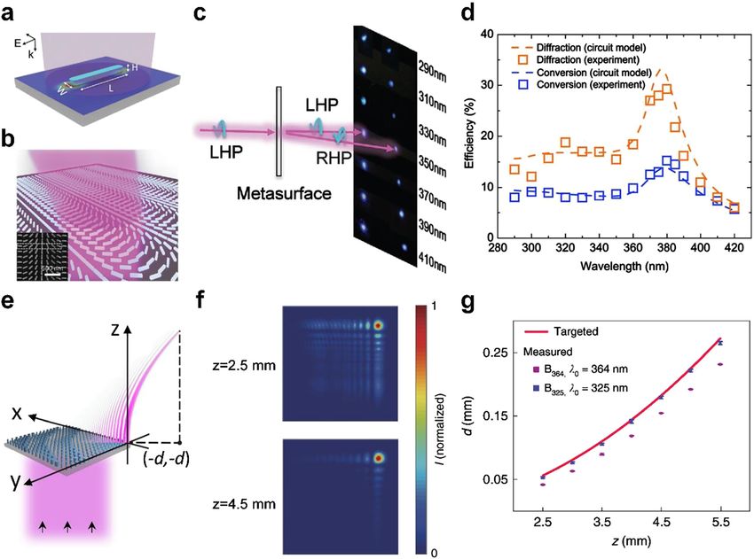
2288          D. Zhao et al.: Recent advances in ultraviolet nanophotonics

Figure 3: (a) Dispersion diagram for a plasmon mode in an MDM waveguide composed of Ag–Si3N4–Ag. Lezec et al. [51]. © 2007 The American
Association for the Advancement of Science. (b) Schematic drawing of negative refraction using Au-prism in an MDM waveguide.
(c) FDTD-calculated magnetic field distribution of the plasmon mode in an MDM waveguide when excited at normal incidence from free-space
at λ0 = 514 nm.

metamaterial behave as a volumetric bulk media with an                the wavevectors of light propagating inside the HMM. This
associated quasi-isotropic index (similar to other isotropic          has led to the use of HMMs in a variety of applications
media such as glass or air). In addition to performing                from creating ultrasmall cavities [57], promoting sponta-
negative refraction experiments to determine the refractive           neous emission [58, 59] or stimulated emission [60], en-
index (Figure 4d), researchers further utilized this planar           gineering thermal emission [61, 62], achieving enhanced
multilayer platform to demonstrate a Veselago flat-lens                absorption [63], realizing subdiffraction imaging [64, 65]
operating in the UV for the first time (Figure 4e). These              and facilitating asymmetric transmission [66].
experimental realizations of negative refraction and flat-
lensing using planar multilayer stack of alternating thin
films of metal and dielectric represents a paradigm shift in
how large-area planar metamaterials can be conceived
                                                                      4 Ultraviolet metasurfaces
without relying on complex lithographic patterning
                                                                      As two-dimensional embodiments of metamaterials, optical
requirements.
                                                                      metasurfaces are planar nanophotonic devices composed of
     Remarkably, dispersion engineering with such multi-
                                                                      spatially varying subwavelength nanostructures that could
layer approach is not just limited to achieving quasi-isotropic
                                                                      be designed to control the phase, amplitude, wavelength,
negative index of refraction. Instead, simple tweaking of the
                                                                      and polarization of light solely via engineering the geometry
layer thicknesses can result in the media acting as a hyper-
                                                                      and placement of the nanostructures [67–69]. The planar-
bolic metamaterial (HMM) [54–56]. An HMM is a uniaxial
                                                                      footprint and subwavelength thickness of metasurfaces
effective medium described by an isotropic relative magnetic
                                                                      enable their fabrication by using one-step top-down lithog-
permeability μ = 1 and diagonal relative electric permittivity
                                                                      raphy technologies used in mature semiconductor industries,
tensor that obeys ϵ′⊥ ϵ′∥ < 0, where ϵ⊥ = ϵ′⊥ + iϵ″⊥ and ϵ∥ =
                                                                      which avoids the challenging manufacturing requirements
ϵ′∥ + iϵ″∥ are respective complex effective relative permittiv-       for resonator based three-dimensional metamaterials and
ities for electric field components perpendicular and                  therefore pushing metadevices toward practical applications
parallel to the anisotropy axis of the HMM. Depending on              such as optics [70], quantum physics [71–73] and biology [74].
which of the two permittivity components, ϵ′⊥ or ϵ′∥ , is             The highly customizable nature of a metasurface allows it to
negative results in a type I (ϵ′∥ < 0) or type II (ϵ′⊥ < 0) HMM,      accomplish a variety of functions that have traditionally been
either of which can quite elegantly control and/or filter              fulfilled by a combination of bulk optical elements, such as
D. Zhao et al.: Recent advances in ultraviolet nanophotonics             2289

Figure 4: (a) Schematic drawing of all-angle negative refraction for a stack of three MDMDM unit-cells for excitation along the plane of the
layers (upper panel), and orthogonal to them (lower panel). TM polarized light is utilized in both cases. Verhagen et al. [52]. © 2010 American
Physical Society. (b) Left: schematic drawing of negative refraction from air into a metamaterial formed by three vertically stacked unit cells,
each consisting of planar layers of Ag–TiO2–Ag–TiO2–Ag. The structure is coated with a beam-defining mask consisting of a rectangular
aperture (width: 600 nm, length: 10 µm) in an opaque Cr film (thickness: 120 nm). Right: scanning electron microscopy image of cross-section
of a fabricated device. (c) FDTD-calculated magnetic field distribution of the plasmon mode in an MDMDM waveguide when excited at normal
incidence from free-space at λ0 = 364 nm. (d) Experimental values of refractive index (solid curve), and numerical values of refractive index
(dotted curve), as a function of angel of incidence θi , for TM-polarized light. Inset: FDTD-simulated magnetic field distribution for θi = 40°. Xu
et al. [53]. © 2013 Springer Nature. (e) Schematic drawing of a flat lens illuminated with UV light (purple). A sample object of ring shape placed
on one side of the flat lens is projected as a three-dimensional image in free space on the other side of the lens.

gratings, lenses, polarizers, wave plates, beam splitters, and             4.1 Working principles of ultraviolet
holograms, with a significantly reduced physical size                           metasurfaces
compared to traditional optical elements. Thus far, re-
searchers have demonstrated various types of high-                         Optical metasurfaces are typically designed according to
performance metasurfaces performing an array of function-                  several different principles, which can be categorized into:
alities such as beam steering [67, 75], high-resolution imaging            (1) propagation phase [95]; (2) geometric phase [87, 96, 97];
and display [76–83], hologram projection [84–87], structured               or (3) electromagnetic resonances [67, 98]. The principles
light generation [88, 89], asymmetric light transmission                   and applications of metasurfaces operating at visible up to
[90–92], and temporal pulse shaping [93, 94].                              microwave wavelengths have been discussed in several
2290         D. Zhao et al.: Recent advances in ultraviolet nanophotonics

previous works [99–104]. Due to high photon energy and               of polarization of the incident light. Such polarization-
strong material absorption of UV light [105], it is relatively       insenstive operation facilitates manipulation of light with
challenging to achieve high efficiencies for metasurfaces             various states of polarization, as well as unpolarized light.
operating in the UV region. With the advance of nano-                To realize high performance, the center-to-center spacing
fabrication techniques and employment of large-bandgap               between two neighboring nanopillars cannot be too small
materials, recent years have witnessed an exciting devel-            to minimize coupling between waveguide modes [114]. A
opment of compact metasurface-based UV optical ele-                  rule-of-thumb is to choose the nanopillar peridicity to be
ments as well as their diverse applications in holography            approximately one half of the targeted operational wave-
[106], lithography [107], photoemission spectroscopy [108]           length [115].
and information security [109]. In the following section, we
give a brief review of working principles used in the
                                                                     4.1.2 Geometric-phase ultraviolet metasurfaces
reported UV metasurfaces.

                                                                     Geometric-phase-based metasurfaces are composed of
4.1.1 Waveguide-based ultraviolet metasurfaces
                                                                     anisotropic nanostructures (Figure 5c) that exhibit
                                                                     different responses to two orthogonal electric-field
Waveguide-based metasurfaces usually rely on low-
                                                                     components (i.e., Ex and Ey) of the circularly polarized
absorption dielectric nanostructures of high refractive in-
                                                                     (CP) incident light [87, 111, 117, 118]. By rotating the
dex, which enables the formation of well-defined cavities
                                                                     nanostructures along a transverse plane, the cross-
with low-index background (Figure 5a). Light passing
                                                                     polarization part of the transmitted or reflected light will
through the dielectric nanostructure propagates in a
                                                                     immediately harvest a dispersion-free phase that equals
confined waveguide mode with its propagation properties
                                                                     twice of the rotation angle. Since this phase is induced
dependent on the shape and size of the nanostructure.
                                                                     by the geometry operation of the in-plane rotation and
When the lateral size of the planar nanostructure is modi-
                                                                     operates on both components of the cross-polarized
fied, the corresponding waveguide mode exhibits a
                                                                     light simultaneously, it is usually called as geometric
different mode volume, mode number, and field profile
                                                                     phase or Pancharatnam–Berry phase in memory of their
(Figure 5b), all of which could affect the amplitude and
                                                                     pioneer work [119]. To unveil the underlying physics in
phase of the transmitted light. With the aid of numerical
                                                                     geometric phase based metasurfaces, we assume that
modelling techniques such as finite-difference-time-
                                                                     light passing through individual nanostructures have
domain (FDTD) method and finite-element method (FEM),
                                                                     transmission coefficients of tx and ty for the Ex and E y
one can obtain the expected amplitude and phase modu-
                                                                     components, respectively. The electric field of CP light
lation imprinted on the transmitted light for a given wave-
                                                                     has the form of Eσ = E 0·[1, σi] T, where σ denotes the
guide geometry. Since such kind of metasurfaces modulates
                                                                     spin of circular polarization, and T represents the trans-
light via the presence of waveguide modes, we define them
                                                                     pose of a matrix. When a nanostructure is rotated by an
as waveguide-based metasurfaces. To realize high
                                                                     angle of θ, the vector electric field of transmitted light can be
operational efficiency in the UV, waveguide-based meta-
                                                                     expressed as
surfaces typically employ large bandgap materials, of
                                                                                                     ⎡        ⎤    ⎡ ⎤
which hafnium oxide (HfO2) is a representative one. With a                                             tx 0          1
                                                                                  Eout = E 0 ⋅ R(−θ)⎣         ⎦R(θ)⎣ ⎦
bandgap of ≈5.7 eV, HfO2 enables a transparency spectral                                               0 ty          σi            (1)
window down to free-space wavelength λ0 = 217 nm [106,                                    tx + ty      t x − ty 2iσθ
110]. To achieve both a high optical transmittance and wide                           =           Eσ +         e E−σ ,
                                                                                             2             2
range of phase modulation, waveguide-based metasurfaces
usually consist of high-aspect-ratio nanopillars [77, 111–                                                     cosθ      sinθ
                                                                     where the rotation operator R(θ) = [                     ]. In eq.
113]. As an example, the constituent nanopillars in previ-                                                     −sinθ     cosθ
ously-reported HfO2-based waveguide metasurfaces have                (1), one can find that the cross-polarization part in the
aspect ratios ranging from 3 to 10 [106]. In many cases,             transmitted light has an additional phase modulation of
nanopillars of circular in-plane cross-sections are employed         2σθ, which is independent of the operating wavelength. It
for waveguide-based metasurfaces, so that different phase            indicates that the geometric phase is the result of the
modulation can be implemeted by simply varying the                   interaction between the spin of photons and the geometric
diameter of the pillar. Moreover, thanks to the circular             coordinate of the objective physical system. The interac-
symmetry of its employed pillar, the metasurface's elec-             tion strength is determined by optical anisotropy of the
tromagnetic responses exhibit no dependence on the state             nanostructures, i.e., tx and ty.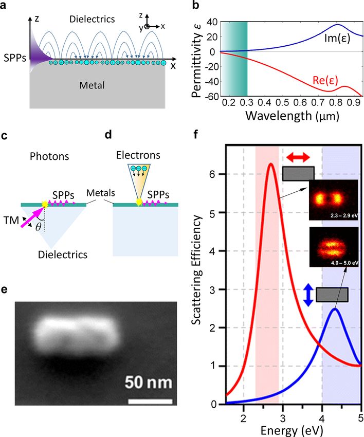
D. Zhao et al.: Recent advances in ultraviolet nanophotonics 2291
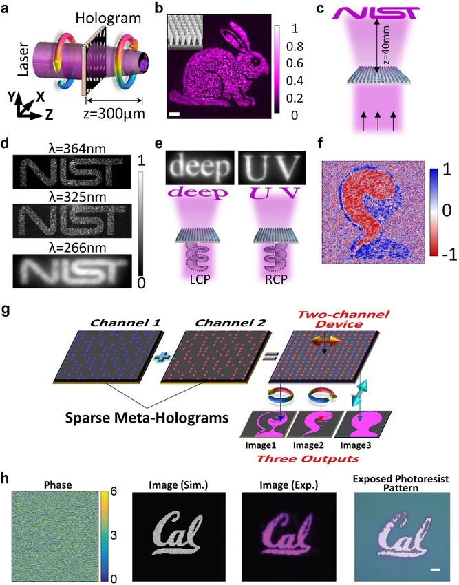
Figure 5: (a and b) SEM image (a) of HfO2-based waveguide metasurfaces and the electromagnetic nanomodes (b) resonating in the
nanopillars with different diameters ranging from d = 50 to 150 nm. Zhang et al. [106]. Author copyright. (c and d) SEM image (c) of Nb2O5-based
geometric metasurfaces and the antiferromagnetic resonances (d) in the nanostructures under the illumination of y-polarized light. Huang
et al. [109]. © 2019, WILEY‐VCH Verlag GmbH & Co. KGaA, Weinheim. (e and f) SEM image (e) of the ZnO-based resonance metasurfaces and the
simulated magnetic dipoles (f) confined in the nanostructure. Semmlinger et al. [116]. © 2018 American Chemical Society.
If tx = −ty = 1 in eq. (1), the anisotropy is maximized Therefore, such antiferromagnetic resonances hold the
such that the nanostructures work as high-efficiency fundamental mechanism of nanoscale half waveplates
nanoscale half waveplates due to the phase delay of π in dielectric geometric metasurfaces. At UV wavelengths,
between two orthogonal electric-field components of light. high-efficiency dielectric geometric-phase-based meta-
To enhance the optical transmission of nanostructures, it surfaces require low-loss materials such as Nb2O5 [109] or
requires coexistence of both electric and magnetic reso- HfO2 [106], which have their transparency windows located
nances [120], such that the electric and magnetic dipoles at wavelengths λ > 340 nm and λ > 217 nm, respectively. At
have vertical orientation [98]. In dielectric nanostructures, even-smaller wavelengths (vacuum UV and soft X-ray
the magnetic dipoles can be induced by a circulating light), all dielectric materials are absorbing [105] hence
electric displacement current [121]. It has been found that such antiferromagnetic-resonance-based geometric meta-
antiferromagnetic modes containing several antiparallel surfaces will not work.
magnetic dipoles (AMDs) usually appear in nanoscale In contrast, the optical anisotropy of a nanostructure is
dielectric half waveplates [109]. More importantly, the minimum for tx = ty that appears in symmetric, circular-,
AMDs induced by the Ex and Ey components have odd and and square-shaped, nanostructures. In the transmitted
even values, respectively. The electric-field vectors of light light, the cross-polarization component is zero but the
at the input and output ends of the nanostructure are copolarization part has no geometric phase modulation. It
reversed for odd AMDs (Figure 4d) but stays the same for means that circular and square nanostructures cannot be
even AMDs. It implies that the phase delay is π for Ex but used for geometric-phase-based metasurfaces. However, if
0 for Ey, thus realizing the functionality of a half waveplate. tx ≠ ty in eq. (1), the cross-polarization part survives, leading
2292         D. Zhao et al.: Recent advances in ultraviolet nanophotonics

to the possibility of demonstrating geometric-phase-based            Similarly, toroidal modes considered as nonradiating
metasurfaces across the entire electromagnetic spectrum.             monopoles can be excited by metallic meta-atoms
For example, although Si is highly absorbing at UV wave-             composed of two mirror-symmetry ‘D’-like nanostructures
lengths, a 32 nm wide and 142 nm long Si nanorod was                 [43]. Although these two approaches has been demon-
demonstrated to work as a UV geometric-phase metasur-                strated at UV wavelengths, other methods, such as single
face element from λ = 280 nm to λ = 400 nm [107], due to the         electric dipole resonance [124], or simultaneous excitation of
unequal transmission for Ex and Ey components of light.              electric and magnetic resonances [98] can also be used for
Even using subwavelength rectangular air-holes etched in             UV metasurfaces. From the viewpoint of wavefront shaping,
a metal film [122], an UV geometric-phase metasurface has             a transmissive metasurface based on only single electric or
been demonstrated without plasmonic resonances at a                  magnetic dipole can only have a maximum phase modula-
wavelength of 355 nm. These results suggest that nonres-             tion of π and their efficiency is limited to  3.3 eV) are preferred as the constituent materials for
magnetic dipole by using circle electric displacement cur-           metasurface fabrication. Representative wide-bandgap
rents at the 395 nm wavelength [116], as shown in Figure 5f.         dielectric materials include Silicon Dioxide (SiO2,
D. Zhao et al.: Recent advances in ultraviolet nanophotonics    2293

Eg ≈ 9.0 eV), Niobium Pentoxide (Nb2O5, Eg ≈ 3.65 eV),          patterns are completely filled, and at the same time, a
Hafnium Oxide (HfO2, Eg ≈ 5.7 eV), Aluminum Nitride             quasi-planar dielectric layer is formed on top of the resist
(AlN, Eg ≈ 6.0 eV), and Silicon Nitride (Si3N4, Eg ≈ 5.0 eV).   layer. Following ALD, the overcoated dielectric layer is
The materials’ refractive indices in the UV region are          back-etched to the resist top surface. Finally, the
plotted in Figure 6a and b. Among them, SiO2 exhibits the       remaining resist is removed, yielding high-aspect-ratio,
lowest refractive index and is readily obtained in the          straight dielectric nanostructures of uniform height and
form of high-quality, large-scale wafers. Therefore, SiO2       smooth side-wall profiles (Figure 6c and d). Utilizing such
(usually in the form of fused-silica) is typically employed     Damascene process, researchers have successfully
as the substrate material for UV metasurface devices. In        implemented Nb2O5-based devices operating in the
purely numerical studies, AlN and Si3N4 have been               near-UV region and performing hologram projection
employed to design metalenses operating down to the             [109], as well as HfO2-based devices operating in the near-
deep-UV. In experimental works, Nb2O5 has been used to          and deep-UV regions and performing high-numerical-
construct high-performance devices operating at near-UV         aperture lensing, hologram projection, and Airy beam
wavelengths (λ0 = 355 nm) [109]. Moreover, HfO2, with           generation [106].
an even wider bandgap, has been employed to realize
efficient metasurface devices operating down to the
record-short deep-UV region [106]. Diamond has also             5 Applications
been suggested in theory to shape UV light but without
any experimental demonstration because of lack of access        As mentioned above, plasmonic effect as the collective
to large-scale thin diamond film and the associated              oscillations of electrons is one intrinsic property of material
fabrication challenges, although diamond has a large            and can be excited with the help of nanostructures. In
bandgap of ≈5.5 eV and high refractive index of ≈2.4 [127].     comparison, metamaterials and metasurfaces are artificial
Here, we summarize the materials used in UV nano-               nanostructures that exhibit engineered optical properties
photonics, as shown in Figure 6e. The small-bandgap             of materials. Therefore, the plasmonic materials have been
materials such as GaN [78], TiO2 [80] and Nb2O5 [109]           frequently utilized in metamaterials and metasurfaces for
usually work in near-UV region. Si3N4 [51], diamond [127],      various optical devices, where the plasmonic resonances
AlN [128], HfO2 [106] work in the deep-UV region due to         could compensate electromagnetic responses required
their bandgaps larger than 4.43 eV. In addition, their          in metamaterials and metasurfaces. For simplicity of
refractive index is larger than 2, which is sufficient to        discussion, we only introduce UV devices assisted by the
demonstrate the metasurfaces. In comparison, CaF2 [129],        field-enhancement effect of plasmons as well as plasmonic
SiO2 [130], and MgF2 [131] with even larger bandgaps have       based UV optical elements in Section 5.1, leaving UV
low refractive indices so that they usually are employed as     plasmonic metamaterials and metasurfaces in Section 5.2.
the substrate in UV metasurfaces.                               In addition, considering that metamaterials are difficult to
     One difficulty of implementing wide-bandgap                fabricate in practical applications, we summarize all
dielectric-based UV metasurfaces is fabrication of              applications related to UV metamaterials and metasurfaces
subwavelength-scale, high-aspect-ratio nanostructures.          in Section 5.2, where metalenses, beam steering, hologra-
Though directional reactive etching has been demon-             phy, photoemission spectroscopy, and nonlinear optics are
strated as a straightforward and effective method to            addressed with detailed discussions and summary of
pattern dielectric materials such as Si [93, 95] or GaN [78],   important advances.
the corresponding etching recipes for patterning many of
the aforementioned wide-bandgap materials are instead
rather underexploited or even impractical. To overcome          5.1 Plasmonics-assisted ultraviolet devices
such limitations, a resist-based Damascene process has
been developed. During this process, metasurface pat-           Highly confined nature of SPPs result in a strong field
terns are first created in the resist layer by lithography.      enhancement at the interface with air in metal films or at
Then, low-temperature atomic layer deposition (ALD) is          the corners or edges of metallic nanostructures. This field
utilized to conformally fill in the holes and trenches of the    enhancement is extremely helpful for various optical
developed resist layer with the targeted wide-bandgap           effects that depend on the electric field in a nonlinear
dielectric material. ALD is intentionally performed over a      manner, e.g., facilitating the observation of photon-created
long duration such that all openings of the exposed resist      carriers in photodetectors, and increasing the optical field
2294 D. Zhao et al.: Recent advances in ultraviolet nanophotonics
Figure 6: (a and b) Refractive index n (a) and
extinction coefficient k (b) of representative
UV-transparent dielectric materials. The
legend in (b) applies to (a). (c) Scanning
electron microscopy image of a HfO2-based
metasurface operating in the deep-UV.
Zhang et al. [106]. Author copyright. (d)
Scanning electron microscopy image of a
Nb2O5-based metasurface operating in the
near-UV. Huang et al. [109]. © 2019, WILEY‐
VCH Verlag GmbH & Co. KGaA, Weinheim.
(e) Common optical materials used in UV
nanophotonics.
in Raman processes. Here, we introduce the roles of In addition to temperature dependence, low dark current
plasmonics in UV photodetectors and Raman needs large work function of materials to decrease the
spectroscopy. escaping possibility of the thermally excited electrons.
However, the large work function also reduces the escape
5.1.1 Plasmonic ultraviolet photodetectors possibility of the photogenerated carriers, thereby leading
to low responsivity. Technically, cooling is the most
Photodetectors are important optoelectronic devices that efficient method to suppress dark current and is typically
transduce incident photons into excited electrons and used in various photodetectors.
holes, to create an electric current [132]. The escaped In comparison, it is desirable to realize high respon-
electrons from the surface of materials must overcome its sivity UV photodetectors, which will be quite useful for
work function, which is relative to the surface potential. weak-light or single-photon detection for applications in
Most UV photodetectors adopt a large-bandgap material chemistry, quantum optics, and astronomy. In addition to
such as GaN as the host material due to its good chemical the avalanche-type mechanism, high-responsivity UV
and thermal stability enabling a longer lifetime of the photodetectors also employ localized SPPs that provide
created hot carriers [132]. Low dark current and high strong field enhancement [44], which helps to decrease the
responsivity are the key properties for photodetectors, but surface potential of materials around the plasmonic
it is difficult to achieve both of them simultaneously [133]. nanoparticles [134]. It decreases the work function andD. Zhao et al.: Recent advances in ultraviolet nanophotonics 2295
increases the escape possibility of photogenerated elec- of molecules or atoms is an intrinsic property determined
trons, therefore enhancing the responsivity. An UV by the chemical bonding for a given material and can be
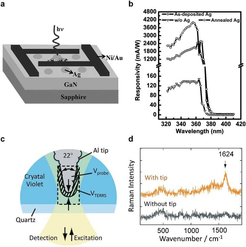
photodetector with gold nanoparticles patterned on the seldom modified by incident photons. In comparison,
surface of GaN (Figure 7a) exhibit ≈30 times enhancement enhancement of the incident intensity is usually achieved
in the responsivity than the bare GaN-based detector at the by using the plasmonic resonances at rough surface of
UV spectrum ranging from λ = 320 nm to λ = 380 nm metals, which is the underlying physical origin of surface-
(Figure 7b) [44]. Another AlGaN-based UV photodetector enhancement Raman scattering (SERS). For a plasmonic
with plasmonic effects induced by aluminum nano- surface, the Raman scattering intensity is proportional to
particles has been reported with a twofold enhancement in the fourth power of the electric-field enhancement factor.
the responsivity at wavelengths below 300 nm [135]. More Although many SERS spectroscopies have been demon-
UV photodetectors on the basis of other mechanisms such strated with the silver and gold at the visible and infrared
as avalanche effects and p–n heterojunctions have already wavelengths, they are not efficient in characterizing the
been well reviewed in other works [132, 133, 136]. organic and inorganic molecules with small scattering
cross section. Meanwhile, the Raman and fluorescence
5.1.2 Plasmonic ultraviolet surface-enhancement spectra at the visible and infrared can overlay on top of
Raman scattering each other, increasing the background noise of Raman
signal. Fortunately, SERS signal under UV-light excitation
Raman scattering is an inelastic light–matter interaction can solve these issues due to its high photon energy.
that enables some of the scattered photons to carry slightly The first UV SERS was demonstrated with a Raman
different frequencies determined by optical phonons enhancement of >2 orders of magnitude on rhodium and
corresponding to the polarizability of molecules or atoms ruthenium electrodes under the 325 nm wavelength exci-
inside solids or some liquids [137]. The scattering intensity tation [42]. At the same wavelength, another enhanced
at the Raman frequency depends on the polarizability SERS was also reported by using Au electrodes [138].
enhancement and the incident intensity. The polarizability Although these two pioneering works reported exciting
Figure 7: (a and b) A GaN-based UV photo-
detector with plasmonic enhancement via
Ag nanoparticles (a) and its measured
responsivity at the UV wavelengths (b). Li
et al. [44]. © 2012 WILEY‐VCH Verlag GmbH
& Co. KGaA, Weinheim. (c and d) Tip-
enhanced Raman scattering spectroscopy
(c) and a comparison of the experimental
Raman intensity between the cases with
and without tip (d). © 2009 John Wiley &
Sons, Ltd.2296 D. Zhao et al.: Recent advances in ultraviolet nanophotonics
SERS enhancement results, the role of SPPs during the HfO2 has been employed to construct high numerical
process was not revealed or discussed comprehensively. aperture (NA = 0.6) metalenses operating at near-UV
Meanwhile, the employed metals such as rhodium, ruthe- wavelengths of 364 and 325 nm (Figure 8a). The nanoscale
nium, and gold cannot support deep-UV plasmon reso- building blocks of the UV metalenses consist of high-
nances. A better approach by using a thin Al layer for the aspect-ratio HfO2 circular nanopillars of varying radii
UV SERS was reported in 2007 by Popp’s group for an arrayed on a fused silica substrate with subwavelength
excitation wavelength of 245 nm [139], which opens more spacing. Each element acts as a truncated dielectric
opportunities for UV SERS. For example, an Al-coated waveguide, through which light propagates with trans-
nanotip under the 266 nm deep-UV excitation exhibits a mission intensity and phase shift controlled by the
Raman enhancement of ≈60 to 200 times for various cylinder height, cylinder radius, and lattice spacing. For
samples such as crystal violet solution and films [140], as the targeted operation wavelength of 364 nm (325 nm), a
shown in Figure 7c and d. In addition, benefitting from cylinder height of 550 nm (500 nm), lattice spacing of
resonant Raman effects, caused by the fact that the 200 nm (190 nm), and radius variation range of 50–160 nm
bandgaps of some DNA and proteins are located at the UV (50 –150 nm) are chosen. For both devices, the measured
spectrum, the Raman signal of adenine molecules had an intensity distribution reveals lensing with a circularly
enhancement of ≈5 on the top of an Al nanoparticle array symmetric focal spot, of first-dark-ring diameter close to
[141], compared with the case on the fused silica. Mean- the theoretical diffraction-limited value (Figure 8b and c).
while, the achieved signal-to-noise ratio of ≈50 indicates The focusing efficiency, defined as the ratio of the optical
that the UV SERS spectroscopy holds the great promise for power in the focused spot to the total power illuminating
ultrasensitive detection and characterization of biological the metalens, are 55.17% (for the 364-nm metalens) and
issues and molecules. 56.28% (for the 364-nm metalens).
5.2.2 Metasurface-based beam steering
5.2 Ultraviolet metaoptics
Traditionally, changing the propagation direction of
Due to the challenge of material absorption and fabrication light can be realized by using optical reflection with a
constraints, the development of UV metasurfaces has only mechanically rotating mirror that is the key element of
begun since 2018 [43, 107, 116]. Driven by the requirements Galvo scanning systems in optical display projectors, mi-
for industrial applications, UV metasurfaces have har- croscopes, and LiDAR. Such a traditional mechanical
vested increasing attention due to its compact volume and approach is usually bulky, which is not preferred for
powerful wavefront shaping capabilities. Novel UV meta- portable or integrated systems. Although mirrors based on
devices have been demonstrated for various applications microelectromechanical systems (MEMS) could shrink the
such as lenses, beam steering, holography, photoemission length scale to several tens of micrometers, the tuning
spectroscopy and nonlinear phenomena. Here, we review angle for most commercial MEMS mirrors is limited to
the experimental advances of these UV metadevices. below ±20°, which are insufficient in many applications
such as large-area imaging or intelligent vehicles. The
5.2.1 Metalens alternative method for beam steering is to add an
additional tiling phase into the incident beam by using a
Conventional optical lenses control the wavefront of light pure-phase element, such as a spatial light modulator
through a continuous phase gradient that is accumulated (SLM) [145] or using metasurfaces. The tilting angle is
when light propagates through a transparent optical determined by the period of the phase element. The
medium having spatially varying thickness. This working smallest pixel pitch of SLMs is ≈3.74 μm (Holoeye Gaea),
principle yields bulky three-dimensional (3D) material pro- which allows the maximum tilting angle of only a few de-
files that are challenging to manufacture within the required grees at the UV and visible wavelengths. Due to the sub-
wavefront error tolerance, as well as to integrate into wavelength pixel pitch, metasurfaces are one of the
compact, miniaturized systems. In contrast, metasurface- promising candidates for large-angle steering. Figure 9a
based lenses (metalenses) take a radically different and b sketches Si-based geometric-phase-based meta-
approach to achieve the same functionality and output surfaces composed of nanorods with their orientation
phase profile, which is by using a planar array of phase- angle dependent on the location [107]. Within a period of
shifting elements of subwavelength dimensions and 160 nm, eight nanorods are used to realize a full-phase
spacing [142–144]. modulation of 2π, resulting in a tilting angle of ±13.1° atD. Zhao et al.: Recent advances in ultraviolet nanophotonics 2297
Figure 8: (a) Schematic drawing of focusing by a UV metalens, L364 or L325, under normal-incidence, plane-wave illumination at free-space
wavelength of λ0 = 364 or 325 nm, respectively. (b and c) Cross-focus cuts and intensity distributions in the focal plane, as measured for
metalenses L364 and L325, respectively. The theoretically predicted cross-focus cuts are plotted for reference. Scale bars: 1 µm. Zhang et al.
[106]. Author copyright.
λ = 290 nm and ±17.3° at λ = 380 nm (Figure 9c). Their Nb2O5 with a bandgap of ≈3.65 eV, an UV metahologram
experimentally demonstrated efficiency is ≈10% from operating at 355 nm wavelength has been reported with an
λ = 280 nm to λ = 420 nm (Figure 9d). The tilting angle can experimental efficiency of ≈79.6% [109], which is a
be further enlarged by decreasing the number of nanorods record-high efficiency for all UV metasurfaces and meta-
in a full phase cycle of 2π, which, however, decreases the devices demonstrated till date (Figure 10a and b). Another
efficiency of the tilting beam. Considering the strong geometric metahologram by using HfO2 nanorods extends
absorption of silicon at the UV spectrum, the upper limit on the operating spectrum down to λ = 325 nm and λ = 266 nm
efficiency is ≈10%. (Figure 10c and d) [106], meanwhile harvesting impres-
HfO2 with a bandgap of 5.7 eV is a low-loss material sively high efficiency(≈71.78% at λ = 325 nm and ≈60.67%
platform for the wavefront shaping of light. The waveguide at λ = 266 nm). Both works verify that the UV metasurfaces
metasurfaces made of circular HfO2 nanopillars have been have a great potential for practical applications because
reported to create an UV Airy beam with a cube phase profile they have solved the efficiency problem. Note that,
that could make the light beam propagate along a curved although both materials Nb2O5 and HfO2 have large
trajectory without any significant divergence [106], illus- bandgap, their refractive indices are ≈2, which is slightly
trating a nondiffraction feature (Figure 9e). The measured higher than SiO2 or quartz substrate. It leads to a
intensity profiles and the experimental trajectories at requirement of high-aspect-ratio nanostructures, e.g., 7
various wavelengths are shown in Figure 9f and g, respec- for Nb2O5 nanobricks [109] and 3–10 for HfO2 nanorods
tively. Benefiting from the large bandgap, their measured [106], which are challenging to fabricate via the dry
efficiency is ≈47% at λ = 364 nm and ≈67% at λ = 325 nm, etching process. Therefore, both works utilize the afore-
which are the highest efficiency at these selected wave- mentioned electron-beam lithography (EBL) combined
lengths and therefore makes UV metasurfaces comparable with ALD technique to fabricate the metasurfaces.
to visible and infrared metasurfaces. Ultraviolet geometric-phase-based metasurfaces could
also realize polarization-multiplexed holograms because
5.2.3 Metaholography the geometric phase is dependent on the handedness of
the input circular polarization. A spin-multiplexed meta-
As another demonstration of wavefront engineering, UV hologram operating at a wavelength of 266 nm is shown
metasurface holograms have drawn a great deal of to create two spin-dependent images. When a left-handed
attention due to their potential applications in informa- CP light illuminates the metahologram, an image of “deep”
tion security and lithography. All reported UV metaholo- is constructed at a distance z = 40 mm away from the
grams employ geometric phase that can be easily metasurface (Fresnel region of the metahologram with a
controlled by the orientation of a fixed-size nano- size of 330 μm × 330 μm), while the right-handed CP light
structure, which facilitates fabrication due to uniformity yields the different image of “UV” (Figure 10e) [106]. The
in nanostructures shape and size. By using semiconductor phase loaded on the hologram is the weighted super-2298 D. Zhao et al.: Recent advances in ultraviolet nanophotonics Figure 9: Beam steering by using UV metasurfaces. (a) Sketch for the working principle of Si-based UV geometric metasurfaces. (b) Image of UV metasurfaces for beam steering. (c) Experimental results for steering the UV at the different wavelengths. (d) Measured efficiency of this metasurfaces over a broadband spectrum. Deng et al. [107]. © 2018 WILEY‐VCH Verlag GmbH & Co. KGaA, Weinheim. (e and f) Sketch for steering the beam along a curved trajectory (e) via the Airy beam (f). (g) A comparison between the experimental and ideal trajectories at the different z cut planes. Zhang et al. [106]. Author copyright. position of both phase profiles for left- and right-handed CP approaches realize the holographic reconstruction at the light, and is used to determine the orientation angle of Fresnel region, where the image is real for one spin but nanostructures in the metahologram. In comparison, becomes virtual for the reversed spin [96, 146]. In contrast, another spin-multiplexed UV metaholograms employs two the Fraunhofer metaholograms have center-symmetric real interleaved apertures [109], each of which encodes two images for both spins [147]. A united mathematical expla- spin-dependent sparse holograms (Figure 10f). One sparse nation has been given in a newly published book [148]. metahologram for left-handedness CP light reconstructs an In addition to optical anticounterfeiting, UV meta- image of “girl” pattern at the Fresnel region, while the holograms has also been used for optical lithography other hologram for right-handedness CP light creates the because high energy of UV photons can help to break complementary “snake” pattern. Both “girl” and “snake” chemical bonds of molecules in some photoresists such as patterns are complementary to each other so that their polymethyl methacrylate (PMMA) and Hydrogen silses- combined pattern is observed as another image of “tro- quioxane (HSQ). An ultrathin (40 nm thickness) Si meta- phy”. Thus, one can directly see a picture of “trophy” under hologram operating at λ = 380 nm creates the image “Cal”, the linear-polarization illumination. After the polarization which is used to expose the photoresist [107]. The exper- analysis, the pattern “trophy” exhibits a vector feature imental results are shown in Figure 10h, which indicates (Figure 10g), which can provide an additional degree of good performance. Considering the interference speckles freedom for the purpose of optical anticounterfeiting. It is created in the holographic image, a dynamic random attributed to the spin multiplexing functionality of geo- phase provided by a rotating optical diffuser is used to metric metasurfaces. Note that, both spin-multiplexing increase the coherence of the diffracted light, thus
You can also read