Universal mechanical exfoliation of large-area 2D crystals - arXiv
←
→
Page content transcription
If your browser does not render page correctly, please read the page content below
Universal mechanical exfoliation of large-area 2D crystals
Yuan Huang1†, Yu-Hao Pan2†, Rong Yang1†, Li-Hong Bao1, Lei Meng1, Hai-Lan Luo1,
Yong-Qing Cai1, Guo-Dong Liu1, Wen-Juan Zhao1, Zhang Zhou1, Liang-Mei Wu1,
Zhi-Li Zhu1, Ming Huang3, Li-Wei Liu4, Lei Liu5, Peng Cheng1, Ke-Hui Wu1,
Shi-Bing Tian1, Chang-Zhi Gu1, You-Guo Shi1, Yan-Feng Guo6, Zhi Gang Cheng1,7,8,
Jiang-Ping Hu1,7,8, Lin Zhao1,7,8, Eli Sutter9, Peter Sutter10*, Ye-Liang Wang1,4, Wei
Ji2*, Xing-Jiang Zhou1,7,8*, and Hong-Jun Gao1,7*

1
    Institute of Physics, Chinese Academy of Sciences, Beijing 100190, China
Department of Physics and Beijing Key Laboratory of Optoelectronic Functional Materials
2

& Micro-Nano Devices, Renmin University of China, Beijing 100872, China
3
 School of Materials Science and Engineering, Ulsan National Institute of Science and
Technology (UNIST), Ulsan 44919, Republic of Korea
School of Information and Electronics, MIIT Key Laboratory for Low-Dimensional
4

Quantum Structure and Devices, Beijing Institute of Technology, Beijing, 100081, China
5
    College of Engineering, Peking University, Beijing 100871 China
School of Physical Science and Technology, Shanghai Tech University, Shanghai 201210,
6

China
7
    University of Chinese Academy of Sciences, Beijing, 100049, China
8
    Songshan Lake Materials Laboratory, Dongguan, 523808, China
9
 Department of Mechanical and Materials Engineering, University of Nebraska—Lincoln,
Lincoln, Nebraska 68588, United States
 Department of Electrical and Computer Engineering, University of Nebraska—Lincoln,
10

Lincoln, Nebraska 68588, United States

†These authors contributed equally to this work.
*Correspondence to: psutter@unl.edu (P.S.); wji@ruc.edu.cn (W.J.); xjzhou@iphy.ac.cn
(X.J.Z.); hjgao@iphy.ac.cn (H.J.G.)

                                                1
Abstract
Two-dimensional (2D) materials provide extraordinary opportunities for exploring
phenomena arising in atomically thin crystals1-4. Beginning with the first isolation of
graphene5, mechanical exfoliation has been a key to provide high-quality 2D materials
but despite improvements it is still limited in yield6, lateral size and contamination.
Here we introduce a contamination-free, one-step and universal Au-assisted
mechanical exfoliation method and demonstrate its effectiveness by isolating 40 types
of    single-crystalline   monolayers,        including   elemental    2D     crystals,
metal-dichalcogenides, magnets and superconductors. Most of them are of
millimeter-size and high-quality, as shown by transfer-free measurements of electron
microscopy, photo spectroscopies and electrical transport. Large suspended 2D
crystals and heterojunctions were also prepared with high-yield. Enhanced adhesion
between the crystals and the substrates enables such efficient exfoliation, for which
we identify a common rule that underpins a universal route for producing large-area
monolayers and thus supports studies of fundamental properties and potential
application of 2D materials.

                                          2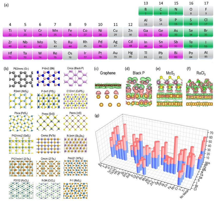
Main
     Two-dimensional (2D) materials continue to reveal dimensionality-correlated
quantum phenomena, such as 2D superconductivity, magnetism, topologically
protected states, and quantum transport1, 7-11. Stacking 2D materials into van der Waals
heterostructures leads to further emergent phenomena and derived device concepts12,
 . The further discovery and application of new properties depend on the
13

development of synthesis strategies for 2D materials and heterostructures6,         14-18
                                                                                            .
Synthesis using crystal growth methods can now produce large (millimeter-scale)
single crystals of some 2D materials, notably graphene and hexagonal boron nitride,
but the scalable growth of high-quality crystals has remained challenging18, 19, with
many 2D materials and especially heterostructures proving difficult to realize by
bottom-up approaches. Ion-intercalation and liquid exfoliation are used as top-down
approaches but, as chemical methods, they often cause contamination of the isolated
2D surfaces20, 21. While some gold-assisted exfoliation methods were demonstrated in
layered chalcogenides22-24, those methods still bring unexpected contamination in
samples prepared for electrical and optical measurements and thus reduce their
performances when removing gold films with chemical solvents in additional steps. In
light of this, a contamination-free, one-step and universal preparation strategy for
large-area, high-quality monolayer materials is still lacking for both fundamental
research and applications.
     In the past 15 years, mechanical exfoliation has been a unique enabler of the
exploration of new 2D materials. Most intrinsic properties of graphene, such as the
quantum Hall effect25, massless Dirac Fermions26, and superconductivity27, were
mostly observed on exfoliated flakes but are either inaccessible or suppressed in
samples prepared by other methods17,     28
                                           . While exfoliation often suffers from low
yield and small sizes of the exfoliated 2D flakes5, many layered materials are,
however, yet to be exfoliated into monolayers by established exfoliation methods.
Such challenge of exfoliation limits their utility for scalable production of 2D crystals
and complicates further processing, e.g., to fabricate heterostructures. These issues
could be resolved by identifying suitable substrates that firmly adhere to 2D crystals
                                              3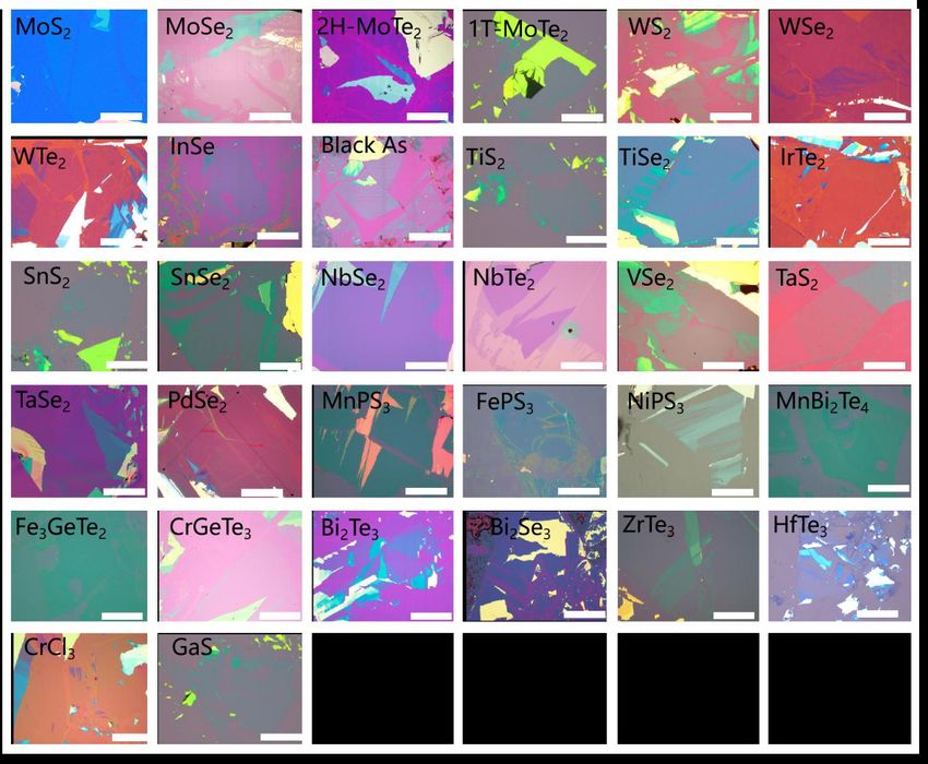
without compromising their structure and properties, thus allowing the separation and
transfer of the entire top sheet from a layered bulk crystal. Covalent-like
quasi-bonding (CLQB), a recently uncovered non-covalent interaction with typical
interaction energies of ~0.5 eV/unit cell29-31, fits the requirements of the craving
interaction between substrates and 2D layers. The intermediate interaction energy for
CLQB is a balance of a reasonably large Pauli repulsion induced by interlayer
wavefunction overlap and an enhanced dispersion attraction caused by more
pronounced electron correlation in 2D layers with high polarizability.
   Promising candidate substrates for CLQB with 2D crystals are materials whose
Fermi level falls in a partially filled band with mostly s- or p-electrons to prevent
disrupting the electronic structure of 2D layers, and which have highly polarizable
electron densities to ensure a large dispersion attraction. Noble metals meet these
criteria and are easily obtained as clean solid surfaces. Group 11 (IB) coinage metals,
i.e., Cu, Ag and Au, remain as potential candidates after ruling out Pt of high melting
temperature, other group 8-10 (VIII) metals of too strong hybridization, Al of high
activity to 2D layers and in air32, 33 and closed-shell group 12 (IIB) metals (Zn, Cd,
Hg). Among those three, Au interacts strongly with group 16 (VIA) chalcogens (S, Se,
Te) and 17 (VIIA) halogens (Cl, Br, I), which terminate surfaces in most 2D materials.
Together with its low chemical reactivity and air stability, Au appears promising for
high-yield exfoliation of many 2D materials, which is also evidenced by three
previous attempts22-24.
   Density functional theory (DFT) calculations were employed to substantiate these
arguments by comparing the interlayer binding energies of a large set of layered
crystals with their adhesion energies to the Au (111) surface. A total of 58 layered
materials, including 4 non-metallic elemental layers and 54 compounds comprised of
metal and non-metal elements were considered in our calculations (see Fig. 1a). They
belong to 18 space groups covering square, hexagonal, rectangular and other lattices
(Fig. 1b). The surfaces of all considered compound layers are usually terminated with
group 16 (VIA) or 17 (VIIA) elements, e.g., S, Se, Te, Cl, Br and I, with the exception
of W2N3. These atoms, together with group 15 (VA) elements, are expected to have
                                           4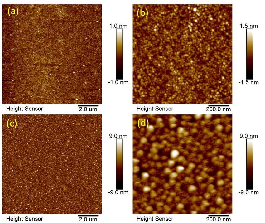
substantial interactions with Au substrates, which is verified by our differential charge
density (DCD) plots.

Fig. 1. DFT calculated interlayer binding energies of 2D materials and adsorption energies on Au
(111) surfaces. (a) Part of the periodic table, showing the elements involved in most 2D materials
between groups 4 (IVB) and 17 (VIIA). (b) Eighteen space groups and typical structural configurations
(top views) of the 2D materials. (c-f) DCD of four Au (111)/2D crystal interfaces with (non-metallic)
terminating atoms between groups 14 (IVA) and 17 (VIIA). Isosurface values of these DCD plots are
5×10⁻⁴ e/Bohr3 (graphene), 1×10⁻² e/Bohr3 (BP), and 1×10⁻³ e/Bohr3 (MoS2, RuCl3), respectively. (g)
Bar graph comparing the interlayer binding energies of 2D materials (blue cylinders) with their
adsorption energies on Au (111) (red cylinders). The visible red cylinders represent the difference
between the Au/2D crystal interaction and the interlayer interaction.

    Figs. 1c-f show the DCDs of graphene, black phosphorus (BP), MoS2, and RuCl3
monolayers adsorbed on Au (111), representing the interactions of Au with group 14
(IVA) to 17 (VIIA) atoms, respectively. The adhesion induced charge redistribution of
graphene differs from those of the other three layers. While Au only introduces charge
dipoles at the interface to graphene, significant covalent characteristics, i.e., charge
reduction near the interfacial atoms and charge accumulation between them, were
                                                    5
observable at the P/Au, S/Au and Cl/Au interfaces. The difference in charge
redistribution is reflected in the smaller adhesion energy of graphene/Au (28 meV/Å2;
0.15 eV/unit cell) compared with those of the other three interfaces (56, 40 and 36
meV/Å2; 0.80, 0.35 and 1.11 eV/unit cell). The clearly covalent nature of the S/Au
interface is consistent with previous reports22-24 and confirms our expectation. Our
results of DCD and electronic band structures (Fig. S1), suggest the existence of
CLQB at the S/Au, P/Au and Cl/Au interfaces, which is confirmed by comparing the
interlayer (0.23, 0.48 and 0.57 eV/unit cell) and 2D crystal/Au (0.35, 0.80 and 1.11
eV/unit cell) binding energies. Fig. 1g and Table S1 show the comparison of these
energies for all 57 considered 2D crystals, where the 2D crystal/Au binding is
invariably stronger than the corresponding interlayer binding. These results support
the concept that the 2D crystal/Au interaction should be sufficient to overcome the
interlayer attraction and facilitate exfoliating monolayers from a broad range of
layered crystals. Here, we define a ratio RLA/IL as layer-Au over interlayer adhesion
energies. Possible exceptions are those 2D materials whose RLA/IL values, while
greater than 1, are substantially smaller than usual RLA/IL values (>1.3). Here, BN
(1.07), GeS2 (1.17) and graphene (1.24) are some examples.
    To test these theoretical predictions, we implemented the Au-assisted exfoliation
of 2D materials as shown in Fig. 2a. Firstly, a thin layer of Au is deposited onto a
substrate covered with a thin Ti or Cr adhesion layer. Then, a freshly cleaved layered
crystal is brought in contact with the Au layer. Adhesive tape is placed on the outward
side of the crystal, and gentle pressure is applied to establish a good layered
crystal/Au contact. Peeling off the tape removes the major portion of the crystal,
leaving one or few large-area monolayer flakes on the Au surface. Limited only by the
size of available bulk crystals, these monolayer flakes are usually macroscopic in size
(millimeters; see Methods for details).
     Optical microscopy was used to examine the dimensions and uniformity of the
exfoliated 2D crystals. Fig. 2b shows an image of exfoliated MoS2 monolayers
reaching lateral dimensions close to 1 cm on a SiO2/Si substrate covered with Au (2
nm)/Ti (2 nm). We also extended the base substrate from the SiO2/Si substrate to
                                          6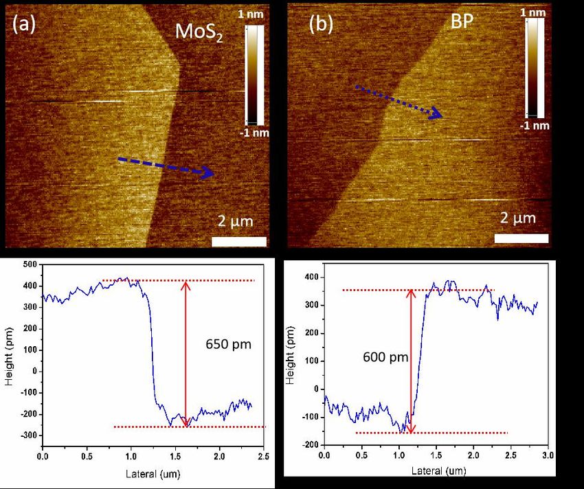
transparent (quartz, sapphire; Fig. 2c) and flexible plastic supports (Fig. 2d). The
transparency persists even for thicker (~10 nm) Au/Ti layers although light
transmission slightly decreases. This method can also be applied to CVD-grown
wafer-scale transition-metal dichalcogenides (TMDCs) materials, such as MoS2 (Fig.
2e).

Fig. 2. Mechanical exfoliation of different monolayer materials with macroscopic size. (a)
Schematic of the exfoliation process. (b-d) Optical images of exfoliated MoS2 on SiO2/Si, sapphire,
and plastic film. (e) 2-inch CVD-grown monolayer MoS2 film transferred onto a 4 inch SiO2/Si
substrate. (f-g) Optical images of large exfoliated 2D crystals: BP, FeSe, Fe3GeTe2, RuCl3, PtSe2, PtTe2,
PdTe2 and CrSiTe3. Those exfoliated monolayers highlighted in the red box are, so far, not accessible
using other mechanical exfoliate method. (h) Optical image and Raman spectra of a MoS2/WSe2
heterostructure. (i) Raman and photoluminescence (PL) spectra of suspended monolayer WSe2. (j)
Optical image of suspended WSe2 with different thicknesses (1L to 3L) and a PL intensity map of the
suspended monolayer.

       X-ray photoelectron spectroscopy (XPS) was employed to further investigate the
interaction between MoS2 and Au. Fig. S2d shows an XPS spectrum of exfoliated
                                                   7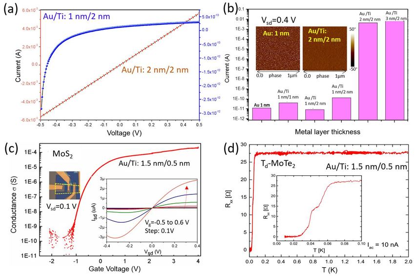
MoS2 near the Mo 3d region. Peaks centered at 226.5 eV, 229 eV, and 232 eV result
from S 2s, Mo 3d5/2 and Mo 3d3/2 photoelectrons, respectively. There are no
appreciable changes in terms of shape, binding energy, and width of the XPS peaks
compared to those of bulk MoS2. Hence, the nearly unchanged XPS spectra confirm
CLQB rather than covalent bonding between MoS2 and the Au substrate. Figs. S3 and
S4 show Raman, photoluminescence (PL) and ARPES of a typical exfoliated MoS2
monolayer. Sharp E2g and A1g Raman peaks at 386 and 406 cm−1, respectively,
confirm the high quality of the MoS2 monolayer34. The pronounced A-exciton PL
peak at 1.83 eV indicates the exfoliated MoS2 on Au is still a direct-band gap
semiconductor35. Metal substrates usually quench the PL intensity of monolayer
MoS223, 24, however, our PL signal remains strong because of the thickness-tunable
conductivity of our metal substrates, as elucidated later.
     We applied the Au-assisted exfoliation method to other 2D crystals and have
obtained a library of 40 large-area single-crystal monolayers, as shown in Fig. 2f-2g
and Fig. S5. Besides transition metal dichalcogenides, the library contains metal
monochalcogenides (e.g., GaS), black phosphorus, black arsenic, metal trichlorides
(e.g., RuCl3) and magnetic compounds (e.g., Fe3GeTe2). It is rather striking that some
monolayers, i.e. FeSe, PdTe2, CrSiTe3, become accessible by our exfoliation method
for the first time. This method is, as we expected according to the smaller RLA/IL
values (1.24 and 1.07), less effective for exfoliating graphene and h-BN monolayers
which are accessible by chemical vapor deposition. The exfoliated monolayer samples
show high quality, as characterized by Raman and atomic force microscopy (Figs. S6
and S7). Reactive samples were exfoliated in a glove box due to their stability issues
in air.
     Our method also promotes preparation of van der Waals heterostructures and
suspended 2D materials at human visible size scales. Fig. 2h shows a typical
monolayer MoS2/WSe2 heterostructure prepared using this method. Raman spectra
(Fig. 2h) show the characteristic vibrational modes of both the MoS2 and WSe2 layers.
Given the exceeding RLA/IL values over 1.3, patterned Au thin-films on substrates with
holes, are also, most likely, able to exfoliate 2D crystals and thus to fabricate
                                            8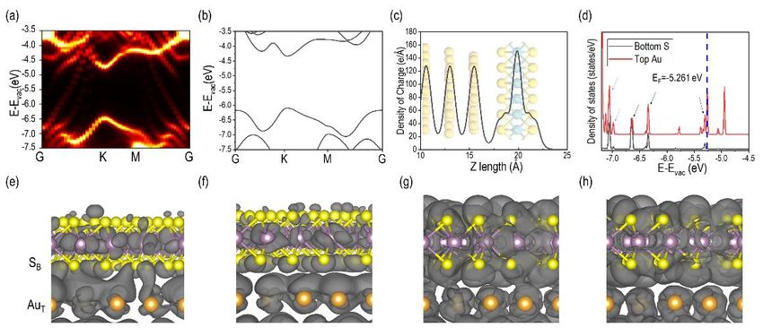
suspended monolayers, which is of paramount importance on studying intrinsic
properties of 2D layers36, 37. We show an example with suspended 1L-3L WSe2 in (Fig.
2i), which can reach 90% coverage over at least tens of micrometers (Fig. S8). The
suspended monolayer film is detached from multilayer instead of transferring
monolayer by organic films, which totally avoid polymer contamination. In
comparison with supported samples on SiO2, the suspended WSe2 (Fig. 2i) shows
enhanced PL intensity (16 times) and sharper PL peak (full width at half maximum
(FWHM): 34 meV, compared with 64 meV for supported WSe2) as shown in Fig. S9.
Since PL can be fully quenched on thicker metal film while well maintained on
suspended area, therefore, we realized patterning of PL even on one monolayer flake
(Fig. 2j).
Fig. 3. STM and ARPES measurements of 2D materials exfoliated onto conductive Au/Ti
adhesion layers. (a) and (b) STM images of monolayer WSe2 and Td-MoTe2, respectively. (c) LEED
pattern of monolayer Td-MoTe2. (d), (e) Band structure of monolayer WSe2. (d) Original ARPES band
structure of monolayer WSe2 (hv = 21.2 eV) along -K high symmetry line. The valence band
maximum (VBM) is positioned at K instead of , which is an important signature of monolayer WSe2.
(e) Second-derivative spectra of band dispersion along K-M-K', showing clear spin-orbital coupling
(SOC) induced spin-splitting bands.
High-quality macroscopic monolayers have practical advantages, for instance in
establishing the lattice structure and electronic band structure of unexplored 2D
materials or van der Waals stacks by scanning tunneling microscopy (STM) and
ARPES. The Au-coated support facilitates such electron-based spectroscopy by
eliminating charging effects associated with insulating (e.g., SiO2) substrates while
9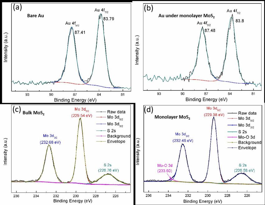
preserving the intrinsic electronic band structures. Figs. 3a and 3b illustrate
atomic-resolution STM images for as-exfoliated WSe2 and Td-MoTe2 monolayers,
which are challenging to image on insulating substrates due to charging effects.
Low-energy electron diffraction with millimeter incident electron beam size shows a
single-phase diffraction pattern for MoTe2 (Fig. 3c), indicating that it is a
single-crystal at the millimeter scale. Fig. 3d displays an ARPES map of the
low-energy electronic structure of the WSe2 monolayer, showing clear and sharp
bands. The valence band features a single flat band around and a large band
splitting near K. Along the -K line, one single band starts to split into two
tΓ
spin-resolved bands at Δ , and the valence band maximum at K sits at ~0.6
eV higher than that at . Fig. 3e displays the symmetric band splitting spectra along
K-M-K' arising from strong spin-orbit coupling mainly at the W site in the WSe2
lattice38. These features constitute the critical signatures of band dispersion in
monolayer TMDCs. Here it deserves an emphasis on the big advantage of large area
of monolayer TMDCs, which make it quite feasible and easy to accurately measure
the band structure by using standard ARPES technique39.
Fig. 4. Electrical measurements of metal adhesion layers and of 2D materials exfoliated onto
non-conductive metal films. (a) Electrical transfer curves of typical Au/Ti adhesion layers. (b)
Two-terminal resistance of Au/Ti layers with different nominal thickness. The inset shows AFM phase
maps of two metal layers. (c) Gate voltage-conductance transfer characteristics of a top-gated MoS2
10FET on SiO2/Si with Au (1.5 nm)/Ti (0.5 nm) adhesion layer (T = 220 K, source−drain bias Vsd= 0.1 V).
Left inset: Optical image of the FET device with windows for the ionic liquid top gate. Right inset:
low-bias source-drain current-voltage characteristics for gate voltage -0.5 - 0.6 V. (d)
Temperature-dependent resistance of a Td-MoTe2 flake exfoliated onto SiO2/Si with a 2 nm metal
adhesion layer.
Even some previous studies claimed to exfoliate large area chalcogenides layers
using gold films22-24, however, further characterizations including optical and
electrical measurements are usually achieved by an additional transfer process onto
insulating substrate. Nevertheless, we show here that the conductivity of Au/Ti
adhesion layer can be drastically tuned by controlling its nominal thickness, which
demonstrate that both optical measurements and device fabrication can be realized on
this one-step exfoliated samples. Fig. 4a and 4b show that the Au/Ti films become
insulating (i.e., electrically discontinuous) if the combined thickness of Ti/Au
decreases to 3 nm or below40. Our exfoliation method is not apparently limited by the
Au thickness, therefore, those large-area 2D crystals are expected to be exfoliated by
either conducting or non-conducting Au coated substrates.
Fig. S3c shows a MoS2 flake exfoliated by an electrically discontinuous (0.5 nm
Ti, 1.5 nm Au) adhesion layer on a SiO2/Si substrate (Fig. 4b inset and Fig. S10), in
which almost no lateral channel is available to carry current flow through the
substrate. Although some prior studies used Au films to enhance exfoliation of MoS2,
the PL intensity of their MoS2 samples was largely quenched22, 24. By contrast, our
MoS2 monolayer exfoliated using electrically discontinuous metal adhesion layers
show intense PL signals (see Fig. S3). Such electrically discontinuous layers also
allow to fabrication of electronic devices directly from the as-exfoliated 2D
monolayers. Fig. 4c shows the trans-conductance curve of a prototype device, a
field-effect transistor (FET) directly built on an as-exfoliated monolayer MoS2
channel on Au(1.5 nm)/Ti(0.5 nm)/SiO2/Si. Fig. S11 shows the device layout. The
device, controlled by an ionic-liquid top gate, shows a high on-off current ratio (>106
at T = 220 K), comparable to usual MoS2 FETs directly fabricated on SiO2/Si
substrates7, 41. A sub-threshold swing (SS) of 100 mV/dec. was derived, close to the
best values reported in the literature7, 42, 43, ranging from 74 mV/dec. to 410 mV/dec.
11Both results show good performance of the FET directly fabricated on the ultrathin
metal adhesion layer and its potential for further improvements. We extended the
individual FET to an FET array directly built on an exfoliated centimeter-scale
single-crystal MoS2 flake using UV lithography (Fig. S12), indicating great potential
of our new exfoliation method for fabrication of integrated circuit.
Since electrical current is prone to flow through superconducting regions, the
metal adhesion layer does not suppress the transition of an exfoliated layer from its
normal state to its superconducting state. Fig. 4d shows a Td-MoTe2 device, directly
fabricated on a 2 nm metal layer, undergoes a metal-superconductor transition at 70
mK, and reaches the zero-resistance at 30 mK. A second onset, observed at 50 mK, is,
most likely, a result of quantum fluctuation in 2D crystals. A previous study of bulk
Td-MoTe2 showed an onset of superconductivity at 250 mK and zero resistance at a
critical temperature Tc=100 mK44. The difference between bulk and monolayer’s Tc
values may be primarily relevant with reduced dimensionality45.
Our combined results show that exfoliation assisted by an Au adhesion layer with
covalent-like quasi bonding to a layered crystal provides access to an unprecedentedly
broad spectrum of large-area monolayer materials. This method is rather unique,
especially for layered crystals that are difficult to exfoliate using conventional
methods. The versatility of this approach is demonstrated here by using Au adhesion
layers for exfoliation of large 2D sheets from 40 layered materials. The efficient
transfer of most 2D crystals is rationalized by calculations that indicate interaction
energies to Au exceeding the interlayer energy for most layered bulk crystals,
graphene and hexagonal boron nitride being notable exceptions. Characterization of
the large-area exfoliated monolayers flakes demonstrates that the flakes are of high
quality. For research on atomically thin materials, the approach demonstrated here has
immediate implications. The availability of macroscopic (millimeter scale) 2D
materials can support the exploration of the properties of new families of ultrathin
semiconductors, metals, superconductors, topological insulators, ferroelectrics, etc., as
well as engineered van der Waals heterostructures. For applications of 2D materials,
an efficient large-scale layer transfer method could force a paradigm shift. So far,
12exfoliation from bulk crystals has not been deemed technologically scalable. But once
exfoliation becomes so consistent that the size of the resulting 2D layers is limited
only by the dimensions and crystallinity of the source crystal, the focus of
application-driven materials research may shift toward optimizing the growth of
high-quality layered bulk crystals. Ironically, the fabrication of 2D materials for
applications would then follow the well-established and highly successful example of
silicon technology, where the extraction of wafers from large, high-quality single
crystals has long been key to achieving the yields and reliability required for
industrial applications.
13Materials and Methods
DFT calculations: DFT calculations were performed using the generalized gradient
approximation for the exchange-correlation potential, the projector augmented wave method ,
46, 47
and a plane-wave basis set as implemented in the Vienna ab-initio simulation package (VASP) 48.
The energy cutoff for plane wave was set to 700 and 500 eV for variable volume structural
relaxation of pure 2D materials and invariant volume structural relaxation of these materials on Au
(111) surface. Dispersion correction was made at the van der Waals density functional (vdW-DF)
level, with the optB86b functional for the exchange potential49. Seven Au (111) layers, separated
by a 15 Å vacuum surface slab, were employed to model the surface. The four bottom layers were
kept fixed and all other atoms were fully relaxed until the residual force per atom was less than
0.04 eV•Å-1 during the relaxations of 2D materials on the Au (111) surfaces and less than 0.01
eV•Å-1 during all the other structural relaxations. The lattice constancies of Au (111) surface
model were changed to match those of 2D materials for keeping electronic properties of 2D
materials unchanged by strains or stresses. The lattice mismatches between 2D materials and Au
(111) surface were kept lower than 4.5%.
Gold-enhanced mechanical exfoliation: The metal layer deposition was completed in an
electron evaporation system (Peva-600E). An adhesion metal layer (Ti or Cr) was first evaporated
on Si substrate (with 300 nm SiO2 film), after that Au film was deposited on the substrate. The
thickness of Ti (or Cr) and Au can be well controlled by the evaporation rate (0.5 Å/s). After
depositing metal layers on Si wafer, a fresh surface of layered crystal was cleaved from tape and
put it onto the substrate. By pressing the tape vertically for about 1 min, the tape can be removed
from substrate. Large area monolayer flakes can be easily observed by optical microscope or even
by eyes. Most of the time, the size of monolayer flakes is limited by the size of bulk crystal.
Suspended samples preparation: Si wafer with 300 nm SiO2 was patterned by
UV-lithography, after that the hole array structures were prepared by reactive-ion etching. The
diameter and depth of each hole is 5 μm and 10 μm. The metal layers (Au/Ti: 2 nm/2 nm)
deposited on the Si substrate with hole array before exfoliating layered materials on it. Large area
suspended 2D materials can be exfoliated on the hole array substrate.
Characterization and measurement:
14The Raman and PL measurements were performed on a JY Horiba HR800 system with a
wavelength of 532 nm and power at 0.6 mW. Fig. S3 shows the Raman, and PL results of a typical
exfoliated MoS2 film. Raman peaks of E12g and A1g are at 386 and 406 cm−1, respectively. From
the Raman result, we can determine the following: first, the space between the two peaks (Δ) is
~20 cm−1, suggesting that the as-exfoliated material is monolayer; second, the Raman peaks show
no split, suggesting that the crystal quality of the as-grown MoS2 film is good. The PL peak of A
exciton is at 1.83 eV. These features are in good agreement with the data seen previously for
monolayer MoS2.
Fig. S6 presents the representative Raman spectra for monolayer and few-layer BP and
α-RuCl3 samples excited by 2.33 eV radiation in vacuum environments. The laser power on the
sample during Raman measurement was kept below 100 μW in order to avoid sample damage and
excessive heating. The silicon Raman mode at 520.7 cm-1 was used for calibration prior to
measurements and as an internal frequency reference.
In close analogy to bulk, three typical Raman peaks are resolved at 360, 436, and 465 cm-1 for
monolayer and few-layer BP samples. It can be seen that the phonon intensity decreases with layer
numbers. The evolution of Raman intensity versus the number of layers is attributed to the
multilayer interference occurring for both the incident light and the emitted Raman radiation,
being akin to the case of graphene50 and MoS251, 52.
As for monolayer and few-layer α-RuCl3 samples, five strong and sharp phonon modes are
resolved at 117, 164, 270, 296 and 312 cm-1. It should be noted that the two lowest energy
phonons in α-RuCl3 show asymmetric Fano line shape stemmed from the coupling between the
discrete optical phonons and the magnetic scattering, as we have discussed before53.
For all thicknesses, it can be seen that the energies of all phonons are independent on the
number of layers, as indicated by the dashed vertical lines in Fig. S6. This is in marked contrast to
TMDC33 and indicates that the van der Waals interlayer interactions in BP and α-RuCl3 are
extremely weak and have tiny effects on phonon energy.
The atomic force microscope (AFM) scanning (Veeco Multimode III) was used to check the
thickness and surface morphology of those monolayer samples. Fig. S7 shows the AFM images of
atomically thin MoS2 and BP flakes. Judging from the morphology of the freshly exfoliated
samples at the nanometer scale, there is no evidence of structural irregularity or bubbles on the
15surfaces. The height profiles taken along the blue lines in AFM images are depicted below. It is
noted that the height of monolayer MoS2/BP on SiO2/Si substrate is about ~0.65 nm/~0.6 nm, a
little larger than the theoretical thickness. The deviation implies that there are some absorbents at
the interface between the MoS2/BP and SiO2/Si substrate51, 54.
The X-ray photoelectron spectroscopy (XPS, Thermo Scientific ESCALAB 250 Xi) was
performed with Al Kα X-rays (hυ = 1486.6 eV) in an analysis chamber that had a base
pressure < 3 × 10⁻⁹ Torr. Core spectra were recorded using a 50 eV constant pass energy (PE) in
50-100 μm small area lens mode (i.e., aperture selected area). The XPS peaks were calibrated
using the adventitious carbon C1s peak position (284.8 eV). XPS analysis was employed to obtain
the core-level XPS spectra for the comparison of exfoliated single layer MoS2 and bulk MoS2
flakes (Fig. S2). The high-resolution spectra and the fitting curves of Au 4f peaks in Fig. S4a, b do
not show noticeable difference of the binding energies but with a slightly decreased intensity for
the Au spectra under MoS2 flake due to the screening effect. While the core-level Mo 3d and S 2s
spectra of the exfoliated MoS2 show a small redshift (around 0.2 eV) when compared with the
bulk MoS2 bulk flakes, suggesting a possible charge transfer between the single layer MoS2 flake
and the underlying Au film22, 55. In addition, the consistence of the shape and peak width of the
Mo 3d spectra of the exfoliated single layer MoS2 with the bulk MoS2 flake indicates that the
single layer MoS2 is clean and retains its chemical identity after exfoliation. This XPS result
demonstrates the important role of Au for the successful exfoliation of large single layer MoS2
flake.
The scanning tunneling microscope (STM) measurement was performed using a custom built,
low-temperature, and UHV STM system at 300 K. A chemically etched W STM tip was cleaned
and calibrated against a gold (111) single crystal prior to the measurements.
High resolution angle-resolved photoemission spectroscopy (ARPES) measurements were
carried out on our lab system equipped with a Scienta R4000 electron energy analyzer56. We use
Helium discharge lamp as the light source which can provide photon energies of hυ = 21.218 eV
(Helium I). The energy resolution was set at 10~20 meV for band structure measurements (Fig. 3).
The angular resolution is ~0.3 degree. The Fermi level is referenced by measuring on a clean
polycrystalline gold that is electrically connected to the sample. The samples were measured in
vacuum with a base pressure better than 5×10-11 Torr.
16The electrical characteristic measurements were carried out in the probe station with the
semiconductor parameter analyzers (Agilent 4156C and B1500) and oscilloscope.
Online Content
Methods, along with any additional Extended Data display items and Source Data, are
available in the online version of the paper; references unique to these sections appear
only in the online paper.
17Acknowledgments
This work is supported by the National Key Research and Development Program of
China (Grant No. 2019YFA0308000, 2018YFA0305800, 2018YFE0202700), the
Youth Innovation Promotion Association of CAS (2019007, 2018013), the National
Natural Science Foundation of China (Grant No. 11874405, 11622437, 61674171 and
11974422), the National Basic Research Program of China (Grant No.
2015CB921300), and the Strategic Priority Research Program (B) of the Chinese
Academy of Sciences (Grant No. XDB07020300, XDB30000000), the Research
Program of Beijing Academy of Quantum Information Sciences (Grant No. Y18G06).
P.S. and E.S. acknowledge support by the U.S. Department of Energy, Office of
Science, Basic Energy Sciences, under Award No. DE-SC0016343. Calculations were
performed at the Physics Lab of High-Performance Computing of Renmin University
of China and Shanghai Supercomputer Center.
Author Contributions
P.S., W.J., H.J.G. and X.J.Z. are equally responsible for supervising the discovery. Y.H.
and R.Y. conceived the project. Y.H.P., J.P.H. and J.W. performed the DFT
calculations. Y.H., H.L.L and L.L. prepared all the mechanical exfoliation samples.
Y.H. and R.Y. performed the Raman, PL and AFM measurements. M.H., J.W., P.S.
and E.S. performed XPS measurement. Y.Q.C., G.D.L., L.Z. and W.J.Z. performed the
ARPES measurement. Z.L.Z., P.C., K.H.W., L.M., Z.Z. and Y.L.W performed the
STM and LEED measurement. Y.G.S. and Y.F.G. prepared bulk layered crystals.
S.B.T., C.Z.G., Z.G.C., L.M.W. and L.H.B. fabricated the transistors and performed
the electrical measurements. Y.H., R.Y., J.P.H., P.S., and W.J. analyzed data, wrote the
manuscript and all authors discussed and commented on it. These authors contributed
equally: Y.H, Y.H.P and R.Y.
Competing interests
Three Chinese patents were filed (DIC19110040, DIC19110039 and DIC19110044)
by the Institute of Physics, Chinese Academy of Sciences, along with their researchers
(Y.H., H.L.L and X.J.Z).
18References
1. He, S.L. et al. Phase diagram and electronic indication of high-temperature superconductivity
at 65 K in single-layer FeSe films. Nature Materials 12, 605-610 (2013).
2. Chen, G.R. et al. Evidence of a gate-tunable Mott insulator in a trilayer graphene moire
superlattice. Nature Physics 15, 237-241 (2019).
3. Ezawa, M. Valley-Polarized Metals and Quantum Anomalous Hall Effect in Silicene. Physical
Review Letters 109, 055502 (2012).
4. Jiang, S.W., Li, L.Z., Wang, Z.F., Mak, K.F. & Shan, J. Controlling magnetism in 2D CrI3 by
electrostatic doping. Nature Nanotechnology 13, 549-553 (2018).
5. Novoselov, K.S. et al. Electric field effect in atomically thin carbon films. Science 306,
666-669 (2004).
6. Huang, Y. et al. Reliable Exfoliation of Large-Area High-Quality Flakes of Graphene and
Other Two-Dimensional Materials. Acs Nano 9, 10612-10620 (2015).
7. Radisavljevic, B., Radenovic, A., Brivio, J., Giacometti, V. & Kis, A. Single-layer MoS2
transistors. Nature Nanotechnology 6, 147-150 (2011).
8. McGuire, M.A., Dixit, H., Cooper, V.R. & Sales, B.C. Coupling of Crystal Structure and
Magnetism in the Layered, Ferromagnetic Insulator CrI3. Chemistry of Materials 27, 612-620
(2015).
9. Jiang, D. et al. High-T-c superconductivity in ultrathin Bi2Sr2CaCu2O8+x down to half-unit-cell
thickness by protection with graphene. Nature Communications 5 (2014).
10. Tang, S.J. et al. Quantum spin Hall state in monolayer 1T '-WTe2. Nature Physics 13, 683-687
(2017).
11. Zhang, Y. et al. Superconducting Gap Anisotropy in Monolayer FeSe Thin Film. Physical
Review Letters 117, 117001 (2016).
12. Novoselov, K.S., Mishchenko, A., Carvalho, A. & Neto, A.H.C. 2D materials and van der
Waals heterostructures. Science 353, 9439 (2016).
13. Liu, Y. et al. Van der Waals heterostructures and devices. Nature Reviews Materials 1 (2016).
14. Wang, C. et al. Monolayer atomic crystal molecular superlattices. Nature 555, 231-236 (2018).
15. Li, X.S., Cai, W.W., Colombo, L. & Ruoff, R.S. Evolution of Graphene Growth on Ni and Cu
by Carbon Isotope Labeling. Nano Letters 9, 4268-4272 (2009).
16. Moon, I.K., Lee, J., Ruoff, R.S. & Lee, H. Reduced graphene oxide by chemical graphitization.
Nature Communications 1, 73 (2010).
17. Sutter, P.W., Flege, J.I. & Sutter, E.A. Epitaxial graphene on ruthenium. Nature Materials 7,
406-411 (2008).
18. Meng, L. et al. Buckled Silicene Formation on Ir(111). Nano Letters 13, 685-690 (2013).
19. Liu, H., Du, Y.C., Deng, Y.X. & Ye, P.D. Semiconducting black phosphorus: synthesis,
transport properties and electronic applications. Chemical Society Reviews 44, 2732-2743
(2015).
20. Coleman, J.N. et al. Two-Dimensional Nanosheets Produced by Liquid Exfoliation of Layered
Materials. Science 331, 568-571 (2011).
21. Fan, X.B. et al. Fast and Efficient Preparation of Exfoliated 2H MoS2 Nanosheets by
Sonication-Assisted Lithium Intercalation and Infrared Laser-Induced 1T to 2H Phase
Reversion. Nano Letters 15, 5956-5960 (2015).
22. Desai, S.B. et al. Gold-Mediated Exfoliation of Ultralarge Optoelectronically-Perfect
19Monolayers. Advanced Materials 28, 4053-4058 (2016).
23. Velicky, M. et al. Mechanism of Gold-Assisted Exfoliation of Centimeter-Sized
Transition-Metal Dichalcogenide Monolayers. ACS Nano 12, 10463-10472 (2018).
24. Magda, G.Z. et al. Exfoliation of large-area transition metal chalcogenide single layers.
Scientific Reports 5 (2015).
25. Zhang, Y.B., Tan, Y.W., Stormer, H.L. & Kim, P. Experimental observation of the quantum
Hall effect and Berry's phase in graphene. Nature 438, 201-204 (2005).
26. Novoselov, K.S. et al. Two-dimensional gas of massless Dirac fermions in graphene. Nature
438, 197-200 (2005).
27. Cao, Y. et al. Unconventional superconductivity in magic-angle graphene superlattices. Nature
556, 43-50 (2018).
28. Hao, Y.F. et al. Oxygen-activated growth and bandgap tunability of large single-crystal bilayer
graphene. Nature Nanotechnology 11, 426-431 (2016).
29. Qiao, J.S., Kong, X.H., Hu, Z.X., Yang, F. & Ji, W. High-mobility transport anisotropy and
linear dichroism in few-layer black phosphorus. Nature Communications 5, 4475 (2014).
30. Hu, Z.-X., Kong, X., Qiao, J., Normand, B. & Ji, W. Interlayer electronic hybridization leads
to exceptional thickness-dependent vibrational properties in few-layer black phosphorus.
Nanoscale 8, 2740-2750 (2016).
31. Qiao, J. et al. Few-layer Tellurium: one-dimensional-like layered elementary semiconductor
with striking physical properties. Science Bulletin 63, 159-168 (2018).
32. Li, W. et al. Experimental realization of honeycomb borophene. Science Bulletin 63, 282-286
(2018).
33. Deng, Y. et al. Gate-tunable room-temperature ferromagnetism in two-dimensional Fe3GeTe2.
Nature 563, 94-99 (2018).
34. Li, H. et al. From Bulk to Monolayer MoS2: Evolution of Raman Scattering. Advanced
Functional Materials 22, 1385-1390 (2012).
35. Mak, K.F., Lee, C., Hone, J., Shan, J. & Heinz, T.F. Atomically Thin MoS2: A New Direct-Gap
Semiconductor. Physical Review Letters 105, 136805 (2010).
36. Du, X., Skachko, I., Barker, A. & Andrei, E.Y. Approaching ballistic transport in suspended
graphene. Nature Nanotechnology 3, 491-495 (2008).
37. Lee, C., Wei, X.D., Kysar, J.W. & Hone, J. Measurement of the elastic properties and intrinsic
strength of monolayer graphene. Science 321, 385-388 (2008).
38. Zhang, Y. et al. Electronic Structure, Surface Doping, and Optical Response in Epitaxial WSe2
Thin Films. Nano Letters 16, 2485-2491 (2016).
39. Zhang, H.Y. et al. Resolving Deep Quantum-Well States in Atomically Thin 2H-MoTe2 Flakes
by Nanospot Angle-Resolved Photoemission Spectroscopy. Nano Letters 18, 4664-4668
(2018).
40. Frydendahl, C. et al. Optical reconfiguration and polarization control in semi-continuous gold
films close to the percolation threshold. Nanoscale 9, 12014-12024 (2017).
41. Yoon, Y., Ganapathi, K. & Salahuddin, S. How Good Can Monolayer MoS2 Transistors Be?
Nano Letters 11, 3768-3773 (2011).
42. Liu, W., Sarkar, D., Kang, J.H., Cao, W. & Banerjee, K. Impact of Contact on the Operation
and Performance of Back-Gated Monolayer MoS2 Field-Effect-Transistors. ACS Nano 9,
7904-7912 (2015).
2043. Kappera, R. et al. Phase-engineered low-resistance contacts for ultrathin MoS2 transistors.
Nature Materials 13, 1128-1134 (2014).
44. Qi, Y.P. et al. Superconductivity in Weyl semimetal candidate MoTe2. Nature Communications
7, 11038 (2016).
45. Xi, X. et al. Ising pairing in superconducting NbSe2 atomic layers. Nature Physics 12,
139-143 (2016).
46. Blochl, P.E. Projector Augmented-Wave Method. Physical Review B 50, 17953-17979 (1994).
47. Kresse, G. & Joubert, D. From ultrasoft pseudopotentials to the projector augmented-wave
method. Physical Review B 59, 1758-1775 (1999).
48. Kresse, G. & Furthmuller, J. Efficient iterative schemes for ab initio total-energy calculations
using a plane-wave basis set. Physical Review B 54, 11169-11186 (1996).
49. Klimes, J., Bowler, D.R. & Michaelides, A. Van der Waals density functionals applied to
solids. Physical Review B 83, 195131 (2011).
50. Ferrari, A.C. et al. Raman spectrum of graphene and graphene layers. Physical Review Letters
97, 187401 (2006).
51. Lee, C. et al. Anomalous Lattice Vibrations of Single- and Few-Layer MoS2. ACS Nano 4,
2695-2700 (2010).
52. Zhang, H. et al. Interference effect on optical signals of monolayer MoS2. Applied Physics
Letters 107, 101904 (2015).
53. Du, L.J. et al. 2D proximate quantum spin liquid state in atomic-thin alpha-RuCl3. 2D
Materials 6, 015014 (2019).
54. Zhou, B.Y. et al. Possible structural transformation and enhanced magnetic fluctuations in
exfoliated alpha-RuCl3. Journal of Physics and Chemistry of Solids 128, 291-295 (2019).
55. Shi, J.P. et al. Monolayer MoS2 Growth on Au Foils and On-Site Domain Boundary Imaging.
Advanced Functional Materials 25, 842-849 (2015).
56. Liu, G.D. et al. Development of a vacuum ultraviolet laser-based angle-resolved
photoemission system with a superhigh energy resolution better than 1 meV. Review of
Scientific Instruments 79, 023105 (2008).
21Supplementary Information for
Universal mechanical exfoliation of large-area 2D crystals
Yuan Huang†, Yu-Hao Pan†, Rong Yang†, Li-Hong Bao, Lei Meng, Hai-Lan Luo,
Yong-Qing Cai, Guo-Dong Liu, Wen-Juan Zhao, Zhang Zhou, Liang-Mei Wu, Zhi-Li
Zhu, Ming Huang, Li-Wei Liu, Lei Liu, Peng Cheng, Ke-Hui Wu, Shi-Bing Tian,
Chang-Zhi Gu, You-Guo Shi, Yan-Feng Guo, Zhi Gang Cheng, Jiang-Ping Hu, Lin
Zhao, Eli Sutter, Peter Sutter*, Ye-Liang Wang, Wei Ji*, Xing-Jiang Zhou*, and
Hong-Jun Gao*
†
These authors contributed equally to this work.
*Correspondence to: psutter@unl.edu (P.S.); wji@ruc.edu.cn (W.J.); xjzhou@iphy.ac.cn (X.J.Z.);
hjgao@iphy.ac.cn (H.J.G.)
22Fig. S1. Electronic structures of an Au (111) supported monolayer MoS2
(1L-MoS2), a typical 2D material, interface. Here, MoS2 was chosen in
consideration of that it has a moderate RLA/IL of 1.51 and group 16 (VIA) elements are
the major portion of non-metal elements in all considered 2D layers. The vacuum
energy was set as energy zero in both bandstructures and DOS plots. (a) Unfolded
bandstructure of the interface, which was calculated using the KPROJ program based
on the k-projection method1,2. (b) Bandstructure of freestanding 1L-MoS2. The
bandgap of 1.76 eV and the shape of valence (VB) and conduction (CB) bands remain
nearly unchanged after the free-standing layer in contact with the Au substrate while
the positions of VB and CB shift downward by ~0.5 eV. This shift is a result of
vertical electric dipole moments (~0.75 e·Å) formed at the interface upon contact,
which were illustrated by the DCD in Fig. 1e and a layer-averaged line profile
associated with total electronic charge density, as plotted in (c). Dipole moment p here
is defined as , where e is the electron charge, the
summation is over Mo and S ionic sites, and is the electronic charge density in
the MoS2 interlayer. Both VB and CB of the intact MoS2 were perturbed by some Au
states, as depicted in (a), which indicates Au states electronically hybridize with states
of MoS2. We plotted local density of states (LDOS) of the interface in (d) in order to
reveal the interactions between MoS2 and Au (111). Only the Gamma point was used
for clarity. Grey and red lines represent the LDOSs of an interfacial S atom (denote SB)
and an interfacial Au atom (denote AuT). The hybrid states of SB and AuT were
marked by black and light blue arrows. Each of those peaks contains six states while
some of those states were representatively visualized in (e) to (h). Panels (e) and (f)
plot the isosurface contours of wavefunction norms for the bonding and anti-bonding
states sitting at ~ -5.3 eV with an isosurface value of 1×10⁻⁴ e/Bohr3, while those for
the states at ~ -7.0 eV were shown in (g) and (h) with an isosurface value of 3×10⁻⁵
e/Bohr3, respectively. The hybridization between them, however, is not as strong as a
covalent bond. The energy splitting of bonding-states and anti-bonding states is only
few meV for those states marked by the black arrows and is up to 86 meV for those
states marked by the light-blue arrows. While both the bonding and anti-bonding
states all fully occupied, together with the rather small energy splitting, we conclude
the interaction between Au and MoS2 is not covalent bonding, but an interaction type
23called covalent-like quasi-bonding (CLQB), as we discussed in the main text and
recently identified in 2D layers.
Fig. S2. (a, b) XPS spectra of Au 4f from bare Au surface and the Au beneath a
monolayer MoS2 flake. (c, d) Mo 3d and S 2s spectra and the corresponding fitting
curves of a bulk MoS2 flake and of an exfoliated single layer MoS2 flake.
24Fig. S3. Raman and PL spectra of MoS2 exfoliated with Au/Ti adhesion layer
(nominally 1.5 nm/0.5 nm). (a) Raman spectra of monolayer and bilayer MoS2,
normalized by the intensity of the Si peak at 520 cm-1. (b) PL spectrum of monolayer
MoS2 exfoliated onto the ultrathin Au/Ti adhesion layer. (c) Optical image of a MoS2
flake with coexisting monolayer and few-layer areas. (d) PL mapping image of the
MoS2 flake shown in (c), with PL intensity in the monolayer area substantially higher
than in few-layer and substrate regions.
25Fig. S4. Band structure of monolayer MoS2 flake exfoliated on Au/Ti adhesion layer
(5 nm/1 nm).
Fig. S5. Optical images of 2D materials exfoliated using Au adhesion layers. Some of
materials shown are obtained here for the first time in monolayer form, for example,
IrTe2, ZrTe3, PtSe2. Scale bars: 500 μm.
26Fig. S6. Raman spectra of exfoliated black phosphorus (BP) and RuCl3 crystals with
different thickness, in comparison with the corresponding layered bulk crystals.
Fig. S7. AFM images of as-exfoliated 2D MoS2 and black phosphorus/phosphorene
(BP).
27Fig. S8. Suspended WSe2 samples with suspended coverage of 97% and 93%,
respectively.
Fig. S9. Raman and PL spectra of suspended monolayer WSe2 in comparison with
monolayer WSe2 supported on a SiO2/Si substrate.
28Fig. S10. AFM images of Au/Ti (1.5 nm/ 0.5 nm) adhesion layers before and after
annealing (250 0C, 2h).
Fig. S11. (a) Monolayer field-effect transistor (FET) device structure with ionic liquid
top gate. (b) Optical micrograph of an actual FET device with monolayer MoS2
channel, and an insulating PMMA coating with window for the ionic liquid top gate.
29Fig. S12. Optical image of UV-patterned MoS2 device arrays fabricated from a single
large monolayer MoS2 flake exfoliated onto an ultrathin Au/Ti adhesion layer.
30Table S1. Calculated energies of all 58 considered 2D materials
Ads.
Ads. Interlayer Interlayer
Ads. Interlayer Energy on
Energy on Coupling Coupling
Energy on Coupling Au(111) Magnetic
2D-Materials Au(111) Energy Energy (eV)/ RLA/IL Space Group
Au(111) Energy (eV)/ Structure*
(eV)/unit (eV)/unit Bottom
(eV)/Å2 (eV)/Å2 Bottom
cell cell Atom
Atom
h-BN 0.146 0.136 0.0268 0.0250 0.073 0.068 1.07 P -6 m 2 NM
Gr 0.147 0.118 0.0279 0.0225 0.073 0.059 1.24 P 63/m m c NM
P(Black) 0.801 0.484 0.0556 0.0334 0.400 0.242 1.67 Cmca NM
As(Black) 1.014 0.584 0.0597 0.0350 0.507 0.292 1.71 Cmca NM
W2N3 0.520 0.230 0.0716 0.0316 0.520 0.230 2.26 P 63/m m c NM
TiS2 1.087 0.542 0.0547 0.0273 0.543 0.271 2.00 P -3 m 1 NM
VS2 0.412 0.265 0.0476 0.0305 0.412 0.265 1.56 P -3 m 1 FM
NbS2 0.605 0.264 0.0632 0.0276 0.605 0.264 2.29 R3mH NM
TaS2-2H 0.549 0.249 0.0575 0.0262 0.549 0.249 2.19 P 63/m m c NM
TaS2-1T 0.457 0.278 0.0469 0.0286 0.457 0.278 1.64 P -3 m 1 NM
MoS2 0.345 0.229 0.0397 0.0263 0.345 0.229 1.51 P 63/m m c NM
WS2 0.329 0.227 0.0371 0.0261 0.329 0.227 1.42 P 63/m m c NM
ReS2 1.128 0.856 0.0312 0.0211 0.282 0.214 1.48 P -1 NM
CoPS3 4.883 1.433 0.0829 0.0211 1.221 0.358 3.35 C1 2/m 1 FM
NiPS3 1.946 1.354 0.0336 0.0233 0.486 0.339 1.44 C1 2/m 1 FM
PdS2 1.479 0.889 0.0494 0.0290 0.739 0.445 1.71 Pbca NM
PtS2 0.457 0.292 0.0421 0.0262 0.457 0.292 1.60 P -3 m 1 NM
GaS 0.388 0.218 0.0347 0.0196 0.194 0.109 1.78 P 63/m m c NM
InS 1.093 1.025 0.0718 0.0588 0.547 0.512 1.22 Pmnn NM
GeS2 0.316 0.273 0.0262 0.0223 0.316 0.273 1.17 P 42/n m c Z NM
SnS 0.90 0.617 0.0534 0.0365 0.451 0.309 1.46 Pnma NM
SnS2 0.488 0.243 0.0418 0.0207 0.488 0.243 2.02 P -3 m 1 NM
TiSe2 0.483 0.289 0.0454 0.0270 0.483 0.289 1.68 P -3 m 1 NM
VSe2 0.476 0.261 0.0502 0.0272 0.476 0.261 1.85 P -3 m 1 FM
NbSe2 0.607 0.304 0.0590 0.0295 0.607 0.304 2.00 P 63/m m c NM
MoSe2 0.414 0.243 0.0441 0.0258 0.414 0.243 1.71 P 63/m m c NM
WSe2 0.384 0.241 0.0409 0.0256 0.384 0.241 1.60 P 63/m m c NM
ReSe2 1.458 0.906 0.0373 0.0232 0.364 0.227 1.61 P -1 NM
FeSe 0.565 0.381 0.0424 0.0285 0.565 0.381 1.49 Cmma AFM
PdSe2 1.284 1.117 0.0388 0.0288 0.642 0.559 1.34 Pbca NM
PtSe2 0.641 0.341 0.0537 0.0276 0.641 0.341 1.95 P -3 m 1 NM
GaSe 0.352 0.228 0.0285 0.0185 0.176 0.114 1.54 P 63/m m c NM
InSe 0.519 0.267 0.0369 0.0188 0.259 0.133 1.97 P 63/m m c NM
GeSe2 0.411 0.335 0.0304 0.0242 0.411 0.335 1.25 P 42/n m c Z NM
SnSe 1.033 0.658 0.0560 0.0353 0.516 0.329 1.58 Pnma NM
SnSe2 0.621 0.275 0.0488 0.0214 0.621 0.275 2.24 P -3 m 1 NM
Sb2Se3 0.630 0.340 0.0448 0.0239 0.630 0.340 1.88 R -3 m H NM
31Bi2Se3 0.618 0.336 0.0416 0.0224 0.618 0.336 1.86 R -3 m H NM
ZrTe3 1.283 0.633 0.0554 0.0274 0.428 0.211 2.02 P1 21m/m 1 NM
ZrTe5 2.378 1.088 0.0431 0.0186 1.189 0.544 2.32 Cmcm NM
HfTe3 1.307 0.637 0.0567 0.0279 0.436 0.212 2.03 P1 21m/m 1 NM
HfTe5 1.538 1.078 0.0280 0.0186 0.308 0.216 1.51 Cmcm NM
VTe2 0.658 0.295 0.0585 0.0262 0.658 0.295 2.23 P -3 m 1 FM
MoTe2 0.490 0.281 0.0456 0.0261 0.490 0.281 1.75 P 63/m m c NM
WTe2 1.026 0.516 0.0471 0.0235 0.513 0.258 2.00 P m n 21 NM
MnBi2Te4 0.791 0.368 0.0497 0.0229 0.791 0.368 2.17 R -3 m H FM
FeTe 0.654 0.329 0.0461 0.0232 0.654 0.329 1.99 Cmma AFM
IrTe2 0.870 0.683 0.0680 0.0503 0.870 0.683 1.35 P -3 m 1 NM
PtTe2 0.865 0.479 0.0631 0.0334 0.865 0.479 1.89 P -3 m 1 NM
Sb2Te3 0.773 0.404 0.0489 0.0256 0.773 0.404 1.91 R -3 m H NM
Bi2Te3 0.842 0.397 0.0508 0.0235 0.842 0.397 2.16 R -3 m H NM
CrCl3 0.800 0.550 0.0300 0.0180 0.267 0.183 1.67 R -3 H FM
RuCl3 1.111 0.574 0.0356 0.0184 0.370 0.191 1.94 P 31 1 2 AFM
CdCl2 0.260 0.203 0.0204 0.0158 0.260 0.203 1.29 R -3 m H NM
CrBr3 1.693 1.207 0.0245 0.0175 0.282 0.201 1.40 R -3 H FM
CdBr2 0.323 0.222 0.0234 0.0160 0.323 0.222 1.47 R -3 m H NM
CrI3 1.425 0.715 0.0344 0.0175 0.475 0.119 1.96 R -3 H FM
CdI2 0.387 0.247 0.0248 0.0157 0.387 0.247 1.57 R -3 m H NM
NM: Non-magnetic; FM: Ferromagnetic; AFM: Antiferromagnetic
*
Reference:
1 Mingxing Chen* and M. Weinert, Layer k-projection and unfolding electronic bands at
interfaces, Phys. Rev. B 98, 245421 (2018).
2 M. X. Chen*, W. Chen, Zhenyu Zhang and M. Weinert, Effects of magnetic dopants in
(Li0.8M0.2OH)FeSe (M = Fe, Mn, Co): Density functional theory study using a band unfolding
technique, Phys. Rev. B 96, 245111 (2017).
32You can also read