UCLA UCLA Electronic Theses and Dissertations - eScholarship
←
→
Page content transcription
If your browser does not render page correctly, please read the page content below
UCLA
UCLA Electronic Theses and Dissertations

Title
An RF Receiver Architecture for Intra-Band Carrier Aggregation

Permalink
https://escholarship.org/uc/item/5mr5j64k

Author
Hwu, Sy-Chyuan

Publication Date
2013

Peer reviewed|Thesis/dissertation

 eScholarship.org                              Powered by the California Digital Library
                                                               University of California
University of California
                    Los Angeles

   An RF Receiver Architecture
for Intra-Band Carrier Aggregation

   A dissertation submitted in partial satisfaction
         of the requirements for the degree
   Doctor of Philosophy in Electrical Engineering

                         by

               Sy-Chyuan Hwu

                        2013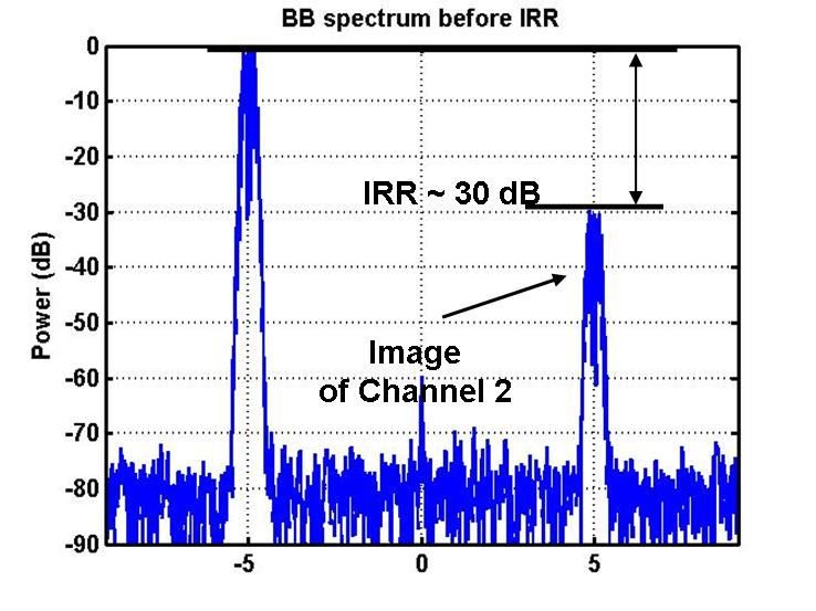
c Copyright by
Sy-Chyuan Hwu
    2013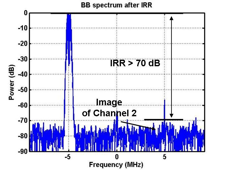
Abstract of the Dissertation

              An RF Receiver Architecture
           for Intra-Band Carrier Aggregation
                                        by

                              Sy-Chyuan Hwu
                 Doctor of Philosophy in Electrical Engineering
                   University of California, Los Angeles, 2013
                          Professor Behzad Razavi, Chair

Carrier aggregation is an attractive approach to increasing the data rate in wire-
less communication. The basic idea is to transmit and receive data on two (or
more) different carriers, thus raising the data rate proportionally. For exam-
ple, Release 10 of the LTE mobile phone standard supports both intra-band and
inter-band aggregation.

   A receiver supporting several carriers may simply employ multiple signal paths
and corresponding frequency synthesizers but at the cost of high power and ex-
tremely stringent isolation requirements among the local oscillators.

   This research introduces an efficient carrier aggregation receiver architecture
that employs one receive path and a single synthesizer. The block-downconversion
scalable receiver translates all of the channels to the baseband and utilizes a new
digital image rejection technique to reconstruct the signals.

   A receiver prototype realized in 45-nm CMOS technology along with an FPGA
back end provides an image rejection ratio of at least 70 dB across the entire band
with a noise figure of 3.8 dB while consuming 15 mW, a factor of four less than

                                        ii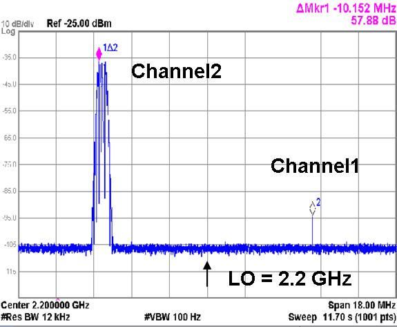
the prior art.

                 iii
The dissertation of Sy-Chyuan Hwu is approved.
Milos Ercegovac
Frank M.-C. Chang
Behzad Razavi, Committee Chair
University of California, Los Angeles
2013
ivTo my wife, my family and my son . . .
vTable of Contents
1 Introduction . . . . . . . . . . . . . . . . . . . . . . . . . . . . . . . . 1
2 Background . . . . . . . . . . . . . . . . . . . . . . . . . . . . . . . . 3
2.1 LTE Specifications . . . . . . . . . . . . . . . . . . . . . . . . . . 3
2.2 Prior Art . . . . . . . . . . . . . . . . . . . . . . . . . . . . . . . 5
3 Proposed Receiver Architecture . . . . . . . . . . . . . . . . . . . 9
4 Proposed Image Rejection Algorithm . . . . . . . . . . . . . . . . 11
4.1 Frequency-Dependent I/Q Mismatch . . . . . . . . . . . . . . . . 11
4.2 Proposed Algorithm . . . . . . . . . . . . . . . . . . . . . . . . . 15
4.3 Computation Cost . . . . . . . . . . . . . . . . . . . . . . . . . . 19
5 Receiver Implementation . . . . . . . . . . . . . . . . . . . . . . . . 20
5.1 FPGA Implementation . . . . . . . . . . . . . . . . . . . . . . . . 20
5.2 Receiver Design . . . . . . . . . . . . . . . . . . . . . . . . . . . . 24
6 RF Front End . . . . . . . . . . . . . . . . . . . . . . . . . . . . . . . 26
6.1 Proposed Low-Noise Amplifier . . . . . . . . . . . . . . . . . . . . 26
6.2 LNA Biasing . . . . . . . . . . . . . . . . . . . . . . . . . . . . . 27
6.3 Noise Analysis . . . . . . . . . . . . . . . . . . . . . . . . . . . . . 31
6.4 Noise Figure Comparison . . . . . . . . . . . . . . . . . . . . . . . 39
6.5 TIA Design . . . . . . . . . . . . . . . . . . . . . . . . . . . . . . 43
vi6.6 Receiver Comparison . . . . . . . . . . . . . . . . . . . . . . . . . 46
7 Experimental Results . . . . . . . . . . . . . . . . . . . . . . . . . . 48
7.1 RF Front End Measurement Results . . . . . . . . . . . . . . . . 48
7.2 Receiver Measurement Results . . . . . . . . . . . . . . . . . . . . 51
7.3 Performance Summary . . . . . . . . . . . . . . . . . . . . . . . . 55
8 Conclusion . . . . . . . . . . . . . . . . . . . . . . . . . . . . . . . . . 56
References . . . . . . . . . . . . . . . . . . . . . . . . . . . . . . . . . . . 58
viiList of Figures
2.1 (a) Intra-band carrier aggregation, (b) inter-band carrier aggrega-
tion, and (c) carrier aggregation with another user. . . . . . . . . 4
2.2 LTE blocker profile (a) adjacent channel, (b) in-band blocking of
case 1, (c) in-band blocking of case 2, and (d) narrowband blocking. 5
2.3 Brute force receiver for carrier aggregation. . . . . . . . . . . . . . 6
2.4 Channel crosstalk resulted from LO coupling. . . . . . . . . . . . 7
2.5 Block downconversion. . . . . . . . . . . . . . . . . . . . . . . . . 7
2.6 Receiver in [5] for carrier aggregation. . . . . . . . . . . . . . . . . 8
3.1 Proposed block-downconversion receiver for carrier aggregation. . 9
4.1 Frequency-dependent image rejection ratio. . . . . . . . . . . . . . 13
4.2 Analog frequency-dependent I/Q mismatch compensation [7]. . . . 13
4.3 Adaptive filter based frequency-dependent I/Q mismatch compen-
sation [16]. . . . . . . . . . . . . . . . . . . . . . . . . . . . . . . . 14
4.4 (a) Ideal image-reject receiver, (b) image problem induced by I/Q
mismatch, and (c) proposed image-reject calibration. . . . . . . . 16
4.5 Proposed image-reject algorithm. . . . . . . . . . . . . . . . . . . 18
4.6 Bit-serial Arithmetic. . . . . . . . . . . . . . . . . . . . . . . . . . 19
5.1 Spectral leakage caused by incorrect window function. . . . . . . . 21
5.2 Amplitude modulation function due to window function. . . . . . 22
5.3 (a) Window function multiplication, and (b) shifting path sup-
presses spectral leakage. . . . . . . . . . . . . . . . . . . . . . . . 23
viii5.4 Amplitude modulation function due to window function with the
aid of an overlapping path. . . . . . . . . . . . . . . . . . . . . . . 24
5.5 Experimental receiver implementation. . . . . . . . . . . . . . . . 25
6.1 Proposed LNA. . . . . . . . . . . . . . . . . . . . . . . . . . . . . 27
6.2 PMOS body biasing circuit. . . . . . . . . . . . . . . . . . . . . . 28
6.3 Bias current of Inv1 with PMOS body biasing. . . . . . . . . . . . 29
6.4 Proposed RF front end circuit. . . . . . . . . . . . . . . . . . . . . 30
6.5 Noise model for LNA. . . . . . . . . . . . . . . . . . . . . . . . . . 31
6.6 Noise model for downconversion. . . . . . . . . . . . . . . . . . . . 32
6.7 Broadband noise causes noise in the band of interest. . . . . . . . 33
6.8 Downconversion from RF source to baseband. . . . . . . . . . . . 34
6.9 Noise model for TIA noise calculation. . . . . . . . . . . . . . . . 36
6.10 Noise figure simulation result. . . . . . . . . . . . . . . . . . . . . 38
6.11 Resistive-feedback LNA topology. . . . . . . . . . . . . . . . . . . 40
6.12 Common-gate LNA topology. . . . . . . . . . . . . . . . . . . . . 40
6.13 Noise-cancelling LNA topology. . . . . . . . . . . . . . . . . . . . 41
6.14 DC current flows through passive mixers. . . . . . . . . . . . . . . 43
6.15 Separate TIAs to avoid DC current. . . . . . . . . . . . . . . . . . 44
6.16 Two TIAs share the bias currents. . . . . . . . . . . . . . . . . . . 44
6.17 Body biasing technique to save headroom. . . . . . . . . . . . . . 45
6.18 Comparison of the two receiver architectures. . . . . . . . . . . . . 47
7.1 Front end die photograph. . . . . . . . . . . . . . . . . . . . . . . 48
ix7.2 Measured noise figure. . . . . . . . . . . . . . . . . . . . . . . . . 49
7.3 Measured input matching. . . . . . . . . . . . . . . . . . . . . . . 50
7.4 Measured IIP2 and IIP3 . . . . . . . . . . . . . . . . . . . . . . . 50
7.5 Measured RF spectrum with two carriers. . . . . . . . . . . . . . 51
7.6 Measured baseband spectrum with two carriers before image re-
jection. . . . . . . . . . . . . . . . . . . . . . . . . . . . . . . . . . 52
7.7 Measured baseband spectrum with two carriers after image rejection. 53
7.8 Measured image-rejection ratio across baseband. . . . . . . . . . . 53
7.9 Measured QPSK constellation. . . . . . . . . . . . . . . . . . . . . 54
7.10 Measured 64-QAM constellation. . . . . . . . . . . . . . . . . . . 54
xList of Tables
7.1 Performance summary. . . . . . . . . . . . . . . . . . . . . . . . . 55
xiAcknowledgments
I would like to express my gratitude to my advisor, Prof. Behzad Razavi for
his advise and support throughout my studies in UCLA. It is a great honor to
pursue my Ph.D. degree under his guidance. His enthusiasm, insight, patience
and perseverance have taught me lessons that I will deeply keep for a lifetime.
I also would like to express my gratitude to my committee members Prof.
Frank Chang, Prof. William Kaiser and Prof. Milos Ercegovac for their valuable
input and time.
For my colleagues, I would like to thank Ali Homayoun, Joung Won Park,
Wood Chiang, ChuanKang Liang, Jun Won Jung, Joseph Matthew, Marco Zanuso,
Sedigheh Hashemi, Jithin Janardhan, Long Kong, and Hegong Wei. They all gave
me very useful advise and share valuable experience with me.
I would like to express my gratitude to Prof. Shen-Iuan Liu, Prof. Tai-Cheng
Lee, and Prof. Chorng-Kuang Wang in National Taiwan University. They guided
my studies and inspired me to pursue my Ph.D. degree.
I also would like to express my gratitude to my parents. They take care of
me and my family. This work would be impossible without their support.
My son also plays an important role in this work. Everyday, he reminds me
how lucky I am, how many people love me and how many people I love. His smile
always brings me back from the research black holes.
Above all, I would like to express my gratitude to my darling wife, Yi-Li.
She sacrifices her career to support me and suffers all I suffered. Without her
encouragement, I would never come to the United States and accomplish this
task. We both gave up a lot when made this decision, but we support each other
and conquer all the difficulties. I am looking forward to creating more highlights
xiiin our lives with her.
xiiiVita
1981 Born, Taipei, Taiwan.
2003 B.S. (Electrical Engineering), National Taiwan University, Tai-
wan.
2005 M.S. (Electrical Engineering), National Taiwan University, Tai-
wan.
2005 Analog Circuit Designer, MediaTek, Hsin Chu, Taiwan.
2010–present Research Assistant, Electrical Engineering Department, UCLA.
Publications
Sy-Chyuan Hwu and Behzad Razavi, “An RF Receiver Architecture for Intra-
Band Carrier Aggregation,” to be submitted to IEEE JSSC
xivCHAPTER 1
Introduction
In order to increase the data rate in wireless communication, two or more adja-
cent or non-adjacent RF channels can be “joined” together, thus proportionately
raising the bandwidth and the capacity. Called “carrier aggregation” [1], this ap-
proach has been adopted by the Long-Term Evolution (LTE) standard for cellular
systems [2] and poses new RF design challenges. Specifically, the key question is
whether for N carriers, one must employ N receivers, transmitters, frequency syn-
thesizers, and baseband chains. It is therefore desirable to develop architectures
that can reduce this multiplicity.
This research proposes a “scalable” receiver architecture based on “block
downconversion” and digital image rejection that can support two or more RF
carriers using a single receive chain. A CMOS receiver along with an FPGA
realization of the background image rejection calibration technique demonstrates
a noise figure of 3.8 dB with a gain of 37 dB and an image rejection ratio (IRR)
of at least 70 dB.
Chapter 2 introduces the background of this research, including the Long
Term Evolution (LTE) specifications and the prior art receiver supporting car-
rier aggregation. Chapter 3 discusses the proposed receiver architecture to solve
the issues in the prior art and achieve a low power consumption. Chapter 4 de-
scribes the proposed image-rejection calibration. We first analyze the frequency-
dependent I/Q mismatches, and then propose a calibration algorithm to solve
1this challenging issue. Chapter 5 presents the RF front end design, including
a novel low-noise amplifier (LNA), low-voltage biasing circuit and a new trans-
impedance amplifier (TIA). A new approach to calculating the noise in passive
mixers is also proposed. Chapter 6 displays the experimental results. Chapter 7
summarizes the dissertation and offers some ideas for future works.
2CHAPTER 2
Background
Beyond exploiting bandwidth-efficient modulation schemes, the capacity of wire-
less links can be raised only by increasing the bandwidth. With the channelization
predefined by each standard, this increase can be achieved through decomposing
the data that is to be transmitted into two or more streams and impressing them
on two or more carriers corresponding to different channels. The RF channels
may belong to the same band (“intra-band aggregation”) [Fig. 2.1(a)] or different
bands (“inter-band aggregation”) [Fig. 2.1(b)] [3]. In the former case, the chan-
nels can be adjacent to one another or not (“contiguous” and “non-contiguous”
aggregation, respectively). In this paper, we consider intra-band aggregation and
begin with two channels to illustrate various issues.
2.1 LTE Specifications
The LTE receiver requirements are different in the absence or presence of carrier
aggregation. In this section, we describe the latter and, specifically, for intra-band
aggregation.
For non-contiguous aggregations, LTE specifies a channel bandwidth of 5,
10, 15, 20 MHz with “reference” sensitivities of −96.5, −93.5, −91.7, −90.5
dBm for QPSK modulation, respectively, and an adjacent channel power 25.5 dB
higher than that of the desired channel [Fig. 2.2(a). In the case of contiguous
3Channel 1 Channel 2 Channel 1 Channel 2
Band A Band A Band B
f f
(a) (b)
Another
User Channel 2
Channel 1
f
(c) < 70 MHz
Figure 2.1: (a) Intra-band carrier aggregation, (b) inter-band carrier aggregation,
and (c) carrier aggregation with another user.
aggregation, the minimum channel bandwidth is 10 MHz. For other in-band
blockers, the signal power is set to 12 dB above the reference sensitivity while
the blocker has a power of −56 dBm if it is at 7.5-MHz offset or −44 dBm if at
12.5-MHz offset. Figure 2.2(b) depicts two cases for different frequency offsets
and different desired channel bandwidths. LTE also stipulates a “narrowband”
blocker test wherein a blocker at −55 dBm is applied at an offset of 0.2 MHz
[Fig. 2.2(c)]. The maximum separation between the centers of two intra-band
channel is 65 MHz.
To maximize spectral usage, LTE allows different bandwidths for the two
channels [3] if part of the spectrum is already occupied by another user [Fig.
2.1(c)]. At the receiver input, that user’s signal can be much stronger than the
desired channels, thereby acting as a blocker or as an image. In addition, owing
to frequency-dependent fading, the two desired channels may arrive with unequal
power levels, exhibiting a difference of up to 40 dB for a 65-MHz separation at 2
4Blocker
25.5 dB
f
5 MHz 5 MHz
(a)
−56 dBm −56 dBm
25.5 dB Blocker 28.5 dB Blocker
−81.5 dBm −84.5 dBm
f f
10 MHz 7.5 MHz 5 MHz 7.5 MHz
−44 dBm −44 dBm
Blocker Blocker
37.5 dB 40.5 dB
−81.5 dBm −84.5 dBm
f f
10 MHz 12.5 MHz 5 MHz 12.5 MHz
(b)
−55 dBm
25.5 dB Narrowband
−80.5 dBm Blocker
f
5 MHz
(c)
Figure 2.2: LTE blocker profile (a) adjacent channel, (b) in-band blocking of case
1, (c) in-band blocking of case 2, and (d) narrowband blocking.
GHz [4].
2.2 Prior Art
It is possible to dedicate one receiver and one synthesizer to each channel but
with a direct power and area penalty [Fig. 2.3]. Moreover, with such a small
5relative frequency separation, the synthesizers must avoid injection pulling thus
dictating a complex frequency plan. For example, to obtain quadrature phases
by division, one can operate at twice the channel-1 frequency and the other at
four times the channel-2 frequency, but subharmonic or superhamonic injection
pulling may still occur. The effect of LO pulling is illustrated in Fig. 2.4, causing
channel crosstalk between the two channels. According to Fig. 2.2, the adjacent
channel interferer is 25.5 dB higher than the desired signals. This blocker must
be rejected by at least 48.5 dB if 64-QAM is used by the desired components.
Further considering frequency-dependent fading, the isolation between the LOs
must be greater than 60 dB, which is difficult to attain in a CMOS system-on-chip
design.
Direct−Conversion Receiver
LPF ADC
LNA
I Local
LO1 Oscillator
Q
0 ω
LPF ADC
ω LO1 ω LO2 ω
LPF ADC
LNA
I
LO2
Q 0 ω
LPF ADC
Figure 2.3: Brute force receiver for carrier aggregation.
A more attractive approach is to perform “block downconversion” by a single
receiver: the local oscillator (LO) frequency is placed midway between the two
channels (Fig. 2.5), downconverting the entire spectrum from fL to fH and,
inevitably, making channel 1 and channel 2 images of each other [5]. While
6Spectrum of LO1
Coupling from LO2
ω LO1 ω LO2 ω ω LO1 ω LO2 ω 0 ω
Figure 2.4: Channel crosstalk resulted from LO coupling.
avoiding the power and area penalty of dedicated paths, this method must provide
a high image-rejection ratio because, as illustrated in Fig. 2.1(c), another user’s
strong signal may act as part of the image and fold onto channel 1 or 2 after
downconversion. The image problem is addressed in [5] through the use of analog
image-reject mixers following the first downconversion. Depicted in simplified
form in Fig. 2.6, this (Weaver) architecture requires a second PLL as well as
gain and phase adjustments within the image-reject mixers so as to achieve a
high IRR. It is unclear from [5] how the IRR can be automatically measured and
calibrated in this system. We shall refer to the first and second downconversion
mixers as RF and IF mixers, respectively.
Channel 1 Channel 2
fL f LO fH f 0 f
f LO
Figure 2.5: Block downconversion.
7Harmonic−Reject Mixers
IF I Channel 1
Filter LPF ADC
I Q
I LPF ADC 0 f
PLL 1 PLL 2
Q I Channel 2
f LO f LPF ADC
Q
IF Q 0 f
Filter LPF ADC
IRR Adjustment
Figure 2.6: Receiver in [5] for carrier aggregation.
The architecture of Fig. 2.6 entails three drawbacks. First, it cannot readily
guarantee a high IRR across the maximum channel bandwidth (20 MHz in LTE).
As explained in Chapter 4, frequency-dependent I/Q mismatches after the first
downconversion lead to significant IRR variation and are difficult to calibrate
in the analog domain. Second, the image-reject mixers in Fig. 2.6 must also
suppress blockers that may coincide with the harmonics of the second LO. The
design in [5] employs harmonic-reject IF mixers for this purpose. Alternatively, a
low-pass filter (LPF) with a programmable cut-off frequency and high selectivity
can precede the IF mixers so as to remove such blockers.
The third drawback relates to the “scalability” of the architecture, i.e., the
growth in power and area as a larger number of channels are aggregated. We
observe in Fig. 2.6 that the image-reject/harmonic-reject mixers, the second
LO, and the baseband filters and analog-to-digital converters (ADCs) must be
duplicated for each additional channel.
8CHAPTER 3
Proposed Receiver Architecture
The block downconversion approach illustrated in Fig. 3.1 can avoid the foregoing
three issues if the image rejection is performed in digital domain. Shown at a high
level in Fig. 3.1, the proposed architecture digitizes the quadrature IF signals,
removes the image from each channel, and performs downconversion to baseband
in the digital domain. The IRR calibration runs in the background (Chapter 4).
The proposed architecture deals with the three above issues as follows. First,
as explained below, the digital image rejection technique inherently accounts for
frequency-dependent I/Q mismatches. Second, the second downconversion in the
digital domain incorporate high-purity numerically-controlled oscillators (NCOs),
in essence multiplying the IF signals by sinusoids rather than square waves and
hence obviating the need for harmonic-reject mixing. Third, for each channel
Digital Domain
LPF ADC Down
Conversion I Q
LNA
Rejection
Image
LO I
LO
LOQ
f LO f
LPF ADC Down
Conversion I Q
Figure 3.1: Proposed block-downconversion receiver for carrier aggregation.
9added to the aggregation, the proposed architecture requires one more digital
downconverter and NCO, i.e., an area of about 145 µm×145 µm and a power
consumption of 0.22 mW (Chapter 4).
The principal issue in the proposed architecture stems from the in-band block-
ers that are translated to the 0-35 MHz IF band and must be digitized by the I
and Q ADCs. Among the scenarios depicted in Fig 2.2, that containing a −44
-dBm blocker demands the widest ADC dynamic range (DR). Specifically, since
the desired signal level is 40.5 dB lower and since a 64-QAM constellation dic-
tates an SNR of about 23 dB for an acceptable bit error rate [6], we conclude
that the ADC must achieve a minimum DR of 63.5 dB while sampling at a rate
of greater than 70 MHz. In practice, an addition margin of 3 to 5 dB is necessary
to account for the RX front-end noise, and other imperfections, raising questions
about the ADC’s power consumption.
Fortunately, recent advances in high-performance ADC design make out pro-
posed solution a plausible one. We consider the 11-bit, 2.1-mW, 410-MHz ADC
reported in [8] as an example. If running at 410 MHz, this ADC provides an
SNDR of 60 dB, and oversamples the desired signal by a factor of at least 10.25
(for a signal bandwidth of 20 MHz). Thus, the overall ADC DR reaches roughly
60dB + 10log6.25≈70dB, providing ample margin for the above scenario.
10CHAPTER 4
Proposed Image Rejection Algorithm
A number of self-calibrating image rejection techniques have been reported [10,
11, 12, 13, 14, 15, 16]. Among these, [12] achieves the highest IRR, 62 dB, which
may prove inadequate for LTE due to the strength of blockers. Moreover, this
approach does not calibrate frequency-dependent I/Q mismatches, a critical issue
if the signal and the image can appear anywhere in a wide bandwidth (from nearly
zero to 35 MHz in our case).
4.1 Frequency-Dependent I/Q Mismatch
The I and Q signal paths following the first downconversion in Fig. 3.1 include
various filtering sections. To appreciate the effect of frequency-dependent mis-
matches, let us consider a first-order low-pass RC network as a representative
circuit. If the resistor and capacitor mismatches between the I and Q paths pro-
duce a small pole frequency mismatch of ∆ω0 , then the corresponding transfer
functions can be written as
1
HI (s) = , (4.1)
1 + ωs0
1
HQ (s) = , (4.2)
1 + ω +s∆ω
0 0
11yielding a gain mismatch of
|HQ |
ǫ = −1
|HI |
∆ω0 ω2
≈ · 2 (4.3)
ω0 ω + ω02
and a phase mismatch of
ω ω
θ = tan −1
− tan−1
ω0 ω0 + ∆ω0
ω∆ω
≈ (4.4)
ω 2 + ω02
It follows that
ǫ2 + θ2
IRR−1 ≈
4
2
1 ω2
∆ω0
≈ (4.5)
4 ω 2 + ω02 ω0
As an example, Fig. 4.1 plots 10log(IRR) across the band for ∆ω/ω0 = 2%,
displaying considerable deterioration as the frequency exceeds one-tenth of the
pole frequency. We therefore observe the extremely tight matching necessary for
maintaining an IRR of greater than, say, 70 dB across the band.
To correct the frequency-dependent mismatch, an analog solution 4.2 adjusts
the resistor and capacitor values in one path to balance the frequency response
mismatch. This approach can afford only foreground calibration and achieves
only 55-dB IRR among 4 samples [7].
1280
75
70
65
IRR (dB)
60
55
50
45
40
0.1 0.2 0.3 0.4 0.5 0.6 0.7 0.8 0.9 1
ω / ω0
Figure 4.1: Frequency-dependent image rejection ratio.
LPF ADC I
LPF ADC Q
I IN
−1 I OUT
Figure 4.2: Analog frequency-dependent I/Q mismatch compensation [7].
13It is possible to employ multi-tap adaptive filters to calibrate the mismatches
in the background 4.3, but the analysis in [17] proves the existence of a “phantom”
solution and the resulting convergence issues. For this reason, [16] limits the
number of taps to two, affording frequency response correction at only two points.
Furthermore, the convergence relies on the spectral occupancy and fails if part
of the spectrum is empty.
I IN I OUT
W1( z )
Correlation
Estimator
W2( z )
Q IN Q OUT
Figure 4.3: Adaptive filter based frequency-dependent I/Q mismatch compensa-
tion [16].
144.2 Proposed Algorithm
Consider the perfectly balanced downconverter shown in Fig. 4.4(a), where two
channels A and B are received and translated to one IF. 1 In order to visualize the
image components, we examine the complex signal, I(ω)−jQ(ω), which carries A
and B in negative and positive frequencies , respectively. With perfect matching,
A and B are free from each other’s images. To produce the baseband signals, the
I and Q signals can be downconverted again using an LO frequency equal to ωI F
and properly combined. For example, the in-phase baseband component of A,
xA,I (t), is obtained by forming I(t)cosωIF t + Q(t)sinωIF t and low-pass filtering
the result.
In the presence of gain and phase mismatches, as modeled in Fig. 4.4(b), the
composite signal I(ω) − jQ(ω) exhibits a finite corruption of A by B and vice
versa. This corruption is given by a coefficient equal to ǫ exp(jθ).
Let us now make a key observation. Two of the spectral components of Q(ω)
in Fig. 4.4(b) are multiplied by (1 + ǫ) exp(+jθ). We thus surmise that, if
the spectral components of I(ω) are also subjected to the same scaling factor,
then the images may be removed. As illustrated in Fig. 4.4(c), we multiply I by
(1 + ǫ) exp(jθ) in the frequency domain, 2 obtaining a signal that upon combining
with Q, cancels the images.
The proposed method can potentially simplify the problem of image rejection,
and, more generally, I/Q calibration. However, we must first develop a means of
measuring α in the background. An important point in our proposition is that ǫ
and θ need not be measured individually for α to be computed. Let us assume
1
We use the notations A and B to refer to both the RF channels and the IF channels
2
Frequency-domain multiplication is denoted by a cross in a square to avoid confusion with
time-domain multiplication
15I (ω )
0 ω
LPF
A
B I (ω ) − j Q (ω )
cos ω LO t
ωLO ω sin ω LO t
−ω IF 0 +ω IF ω
LPF
j Q (ω )
j
0 ω
−j −j
(a)
I (ω )
0 ω
LPF
A I (ω ) − j Q (ω )
B θ
cos ω LO t εe j B
θ
ωLO ω (1 + ε ( sin (ω LO t + θ ( εe j A
−ω IF 0 +ω IF ω
LPF
Q (ω )
−j θ
j (1 + ε ( e
0 ω
jθ
−j (1 + ε( e
(b) jθ
(1 + ε( e
I (ω )
jθ
α = (1 + ε ( e
0 ω 0
LPF
A αI (ω ) − j Q (ω )
B
cos ω LO t (1 + ε ( cos θ
ωLO ω (1 + ε ( sin (ω LO t + θ ( (1 + ε ( cos θ
−ω IF 0 +ω IF ω
LPF
Q (ω )
−j θ
j (1 + ε ( e
0 ω
jθ
−j (1 + ε( e
(c)
Figure 4.4: (a) Ideal image-reject receiver, (b) image problem induced by I/Q
mismatch, and (c) proposed image-reject calibration.
16that the digitized I and Q signals are first applied to FFT engines, providing
I(ω) and Q(ω) as the only observable quantities. We wish to obtain α in terms
of I(ω) and Q(ω). If PA and PB respectively denote the total power of the A and
B channels in Fig. 4.4(c), we recognize that the average power of |I(ω)| is in fact
equal to:
E{|I(ω)|2} = PA + PB , (4.6)
where E{·} is the expectation value, the gain from the antenna to the ADC
output is normalized to unity, and A and B are assumed statistically independent.
Similarly,
E{|Q(ω)|2} = (1 + ǫ)2 (PA + PB ). (4.7)
In addition, it can be readily shown that the average value of the inner product
of I(ω) and Q(ω) is given by:
E{I(ω)·Q(ω)} = (1 + ǫ)(PA + PB ) sin θ. (4.8)
We thus express α = (1 + ǫ) cos θ + j(1 + ǫ) sin θ as
E{I(ω)·Q(ω)}
Im{α} = (4.9)
E{|I(ω)|2}
s 2
E{|Q(ω)|2} E{I(ω)·Q(ω)}
Re{α} = − . (4.10)
E{|I(ω)|2} E{|I(ω)|2}
While appearing computationally formidable, Eqs. (9) and (10) allow us to cal-
culate α so long as the I and Q signals are not zero.
Figure 4.5 summarizes the necessary digital operations at a high level. In
order to reproduce the corrected I(t), an inverse FFT (IFFT) engine follows the
complex scaling operation. If the functions prescribed by (9) and (10) can be re-
alized at an acceptable cost, then background image rejection (or I/Q calibration)
is achieved entirely in the digital domain. Remarkably, since Im{α} and Re{α}
17can be calculated for each FFT bin, the frequency-dependent mismatches are
corrected with a fine frequency resolution. We also observe that the complexity
in Fig. 4.5 is independent of the number of aggregated channels.
Corrected
Time−Domain
I (ω )
IFFT I
Re { α } , Im { α }
A
2
I Mismatch
From I I Q
B
ADC FFT Im { α } = 2
Estimator
2 I
0 ω IF ω From Q Q
2 2
ADC FFT Q (I Q )
I Q Re { α } = 2
−
4
I I
Time−Domain
Q
Figure 4.5: Proposed image-reject algorithm.
184.3 Computation Cost
In the proposed algorithm, in addition to FFT, the computation for α seems
costly. Nevertheless, the update rate of α can be as slow as 1 kHz because only
variations caused by temperature and supply voltage have to be tracked. The
fact that α is updated every 1 ms means the latency of the computation is not
critical, allowing us to use bit-serial arithmetic [18]. In a bit-serial arithmetic, as
shown in Fig. 4.6 the output is calculated bit by bit, as similar to the process of
hand calculation in a long multiplication or division. The processing takes only
comparisons, additions and subtractions, requiring only adders and registers in
digital implementation. Therefore, the computation for α occupies a gate count
of 3,500, meaning 0.01 mm2 , and 0.4 mW operating at 70 MHz, by using bit-serial
arithmetic.
Bit−Serial
Arithmethic
X[N−1:0] ... Z[2], Z[1], Z[0]
Y[N−1:0]
CK
Figure 4.6: Bit-serial Arithmetic.
19CHAPTER 5
Receiver Implementation
5.1 FPGA Implementation
From the scenario depicted in Fig. 2.2, we note that a narrowband blocker
can appear as part of the image in the first downconversion. With a blocker
power substantially higher than the desired signal power, care must be taken to
minimize spectral leakage in FFT and IFFT operations of Fig. 4.5. In order to
examine this phenomenon, we look more closely at the functions performed on
the signals. As shown in Fig. 5.3(a) each ADC output is first multiplied by a
window function, W (t), and then applied to an FFT engine. For example, in our
work we employ a 64-point FFT and hence choose a blackman window to avoid
aliasing. Since the windowed I signal is multiplied by α in the frequency domain,
ˆ = [I(t)W (t)] ∗ α(t), where α(t)
we equivalently write in the time domain I(t)
denotes the inverse Fourier transform of α(ω). For proper signal constellation
formation, the windowing must eventually be undone, but the convolution with
ˆ
α(t) prohibits simple division because I(t)/W ˆ
(t)6=I(t) ∗ α(t). In fact, I(t)/W (t)
suffers from enormous spectral leakage, as illustrated by a simple example in 5.1.
In this simulation result, we plot 256-point spectrum of αI(ω) − jQ(ω), while
we use 64-point FFTs and IFFTs. Concatenating frame by frame introduces
amplitude modulation on the signals.
To understand the amplitude modulation effect, we simplify the problem by
20Spectrum after Calibration without Overlapping Path
0
−5
−10
−15
Power (dB)
−20
−25
−30
−35
−40
−40 −30 −20 −10 0 10 20 30 40
Frequency (MHz)
Figure 5.1: Spectral leakage caused by incorrect window function.
assuming α(t) = δ(t − ∆t), which mean α introduces a phase shift in signals.
Now we have
ˆ
I(t) = [I(t)W (t)]∗δ(t − ∆t)
= I(t − ∆t)W (t − ∆t), (5.1)
and therefore
ˆ
I(t) W (t − ∆t
= I(t − ∆t)
W (t) W (t)
= I(t − ∆t)Ŵ (t). (5.2)
21The I(t − ∆t) is multiplied (modulated) by Ŵ (t). If we plot Ŵ (t) in Fig. 5.2,
which equals infinite at the edge of frames, severe amplitude modulation is formed
and hence spectral leakage is introduced.
W (t −∆t )
W (t )
W (t )
0
Frame Frame
Figure 5.2: Amplitude modulation function due to window function.
To resolve the foregoing issue, the I and Q processing and combining are
carried out as depicted in Fig. 5.3(b). Here, in addition to the main I and Q
paths, which generate αI(ω)-jQ(ω), a “shifting” path delays the data by half an
FFT block (TB /2=32 points) before windowing, FFT, and combining operations,
producing αId (ω)-jQd(ω). The two composite signals are subsequently applied to
IFFTs, the top path signal is delayed by TB /2 to match the delay of the bottom
path, and the results are summed before the final inverse window.
If we analyze the effect of the overlapping path by assuming α(t) = δ(t − ∆t),
we can find the corrected time-domain I signal on the original path:
Iˆorg (t) = [I(t)W (t)]∗δ(t − ∆t)
= I(t − ∆t)W (t − ∆t). (5.3)
On the additional path:
TB
Iˆadd (t) = [I(t − )W (t)]∗δ(t − ∆t)
2
TB
= I(t − − ∆t)W (t − ∆t). (5.4)
2
22I (t ) I (t )
From
FFT
ADC
W (t ) α (ω )
( Window
Function )
(a)
αI (ω ) − j Q (ω )
TB 2 Inv. Corrected
I (t ) FFT IFFT
Window BB Spectrum
W (t ) α (ω )
Q (t ) FFT
j αI d (ω ) − j Q d (ω )
TB 2 FFT IFFT
W (t ) α (ω )
Reduces
TB 2 FFT Spectral Leakage
j
(b)
Figure 5.3: (a) Window function multiplication, and (b) shifting path suppresses
spectral leakage.
The sum of the two paths is equal to
TB TB TB TB
Iˆorg (t − ) + Iˆadd (t) = I(t − − ∆t)W (t − − ∆t) + I(t − − ∆t)W (t − ∆t)
2 2 2 2
TB TB
= I(t − − ∆t) W (t − − ∆t) + W (t − ∆t)
2 2
TB
= I(t − − ∆t)Wov (t − ∆t). (5.5)
2
23After the inverse window, the I signal is equal to
TB Wov (t − ∆t) TB
I(t − − ∆t) = I(t − − ∆t)Ŵov (t). (5.6)
2 Wov (t) 2
The Ŵov (t) is illustrated in Fig. 5.4, displaying a much flatter waveform and
much less amplitude modulation.
W ov ( t ) W ov ( t − ∆ t ) W ov ( t )
Frame Frame
Figure 5.4: Amplitude modulation function due to window function with the aid
of an overlapping path.
Although the overlapping path almost doubles the cost of the algorithm, the
total gate count is around 102,000, which, in 45-nm CMOS technology, can be
translated into 530 um × 530 um. The total power consumption at 70 MHz is
8.7 mW.
5.2 Receiver Design
Figure 5.5 shows the experimental receiver designed and implemented as a demon-
stration vehicle. The receiver consists of (1) a CMOS prototype realizing the RF
front end and baseband amplification, (2) off-the-shelf low-pass filters and ADCs,
and (3) an FPGA implementation of the image rejection algorithm and IF down-
converters. The ADCs have a nominal resolution of 14 bits and run at a sampling
24rate of 250 MHz [19]. The RF front end receives an external LO signal at twice
the desired carrier frequency and generates the 25% LO phases that drive the
mixers.
CMOS Prototype FPGA
TIA
I/Q
Downconversion
LPF ADC
LNA
Rejection
Image
TIA
I/Q
LPF ADC
2 f LO
LO Gen
Figure 5.5: Experimental receiver implementation.
In the next chapter, the design of the CMOS prototype is described.
25CHAPTER 6
RF Front End
6.1 Proposed Low-Noise Amplifier
The use of CMOS inverters as LNAs goes back to the early 1990s [20] and has
also been practiced in a number of other topologies [22], especially as a Gm stage
preceding current-driven mixers. We seek an inductor-less LNA that performs
single-ended to differential conversion, provides input matching, and operates
with a low supply. It has been suggested that a multi-stage LNA with feedback
can provide input matching with a wide bandwidth [21]. We therefore propose
the topology shown in Fig. 6.1, where active feedback by means of Inv3 affords
a low noise figure and broadband matching. In this circuit, Rmix denotes the
input resistance of the downconversion mixers and is chosen low (≈50 Ω) so as
to minimize the LNA internal voltage swings, thereby improving its linearity in
a manner similar to other topologies [22]. The RF signals at nodes X and Y are
approximately differential and will be examined closely later.
With the low value of Rmix , the boundary between the LNA and the mixers
begins diminish as most of the RF currents produced by Inv1 and Inv2 are ab-
sorbed by the mixers. Nonetheless, we first analyze the stand-alone LNA and
then explore the properties of the LNA/mixer cascade. The analysis and design
of the circuit begin with enforcing input matching and hope that the resulting
voltage gain and noise figure will be acceptable.
26RS Inv1 Inv2
X Y
V in G m1 G m2
R mix R mix
Inv 3
G m3
Figure 6.1: Proposed LNA.
For the input resistance to be equal to RS , we arrive at the following condition:
Gm1 Rmix Gm2 Rmix Gm3 RS = 1, (6.1)
where channel-length modulation is neglected. Under this condition, we obtain
the closed-loop voltage gains to nodes X and Y as:
VX Gm1 Rmix
= , (6.2)
Vin 2
VY Gm1 Rmix Gm2 Rmix
= . (6.3)
Vin 2
It follows that the currents delivered to the mixers at X and Y are equal to
(Gm1 /2)Vin and (Gm1 Gm2 Rmix /2)Vin , respectively.
6.2 LNA Biasing
While offering flexibility in the design, the LNA’s three inverters experience con-
siderable PVT-induced variation in their bias current. It is possible to define
the bias current by placing a current source in series with the PMOS or NMOS
devices [23] but at the cost of voltage headroom and hence linearity. We pro-
pose a method of controlling the bias through the body terminal of the PMOS
transistors.
27Illustrated in Fig. 6.2, the idea is to adjust the bias current of a replica
inverter, Invr ep, through the PMOS body voltage. To achieve a well-defined
value for ID , a servo loop consisting of A0 forces the voltage V2 = (R2 + R3 )ID
to be equal to V1 = R1 IREF 1 and hence
R1
ID = IREF 1 . (6.4)
R2 + R3
To Inv1 − Inv 3
A0
Inv rep
I REF1
ID
R2
R1 V1 V2
R3
Figure 6.2: PMOS body biasing circuit.
The output voltage of A0 drives the PMOS bodies of Inv1 -Inv3 , copying ID
onto the three stages if mismatches are acceptably small.
Due to channel-length modulation, V2 must be small enough to avoid a large
mismatch between Invr ep and Inv1 -Inv3 . On the other hand, V2 must be suf-
ficiently larger than the input offset of A0 . In this work, V2 = 150 mV as a
compromise and A0 = 16.5. Figure 6.3 plots the simulated bias current of Inv1
as a function of VDD for several process and temperature comers, revealing a
maximum change of 50%. Although the variation is not extremely small, simu-
lation result shows input matching, voltage gain and NF are within acceptable
range because the input impedance of mixers also varies with PVT in a favorable
direction.
28Bias Current with Biasing Technique
9
SS75
8 TT25
FF0
Bias Current of Inv (mA)
7
6
1
5
4
3
2
1
0
0.9 0.95 1 1.05 1.1
Supply Voltage
Figure 6.3: Bias current of Inv1 with PMOS body biasing.
29The RF receiver is shown in Fig. 6.4. The LNA is followed by passive mixers
and TIAs. We use 25%-duty-cycle non-overlapping clock phases to drive the pas-
sive mixers to obtain a higher voltage gain. The passive mixers downconvert the
current from LNA to baseband and upconvert the baseband voltage to RF side.
This bidirectional frequency translation breaks the boundary between LNA and
mixers, and thus complicates the noise calculation. This issue will be addressed
in the next section.
I Branch
TIA
+ LO
V RF
LNA
Inv1 Inv2 LO
Rs
LO VoutI
V in
Inv 3 LO
−
V RF
Figure 6.4: Proposed RF front end circuit.
306.3 Noise Analysis
In this section, we analyze the noise performance of the receiver and demonstrate
an important property of the LNA. The analysis proceeds in three steps: (1)
downconvert the broadband LNA noise to the IF, (2) add the TIA noise to
the result, and (3) refer the overall RX output noise to the LNA input and
determine the NF. As explained in the previous section, we assume Gm2 Rmix =1
2
and Gm1 Gm2 Gm3 Rmix RS =1, i.e., Gm3 RS =(Gm1 Rmix )−1 .
Figure 6.5 shows the LNA circuit and the noise components, In1 -In3, con-
tributed by Inv1 -Inv3 , respectively. Since the impedance seen at node 1 is equal
2
to Rmix /(1+Gm1 Gm2 Gm3 Rmix RS ) = Rmix /2, the noise voltage at this node due to
In1 is equal to In1 Rmix /2. We also multiply the noise voltage at node 3, In3 RS /2,
by Gm1 Rmix and that at node 2, by Gm3 RS Rm1 Rmix , obtaining the noise voltage
at node 1 due to In3 and In2 . The total noise at this node thus equals as
2
2 Rmix h
2 2 2 2 2
i
Vn1 = In1 + (Gm1 Gm3 RS Rmix ) In2 + (Gm1 RS ) In3 . (6.5)
4
Vout
G m1 G m2
I n1 R mix
Rs G m3
V in I n3 I n2 R mix
Figure 6.5: Noise model for LNA.
To downconvert RF noise to baseband, we use the model shown in Fig. 6.6,
including RSW and Rmix to represent the on resistance of switches and the output
impedance of the LNA, respectively. The RB and C1 model the input resistance
31and capacitance of the TIA. In this design, we make RB C1 >> TLO to have a
higher voltage gain in the mixer. Because the input impedance of the passive
mixer is also Rmix , the noise source is modeled by 2Vn1 .
R sw VX V C,0
0
R mix R mix C1 RB
VoutI
2V n1 V C,2
180
C1 RB
V C,1
90
C1 RB
VoutQ
V C,3
270
C1 RB
Figure 6.6: Noise model for downconversion.
The standard procedure for output noise calculation is calculating the output
noise stage by stage. However, when considering broadband noise from LNA and
RSW , it is difficult to calculate the total output noise at VX . As shown in Fig.
6.7, the noise around 3fLO is downconverted to baseband and upconverted to fLO
simultaneously. If we observe the spectrum of VX and IX , they both exhibit noise
components at all harmonics, necessitating complex convolutions. Furthermore,
to calculate the noise at 3fLO on VX , the input impedance at 3fLO of the passive
mixer is also required. Based on the above observations, we need a new approach
to analyzing the receiver noise.
To avoid the complicated convolutions, we find a way to calculate the down-
320 f LO 3 f LO f
R sw VX
V C,0
0
R mix IX C1 RB
VoutI
V C,2 0 f
2V n1
180
C1 RB
0 f LO 3 f LO f 0 f LO 3 f LO f
V C,1
90
C1 RB
VoutQ
V C,3 0 f
270
C1 RB
Figure 6.7: Broadband noise causes noise in the band of interest.
conversion gain for all harmonics from RF source to baseband. We first make
an observation on VX shown in Fig. 6.8. Since RB C1 >> TLO , the voltage at
the baseband will be held by the C1 when the switch is off. If we plot VX when
VS is a sinusoidal source, VX exhibits a piece-wise linear waveform as shown in
Fig. 6.8(a). When one of the switch is turned on, VS provides a current equal to
(VS − VC,m )/(RS + RSW ) during the TLO /4 period, where m is from 0 to 3. On
the baseband side, the current flowing through RB equals to VC,m /RB . At steady
state, the charges leaking through RB is equal to the charges supplied by VS [24].
Therefore, we can write the equation:
(m+1)TLO TLO
VC,m TLO VS − VC,m
Z −
4 8
= dt (m = 0, 1, 2, 3). (6.6)
RB mTLO
4
−
TLO
8
RS + RSW
This equation directly relates RF source, VS , to baseband voltage, VC,m . If VS =
33cos(NωLO t + φ, we can prove that
√
1 2 2 RB
|VC,0 − VC,2 | = cos φ N = 1, 3, 5..., (6.7)
N π RB + 4RS + 4RSW
and
|VC,0 − VC,2 | = 0 N = 2, 4, 6..., (6.8)
where VC,0 − VC,2 is the baseband differential output, VoutI .
V C,0
V C,1
VS
VX
V C,2
V C,3
t
(a)
R sw VX
V C,0
0
RS C1 RB
VoutI
VS V C,2
180
C1 RB
V C,1
90
C1 RB
VoutQ
V C,3
270
C1 RB
(b)
Figure 6.8: Downconversion from RF source to baseband.
34Equation (6.7) and (6.8) reveal that the voltage from NfLO to baseband is
equal to √
1 2 2 RB
. (6.9)
N π RB + 4RS + 4RSW
The baseband noise from LNA can be calculated in two steps: (1) calculate noise
from fLO to baseband, (2) multiply this noise power by 1+1/32 +1/52 +... = π 2 /8.
Using the noise model in Fig. 6.6, we can obtain the output noise is equal to
" √ #2
2 2 2 2 R B 2 π2
Vout,LN A = 4V n1 A T IA
π RB + 4Rmix + 4RSW 8
h i
2
= Rmix 2
In1 + (Gm1 Gm3 RS Rmix )2 In2
2
+ (Gm1 RS )2 In3
2
" √ #2
2 2 RB π2
× A2T IA , (6.10)
π RB + 4Rmix + 4RSW 8
where AT IA represents the voltage gain of the TIA and equals to
1 − GmT IA RF B
AT IA = . (6.11)
RF B
1+
rO
The broadband noise from RSW is calculated in the same manner:
" √ #2
2 2 R B π2
2
Vout,SW = 4kT RSW A2T IA
π RB + 4Rmix + 4RSW 8
35The noise from TIA can be calculated with the model in Fig. 6.9. We note
that the source impedance, RX seen by the TIA (at IF) is equal to four times the
output impedance of the LNA (at RF) because the switch remains on for 25% of
the time. The noise at TIA output contributed by RF B is equal to
4kT RF B
2
Vout,F B = [RB //4(Rmix + RSW )]2
(rO + RF B )2
2
1
× rO GmT IA + . (6.12)
4Rmix + 4RSW
The noise at TIA output contributed by GmT IA is equal to
2
2 4kT γGmT IA rO
Vout,gm =
(rO + RF B )2
2
2 RF B
× [RB //4(Rmix + RSW )] 1 + . (6.13)
4Rmix + 4RSW
V n,FB
R FB
V n,gm G mTIA
4 R mix + 4 R SW RX rO
Figure 6.9: Noise model for TIA noise calculation.
Finally, the total output noise equals as
2 2 2 2 2
Vout = Vout,LN A + Vout,SW + 2Vout,F B + 2Vout,gm . (6.14)
The input-referred noise can be obtained by dividing the output noise by the
square of voltage gain from antenna to TIA output. The total voltage gain is
" √ #
2 2 RB
Atotal = 2Gm1 Rmix AT IA . (6.15)
π RB + 4Rmix + 4RSW
36By normalizing the input-referred noise by 4kT RS , we can obtain the NF
2
Vout
NF =
4kT RS A2total
2
2 2γ RSW π
= 1+ 2 + +
Gm1 Rmix RS Gm1 RS RS (Gm1 Rmix ) 2 8
2
2RF B 2 1
[RB //4(Rmix + RSW )] rO GmT IA +
RS (rO + RF B )2 4Rmix + 4RSW
+ 2
(2Gm1 Rmix Gf und AT IA )
2
2
2γGmT IA rO 2 RF B
[RB //4(Rmix + RSW )] 1 +
RS (rO + RF B )2 4Rmix + 4RSW
+ 2 . (6.16)
(2Gm1 Rmix Gf und AT IA )
This equation is verified by a simulation result shown in Fig. 6.10. The
diamonds represent simulation results while the lines show the analytical results.
We notice that the noise from NfLO degrades the noise figure by 0.9 dB.
37Noise Figure Simulation
3.2
3
2.8
2.6
NF (dB)
LNA+RSW+TIA
LNA+RSW (at all harmonics)
2.4
LNA+RSW (at fLO)
LNA (at fLO)
2.2
2
1.8
0 5 10 15 20 25 30 35
BB Frequency (MHz)
Figure 6.10: Noise figure simulation result.
386.4 Noise Figure Comparison
An important property of the proposed LNA is it provides a low noise figure. To
prove this advantage, we compare it with other three broadband LNA topologies:
(1) resistive-feedback LNA, (2) common-gate LNA, and (3) noise-cancelling LNA.
Figure 6.11 plots the resistive-feedback stage. If the channel-length modula-
tion and body effect are neglected and 1/(gm1 + gm2 ) = RS , then its noise figure
is equal to
4RS
NF = 1 + γ + , (6.17)
RF
where γ denotes the excess noise coefficient of MOSFETs. In deep-submicron
technologies, γ is larger than 1, and therefore the above noise figure is larger
than 3 dB. Furthermore, if the output resistance of M1 and M2 is taken into
account, the input impedance [21]
Rout + RF
Rin = , (6.18)
1 + Gm Rout
where Rout = rO1 ||rO2 and Gm = gm1 + gm2 . With input matched
Vout Rout (1 − Gm RF )
= . (6.19)
Vin 2RS (1 + Gm Rout )
We notice that Rin sets an upper limit for RF if Gm Rout ≈ 10, and hence the
voltage gain and NF are both limited. Especially, the voltage gain can hardly
exceed 3.
The common-gate stage, as shown in Fig. 6.12, suffers a from a relatively
high noise figure. If channel-length modulation and body effect are neglected
and 1/gm1 = RS , then
4RS
NF = 1 + γ + γgm2 RS + . (6.20)
RD
We recognize that its noise figure is also larger than 3 dB.
39M2
RF
Vout
Rs
M1
V in
R in
Figure 6.11: Resistive-feedback LNA topology.
RD
Vout
M1 V b1
RS
V in M2 V b2
R in
Figure 6.12: Common-gate LNA topology.
A noise-cancelling LNA is illustrated in Fig. 6.13 [25]. Since the noise from
M1 is inverted by both M1 and M3 , it can be cancelled at the output, given
gm3 RS = 1. If M1 and M3 are identical to provide a differential output, then
2RS
NF = 1 + γ + γgm2 RS + . (6.21)
RD
This value is only slightly lower than the NF of the common-gate topology. How-
ever, if we use different sizes for M1 and M3 and keep noise-cancelling and input-
matching criteria, then
RS R2 RS R2
NF = 1 + +γ + + γgm2 RS , (6.22)
R1 R1 R12
showing a noise figure that could be lower than 3 dB. From the above equation,
we find that to minimize the NF, R1 should be maximized while R2 and gm2
should be minimized. However, the maximum of R1 is limited by its headroom.
40Given 400 mV headroom, the maximum of R1 is around 200 Ω under a 1-V
supply in 45-nm CMOS technology. To minimize R2 , the width of M3 must be
maximized, resulting in R2 = 100 Ω to keep a sufficiently low input return loss.
The gm2 is equal to 5 mS as a trade-off between headroom of M2 and noise figure.
Bringing all the above values into Eq. (6.22) and assuming γ = 1, we find the
noise figure is equal to 3.27 dB, which is still larger than 3 dB and limited by
available headroom.
R1 R2
Vout
M1 V b1
RS
M3
V in M2 V b2
R in
Figure 6.13: Noise-cancelling LNA topology.
To compare the noise figure of the proposed LNA with the above three topolo-
gies, we recall the noise model in Fig. 6.5. We assume the noise current con-
tributed by Rmix is equal to 4kT /Rmix to make a fair comparison. The three
noise sources are then
2 1
In1 = 4kT γGm1 + , (6.23)
Rmix
2 1
In2 = 4kT γGm2 + , (6.24)
Rmix
and
2 1
In3 = 4kT γGm3 + , (6.25)
RS
41respectively. The noise figure of the proposed LNA equals as
2
In1 2
+ In2 (Rmix Gm3 RS )2 + In3
2
RS2
G2m1
NF =
4kT RS
1 γ
= 1+ 2 + + Rmix G2m3 RS
Gm1 Rmix RS Gm1 RS
2
+ γGm2 Rmix G2m3 RS + γGm3 RS . (6.26)
Bringing the input-matching, Gm3 RS = (Gm1 Rmix )−1 , and differential output,
Gm2 Rmix = 1, criteria to the Eq. (6.26),
2γ 3
NF = 1 + + 2 . (6.27)
Gm1 RS Gm1 Rmix RS
Since Rmix ≈ 50 Ω in this design, we use Gm1 = 80 mS in this comparison and
hence the two topologies provide equal voltage gains. When both LNAs consume
6 mW under a 1-V supply, the proposed LNA provides a better noise figure of
2.27 dB.
426.5 TIA Design
A LTE RF front end is required to operate from 700 MHz to 2.7 GHz. Conven-
tional active mixers exhibit significant flicker noise at 700 MHz and capacitive
loading at 2.7 GHz. To avoid the trade-off between flicker noise and operating
frequency, we employ passive mixers. Because the DC current flowing through
passive mixers is much less than active mixers, passive mixers display much less
flicker noise [26]. However, the design in Fig. 6.4 may produce a DC current
+
through passive mixers because of the DC voltage difference between VRF and
VRF
−
, as shown in Fig. 6.14. This DC current generates non-negligible flicker
noise at 700 MHz. It is possible to adopt AC-coupled capacitors between LNA
and mixers, but the capacitance exceeds 5 pF to retain the insertion loss below
3 dB. Therefore, we seek another solution.
I Branch
TIA
+ LO
V RF
LNA
Inv1 Inv2 LO
Rs
LO VoutI
V in
Inv 3 LO
−
V RF
Figure 6.14: DC current flows through passive mixers.
+
This issue can be solved by using two TIAs to completely separate VRF and
VRF
−
, as shown in Fig. 6.15.
To prevent doubling the power consumption, the two TIAs share their bias
currents, as illustrated in Fig. 6.16. One TIA consists of PMOS differential
pairs while the other one consists of NMOS differential pairs. Both TIAs employ
source-degeneration resistors to enhance linearity. The current source is adjusted
43I Branch
LO
TIA
+
V RF
LO
IF I
−
LO
V RF
LO
Figure 6.15: Separate TIAs to avoid DC current.
by a common-mode-feedback loop. However, there is not sufficient headroom for
a current source on top of the PMOS differential pairs. Although the common-
mode-feedback loop defines the output common-mode voltage, the bias current
is defined by the bias voltage around the PMOS pairs. To well define the bias
current, we again control the PMOS body voltage.
I Branch
LO
TIA
+
V RF
LO
IF I
VIF
−
LO
V RF
CMFB
LO
Figure 6.16: Two TIAs share the bias currents.
The proposed biasing circuit is illustrated in Fig. 6.17. We use a replica
44PMOS to generate a body voltage, defining the bias current equal to IREF 2 .
I Branch
LO
TIA
+
V RF
LO
IF I
VIF
I REF2
−
LO
V RF
CMFB
LO
Figure 6.17: Body biasing technique to save headroom.
456.6 Receiver Comparison
At this point, we have introduced the implementation of the proposed image-
rejection calibration and the design of the CMOS RF front end. Figure 6.18
shows the comparison between the proposed receiver architecture and the Weaver
architecture [5]. In the proposed architecture, we assume the power consumption
of the ADCs follows [8]. The total power consumption of the proposed receiver
architecture is about 30 mW while the prior art consumes 200 mW.
We notice that, to support more than two carriers, the overhead of the pro-
posed architecture includes only one digital downconverter, which dissipates 0.22
mW. Nevertheless, the Weaver architecture costs one PLL, one harmonic-reject
mixer, and two ADCs to support more carriers, consuming extra tens of mW.
4615 mW 4.2 mW 10 mW
TIA
I/Q
Downconversion
LPF ADC
LNA
Rejection
Image
TIA
I/Q
LPF ADC
2 f LO
LO Gen
[B. Verbruggen]
68 mW 34 mW 100 mW
IF I
Filter LPF ADC
I Q
I LPF ADC
PLL 1 PLL 2
Q I
LPF ADC
Q
IF Q
Filter LPF ADC
Figure 6.18: Comparison of the two receiver architectures.
47CHAPTER 7
Experimental Results
In this chapter, experimental results of RF front end circuit and the response of
the receiver are shown.
Figure 7.1: Front end die photograph.
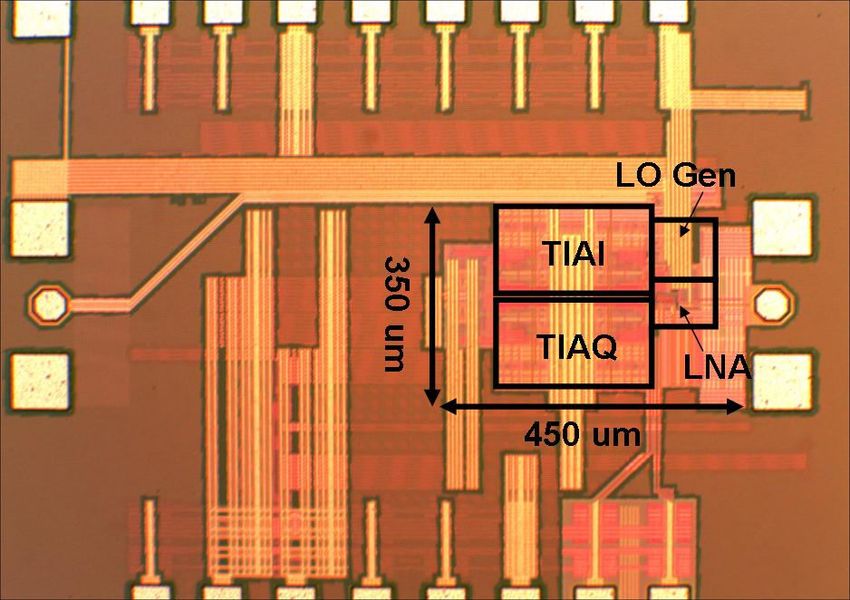
7.1 RF Front End Measurement Results
The RF front end prototype is fabricated in TSMC’s 45-nm CMOS technology
and characterized with a 1-V supply. Figure 7.1 displays the die photograph of
48the RF front end. The core area is around 0.16 mm2 . Tested at 2 GHz, this
prototype consumes 15 mW: 7 mW in the LNA, 5 mW in the TIAs, and 3 mW
in the 25%-duty-cycle LO generation circuit.
The measured NF is plotted in Fig.7.2. The LO frequency is at 2 GHz and
the baseband NF is measured across the entire bandwidth (0 35 MHz). The NF
ranges from 3.6 dB to 3.8 dB.
4
3.9
Noise figure (dB)
3.8
3.7
3.6
3.5
3.4
5 10 15 20 25 30
Frequency (MHz)
Figure 7.2: Measured noise figure.
Figure 7.3 shows the measured S11 of the front end. The LO frequency is at
2 GHz, and the S11 is below -10 dB across the entire LTE band.
The measured second and third intercept point are plotted in Fig. 7.4. The
LO frequency is at 1.96 GHz. In this two-tone test, the x-axis represents f1 while
f2 is placed at the frequency such that the intermodulation component stands at
3 MHz at the baseband output.
49−10.5
−11
−11.5
−12
S11 (dB)
−12.5
−13
−13.5
−14
−14.5
1960 1970 1980 1990 2000 2010 2020 2030 2040
Frequency (MHz)
Figure 7.3: Measured input matching.
50
40
30
IIP2
20
(dBm)
IIP3
10
0
−10
−20
1800 1850 1900 1950 2000 2050
Frequency (MHz)
Figure 7.4: Measured IIP2 and IIP3 .
507.2 Receiver Measurement Results
In this section, we test the entire receive chain, including the CMOS RF front end,
off-the-shelf ADCs and FPGA implementation. The RF signal is downconverted
to IF by the CMOS prototype and digitized by the ADCs. Since the interface
between ADCs and FPGA can not afford a speed faster than 50 MHz, the ADC
sampling rate is at 50 MS/s. The I and Q digital signals are reconstructed by
the proposed image-reject algorithm and downconverted to their baseband. We
test the receiver response to two carriers to demonstrate the achievable image-
rejection ratio across the entire band. As shown in Fig. 7.5, channel 2 is a
modulated strong signal while channel 1 is a single-tone weak signal.
Figure 7.5: Measured RF spectrum with two carriers.
Before digital I/Q reconstruction, Fig. 7.6 illustrates the image from channel
2 overwhelms channel 1 and the IRR is only 30 dB. After image-rejection recon-
struction, Fig. 7.7 demonstrates the image of channel 2 is below noise floor and
achieves an IRR greater than 70 dB. To demonstrate frequency-dependent I/Q
51compensation, Fig. 7.8 plots the IRR across the entire baseband.
Figure 7.6: Measured baseband spectrum with two carriers before image rejection.
52You can also read