Atomically-Precise Texturing of Hexagonal Boron Nitride Nanostripes
←
→
Page content transcription
If your browser does not render page correctly, please read the page content below
RESEARCH ARTICLE
 www.advancedscience.com

Atomically-Precise Texturing of Hexagonal Boron Nitride
Nanostripes
Khadiza Ali, Laura Fernández, Mohammad A. Kherelden, Anna A. Makarova, Igor Píš,
Federica Bondino, James Lawrence, Dimas G. de Oteyza, Dmitry Yu. Usachov,
Denis V. Vyalikh, F. Javier García de Abajo, Zakaria M. Abd El-Fattah, J. Enrique Ortega,*
and Frederik Schiller*

 1. Introduction
Monolayer hexagonal boron nitride (hBN) is attracting considerable attention
because of its potential applications in areas such as nano- and Hexagonal boron nitride (hBN) is an at-
 tractive two-dimensional (2D) material for
opto-electronics, quantum optics and nanomagnetism. However, the
 high performance electronics and photon-
implementation of such functional hBN demands precise lateral ics applications. It competes as insulat-
nanostructuration and integration with other two-dimensional materials, and ing substrate with SiO2 or Al2 O3 , and
hence, novel routes of synthesis beyond exfoliation. Here, a disruptive it is also promising as protective coating
approach is demonstrated, namely, imprinting the lateral pattern of an for metallic films that support intense 2D
atomically stepped one-dimensional template into a hBN monolayer. plasmons,[1,2] as a single photon emitter
 with deep UV lasing,[3] or as a supercon-
Specifically, hBN is epitaxially grown on vicinal Rhodium (Rh) surfaces using a
 ductor through suitable doping.[4] Although
Rh curved crystal for a systematic exploration, which produces a periodically hBN flakes may be obtained by mechan-
textured, nanostriped hBN carpet that coats Rh(111)-oriented terraces and ical exfoliation of bulk crystals, a single
lattice-matched Rh(337) facets with tunable width. The electronic structure hBN monolayer can be readily synthesized
reveals a nanoscale periodic modulation of the hBN atomic potential that on metal -surfaces,[5] leading to structurally
 and chemically robust substrates that fre-
leads to an effective lateral semiconductor multi-stripe. The potential of such
 quently exhibit nanoscale patterns. This
atomically thin hBN heterostructure for future applications is discussed. makes hBN-covered metals excellent plat-
 forms to achieve functional interfaces with
 atoms, molecules, and aggregates, as well as

Dr. K. Ali, Dr. L. Fernández, Prof. J. E. Ortega, Dr. F. Schiller Dr. I. Píš, Dr. F. Bondino
Centro de Física de Materiales CSIC/UPV-EHU-Materials Physics Center IOM-CNR
San Sebastián E-20018, Spain Laboratorio TASC
E-mail: enrique.ortega@ehu.es; frederikmichael.schiller@ehu.es Trieste I-34149, Italy
Dr. L. Fernández, Prof. J. E. Ortega Dr. I. Píš
Universidad del País Vasco Elettra - Sincrotrone Trieste S.C.p.A.
Dpto. Física Aplicada, San Sebastián E-20018, Spain Trieste I-34149, Italy
M. A. Kherelden, Dr. Z. M. A. El-Fattah Dr. J. Lawrence, Prof. D. G. de Oteyza, Prof. D. V. Vyalikh,
Physics Dept. Prof. J. E. Ortega, Dr. F. Schiller
Faculty of Science Donostia International Physics Center
Al-Azhar University San Sebastián E-20018, Spain
Nasr City, Cairo E-11884, Egypt Dr. D. Y. Usachov
Dr. A. A. Makarova St. Petersburg State University
Freie Universität Berlin St. Petersburg 199034, Russia
Berlin 14195, Germany Prof. D. V. Vyalikh
 Ikerbasque
 Basque Foundation for Science
 Basque Country, Bilbao 48013, Spain
 Prof. F. J. García de Abajo
 The ORCID identification number(s) for the author(s) of this article
 ICFO-Institut de Ciencies Fotoniques
 can be found under https://doi.org/10.1002/advs.202101455
 The Barcelona Institute of Science and Technology
© 2021 The Authors. Advanced Science published by Wiley-VCH GmbH. Barcelona 08860, Spain
This is an open access article under the terms of the Creative Commons Prof. F. J. García de Abajo
Attribution License, which permits use, distribution and reproduction in ICREA-Institució Catalana de Recerca i Estudis Avançats
any medium, provided the original work is properly cited. Passeig Lluís Companys 23, Barcelona 08010, Spain
DOI: 10.1002/advs.202101455

Adv. Sci. 2021, 8, 2101455 2101455 (1 of 9) © 2021 The Authors. Advanced Science published by Wiley-VCH GmbH
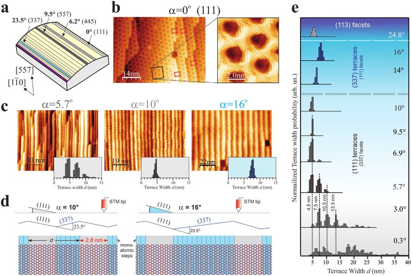
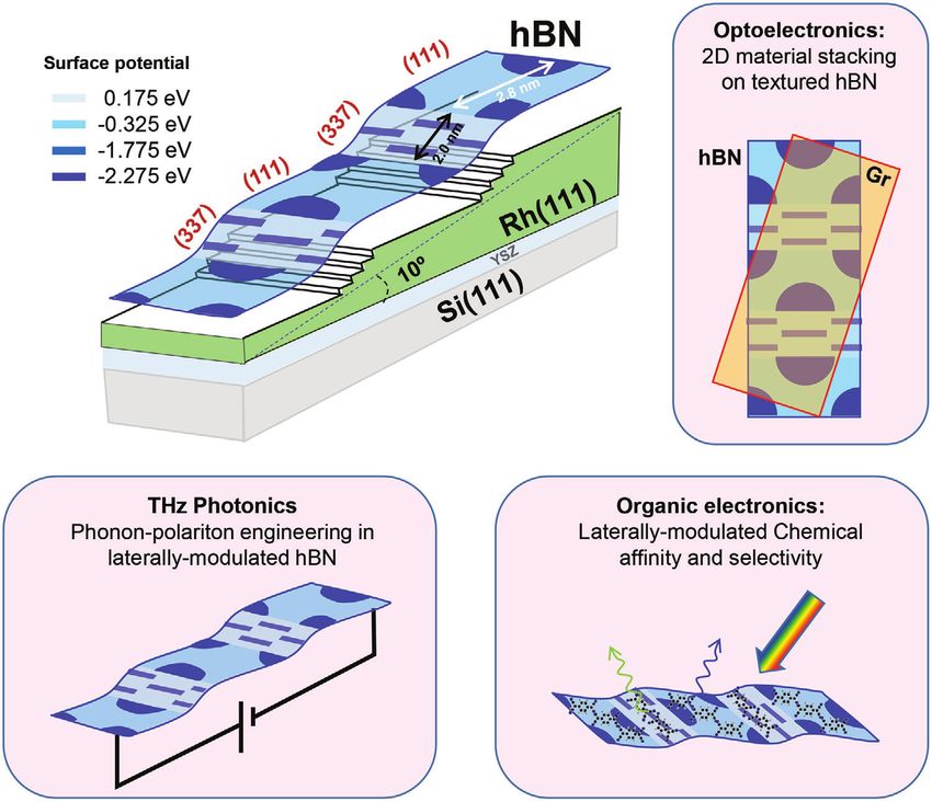
www.advancedsciencenews.com www.advancedscience.com

Figure 1. Lateral nanopatterning of hBN through epitaxial growth. We explore this concept by studying vicinal hBN/Rh interfaces. CVD growth of
hBN induces periodic (111)/(337) faceting of the Rh substrate. The hBN monolayer uniformly coats the faceted substrate, defining an effective lateral
hBN/hBN heterointerface with periodic surface potential texturing. Using commercial Rh(111) films[17,18] one could exploit such chemical and electronic
modulation of hBN to explore phonon–polariton THz excitations, selective growth of optically-active molecules, and vertical stacking with other 2D
materials.

to develop hybrid 2D materials, such as twisted van der Waals tem as a model platform to mold and probe 1D phonon–polariton
stacks or 2D heterostructures.[6–8] The latter hold a great poten- excitations in the THz regime,[15] to achieve selective growth of
tial for atomically thin circuitry, such as superstructures formed atoms, aggregates, and molecular adsorbates for organic opto-
with isostructural graphene,[9–13] which are optimal to engineer electronics and catalysis,[5,16] and to tailor the 3D stacking with
gaps and doping, as well as to tune and enhance spin scatter- other 2D materials, such as graphene.[7]
ing. However, exploiting fine hBN-based nanostructures requires
structural quality down to the atomic scale, which lies beyond
current lithographic capabilities. The bottom-up vapor growth is 2. hBN-Induced Faceting across a Rh Curved
the alternative, which also works for 2D hybrids,[14] although gen- Surface
eral procedures to control shape, size, and spatial order of surface
phases are still lacking. We examined striped hBN monolayers over an ample range of
 Here, we demonstrate the bottom-up synthesis of nanostriped Rh vicinal orientations with a curved Rh surface (c-Rh). The sam-
hBN heterostructures with atomically sharp interfaces. We follow ple is schematically depicted in Figure 2a. It is a cylindrical sec-
the standard chemical vapor deposition (CVD) growth route, us- tion of a Rh single crystal with the cylinder axis along [110] direc-
ing Rhodium (Rh) vicinal surfaces as one-dimensional (1D) tem- tion. The curved surface spans all vicinal surfaces ( angle) from
plates. We show that the excellent registry with the Rh(337) plane the high symmetry (111) ( = 0) at the right edge of the sample,
triggers periodic (111)/(337) faceting of the substrate, as sketched passing through the (557) plane ( = 9.5°) at the sample center,
in Figure 1. The hBN monolayer carpet-coats the faceted sub- and reaching the (337) surface ( = 23.5°) near the left side edge.
strate, but the distinct symmetry and atomic interaction at each The freshly prepared surface is heated to T = 1000K, and then
hBN/Rh phase give rise to a textured and periodically modulated exposed to borazine, leading to full monolayer coverage of hBN
surface potential. A 1D lateral hBN (111)/(337) heterostructure across the entire curve, as judged from scanning tunneling mi-
arises, featuring defect-free boundaries and significant band off- croscopy (STM) and low energy electron diffraction (LEED). At
sets. Since size tunability of phases can be gained by selecting the Rh(111) plane, this results in a hBN nanomesh structure,[19]
the Rh vicinal plane, we envision the hBN (111)/(337) faceted sys- which arises due to atomic lattice mismatch and variable bonding

Adv. Sci. 2021, 8, 2101455 2101455 (2 of 9) © 2021 The Authors. Advanced Science published by Wiley-VCH GmbH
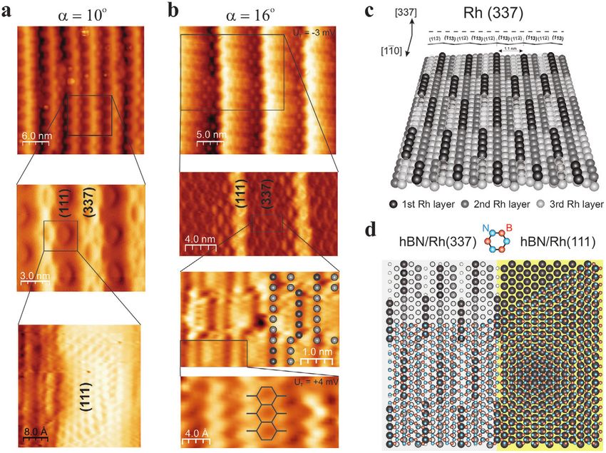
www.advancedsciencenews.com www.advancedscience.com

Figure 2. Evolution of the hBN nanostriped system on a curved Rh surface. a) Sketch of the c-Rh sample with some vicinal angles and corresponding
crystal planes indicated. b) 4K-STM image and zoom-in near the hBN-covered Rh(111) plane ( = 0). c) 300K-STM topographies and terrace width
histograms at characteristic angles: (111) terraces reveal discretized hBN nanomesh quanta ( = 5.7°), a single nanomesh quantum ( = 10°), and
hBN-(337) nanostripes ( = 16.0°). d) Description of the STM scan over the hBN/Rh interface at = 10° and = 16°, where hBN-(111) and hBN-(337)
nanostripes are respectively imaged as “terraces.” e) Terrace width distribution histograms across the curved hBN/c-Rh surface. At low (gray region),
peaks correspond to multiples of the (111) nanomesh, down to a single quantum at = 10°. Above = 10° (blue region), the distribution shifts to the
right side, reflecting the increasing width of the (337) facets. Beyond the (337) plane ( > 23.5°, purple region), (113) faceting arises.

between the hBN layer and the Rh substrate.[20] Images in Figure mation). The histogram points to an interface that is broken up
2b, acquired with a 4K-STM, show the atomically resolved struc- in a random distribution of hBN-covered (111) terraces of width
ture close to the Rh(111) plane and near substrate steps. We ob- d ≈ 4.6, 7.1, and 9.6 nm, alternated with step bunches. Conse-
serve that (111) terraces are delimited by steps corresponding to quently, the terrace width increases approximately in multiples
Rh(111) single step height, with upper and lower terraces coated of the nanomesh periodicity in the perpendicular direction to the
with a continuous hBN film. Within (111) terraces, the lattice con- steps (nanomesh quantum Δd ≈ l × cos 30° = 2.8 nm). The lowest
stant of the hexagonal nanomesh is l = 3.2 nm, agreeing with value d ≈ 4.6 nm agrees with the nanomesh quantum plus the ef-
former studies,[19,20] while across the steps the pore lattice is co- fective width of the step bunch (1.8 nm). The central panel of Fig-
herently connected (red rectangles), indicating that hBN forms a ure 2c corresponds to the surface at = 10°. At this vicinal angle,
continuous layer that carpets atomic steps (see also Supporting the hBN monolayer becomes a periodic structure with d ≈ 5 nm
Information for a graphical demonstration). of nanostripes delimited by bunches of 3–5 monatomic steps
 Away from the (111) direction, the hBN monolayer interacts and, most important, with minimal size fluctuations around one
with the step array of the substrate elastically, leading to faceting. nanomesh quantum.
We examined such interaction across the entire hBN-covered c- The right-hand side STM micrograph of Figure 2c displays
Rh surface by STM at T = 300 K. Figure 2c shows STM images the growth of hBN on a densely stepped c-Rh area at = 16°.
acquired at three characteristic points at = 5.7°, 10°, and 16°, In the STM image we observe well-defined hBN nanostripes, but
together with their respective terrace-width d distribution his- compared with the = 10° image, terraces appear wider with d ≈
tograms. At = 5.7° we observe straight and parallel hBN nanos- 8 nm and the step direction has reversed from uphill to down-
tripes, which fit in Rh(111) terraces of discrete sizes, separated hill. This effect is schematically explained in Figure 2d. At
by bunches of one to four Rh atomic steps (see Supporting Infor- = 10°, (111)-oriented nanostripes are wider than hBN-covered

Adv. Sci. 2021, 8, 2101455 2101455 (3 of 9) © 2021 The Authors. Advanced Science published by Wiley-VCH GmbH
www.advancedsciencenews.com www.advancedscience.com

Figure 3. Atomic structure of hBN-covered Rh(111)-(337) facets. a) and b) 4K-STM topographies (top) and progressive filtered zoom-ins (second to
bottom) at = 10° and = 16°, respectively. b) The atomic positions of the step in the reconstructed (337) surface appear overlaid (third image), as well
as the hBN lattice (fourth image). c) Model for the Rh(337) surface with selective step atom removal (white dashed balls). Black balls mark the outermost
surface atoms, while gray balls become lighter in successive surface levels. d) Model for a continuous hBN monolayer (blue-red balls and sticks) in a
coherent (111)/(337) lateral interface. In hBN/Rh(111), the coincidence lattice leads to nanomesh pores around N/Rh on-top sites. In hBN/Rh(337),
black balls mark the out-protruding step atoms, which correspond to N/Rh on-top sites of the hBN overlayer.

step bunches, and hence (111) nanostripes appear as terraces in investigated in detail using 4K-STM. Images in Figure 3a,b have
the STM image. At = 16° (111) nanostripes are narrower than been acquired again at = 10° and = 16° on the c-Rh surface.
stepped facets, which are thus imaged as terraces, while hBN- The larger view in top panels corresponds to the direct topogra-
(111) nanostripes appear as downhill steps. 4K-STM, ARPES, and phy, while lower panels are image derivatives showing progres-
LEED experiments (see below) prove that the orientation of the sive zoom-ins acquired at varied tip bias. Such image processing
stepped facets is the Rh(337) direction. This transition in the ori- removes the hill-and-valley modulation, allowing us to define the
entation of the apparent terrace beyond = 10° is reflected in the lateral (111)/(337) interface, which shows no sign of discontinu-
terrace-width distribution analysis performed across the entire ity. From 10° to 16°, (337) terraces widen from d337 = 2 nm to
surface, shown in Figure 2e. This provides an unified picture ≈8 nm, while the (111) nanostripe width barely changes. The in-
of the hBN/c-Rh interface. In the < 10° range, (111)-oriented ternal structure of each phase is visualized in the bottom panels
terraces are discrete multiples of the perpendicular nanomesh. of Figure 3a,b. This includes the hBN atomic lattice in both hBN-
With increasing , the center of gravity of the terrace width dis- (111) and hBN-(337) nanostripes, as indicated with the overlaid
tribution shifts toward the first nanomesh quantum. For > 10°, structure. The hBN-(111) nanostripe shows a wavy wire running
hBN-(337) nanostripes turn into apparent terraces, and hence, parallel to the step [bright protrusion in top panel of (b)], with
the histogram shifts to the right side reflecting the increasing half-pores at nanostripe boundaries. The hBN-(337) nanostripe
(337) terrace width. Importantly, a sharp size distribution re- exhibits a characteristic texture, with the l = 3.2 nm nanomesh
mains, demonstrating that hBN-(337) nanostripes have a single periodicity in the parallel direction, and a reduced one of 1.1 nm
characteristic width at each vicinal angle over the 10° < < 23.5° perpendicular to the steps, both defining a 2D structure with uni-
range. Beyond 23.5°, hBN-(111) nanostripes disappear and hBN- axial symmetry. Such nanoscale texture in the hBN layer is ex-
covered (113) facets emerge. plained by the periodic re-arrangement of the Rh(337) substrate
 steps described in Figure 3c.
3. The hBN-Covered Rh(111)/Rh(337) Interface Adsorption-induced faceting of vicinal surfaces is driven by the
 optimal registry of the adlayer atomic lattice with the step spac-
Next we focus on the hBN-induced Rh(111)-Rh(337) periodic ing, such as to reduce interface strain.[21] For hBN/metal systems,
faceting, which exhibits straight, and sharply defined hBN nanos- characteristic facets are expected for step periodicities that match
tripes with coherent coupling between (111) and (337) phases. an entire number of hBN cells.[22] In the hBN/Rh system, we may
The atomic arrangement at the hBN/Rh interface of each phase is compare the step spacing in the Rh(337) plane with the distance

Adv. Sci. 2021, 8, 2101455 2101455 (4 of 9) © 2021 The Authors. Advanced Science published by Wiley-VCH GmbH
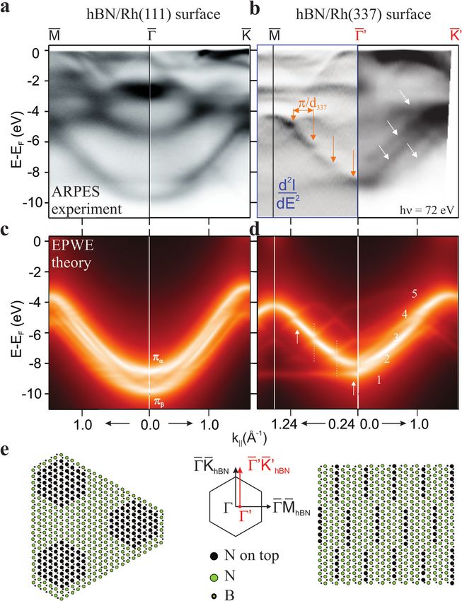
www.advancedsciencenews.com www.advancedscience.com

between contiguous N rows in hBN. As shown in Figure 3c, the Table 1. band properties in hBN/metal systems. band bottom (Γ̄ min ),
(337) plane can be viewed as an alternating sequence of (112) and top (K̄ max ), and bandwidth (ΔΓM ) measured with ARPES in hBN/metal
 systems. Data for hBN/Ni(111) and hBN/Au/Ni(111) are from Ref. [24].
(113) terraces, resulting in a l337 = 1.1 nm lattice constant perpen-
 ⟨VN ⟩w, p and m* respectively are the average surface potential at N atoms
dicular to the steps. This closely corresponds to five rows of N for wires and pores, and the effective mass used in the EPWE model, which
atoms (5 × ahBN × cos 30° = 1.08 nm) in the hBN monolayer with renders the semiconducting gap (EF gap). All magnitudes are expressed
ahBN = 2.504Å being the hBN lattice constant. Thus, by slightly in eV.
(2%) stretching the hBN monolayer, only N atom rows are in co-
incidence with the out-protruding step-edge. Yet, the mismatch Interface Γ̄ min K̄ max ΔΓM EF gap w p
along the steps leads to periodic off-registry (strained) N-bridge
 hBN/Au/Ni(111) −8.2 −2.22 4.87 5.08 0.0 0.0 1.00
positions. The substrate reconstruction proposed in Figure 3c
 hBN/Ni(111) −10.0 −4.45 4.53 5.08 −1.690 −1.690 1.05
solves this problem.
 hBN/Rh(111) −9.8 ±0.2 −3.0 ±0.2 4.4 ±0.1 4.20 −0.325 −2.275 1.03
 The Rh(337) unit cell contains two rows of step atoms at differ-
ent levels, with the outermost one corresponding to the downhill hBN/Rh(337) −8.8 ±0.2 −3.3 ±0.2 2.86 ±0.1 4.87 0.175 −1.775 1.10

step of the (112) terrace. As shown in Figure 3c, removal of 7 out
of 12 step atoms in this row (dashed-white transparent balls) re-
verses the (112)–(113) series and moves the contiguous step seg- only four parameters, namely, the different scattering potentials
ments at the topmost surface position. Now, the outermost sur- at N and B atoms, a rigid potential shift ΔV from wires to pores
face layer (black balls) is made of 5–6 step-atom segments, defin- (first Fourier component of the nanoscale potential), and an ef-
ing a 2D lattice identical to that imaged in Figure 3b. In Figure 3d fective mass m*, we fit the experimentally observed energies at
we overlay the hBN lattice on top of a (111)/(337) interface. The ̄ M,
 Γ, ̄ and K̄ points, and obtain the theoretical bands of Figure 4c
Rh(337) step re-arrangement has the double effect of eliminating (see also Figure S4, Supporting Information for more details). We
7 off-registry N-bridge step sites, while creating six new registry N indeed find that a band splitting arises for ΔV < 0. To fit ARPES
on-top step sites. Thus, the Rh(337) reconstruction relieves strain bands we require ΔV = −1.95 eV and m* = 1.03· me , with me be-
by improving registry, making the hBN/Rh interface more robust ing the free electron mass (see Table 1). Actually, due to the (13 ×
through exclusive N/Rh on-top bonding. Note that the l = 3.2 nm 13) periodicity, the simple EPWE model delivers multiple band
nanomesh periodicity remains along the steps, enabling the co- replicas within the hBN Brillouin zone, which are averaged out by
herent coupling with neighboring hBN-(111) nanostripes, which introducing broadening in the photoemission probability. Note
in turn explains the smooth coating of the faceted substrate (see that experimental bands in Figure 4a only mirror the hexagonal
also Figure S8, Supporting Information for a graphical explana- symmetry of the atomic lattice, but do not show nanomesh umk-
tion). Similar hBN/Rh step-lattice registry and density of N on-top lapps, sometimes seen for graphene/metal moiré systems.[27,28]
step anchoring points can be obtained when considering separate In the hBN/Rh(337) bands, the uniaxial symmetry brought in
hBN/Rh(112) and hBN/Rh(113) interfaces, as shown in Figure by the nanoscale texture is reflected in the band structure, shown
S3, Supporting Information. However, in (112) and (113) planes, in Figure 4b. Data correspond to = 24°, that is, very close to the
off-registry N bridge-bonding to step atoms remains, in contrast Rh(337) surface. Due to experimental restrictions we were not
to the sole N on-top bonding of Figure 3c, which only the Rh(337) able to measure in the exact Γ̄ K̄ hBN direction but only close to it as
plane allows. indicated in the middle panel of Figure 4e. Nevertheless, we now
 observe a striking asymmetry from the perpendicular (Γ̄ M ̄ hBN ) to
 ̄ ′̄′
4. Uniaxial Band Symmetry in the hBN-(337) the parallel (Γ KhBN ) direction along substrate steps. Perpendicu-
Surface lar to the steps, the main dispersing feature is broken up in seg-
 ments, separated by ≈0.3 meV mini-gaps (see arrows; the second
The structurally different hBN/Rh(111) and hBN/Rh(337) phases derivative of the image enhances gap visualization, see Support-
exhibit distinct electronic bands, which we display in Fig- ing Information), whereas in the parallel direction the band
ures 4a,b. The (111)-nanomesh modulation triggers the split- splits in a set of continuous sub-bands (inclined arrows). Such
ting of all hBN electron levels,[19,23] from vacuum to valence distinct band topology is correctly reproduced in EPWE calcula-
and core bands, in contrast to the simple sequence of electronic tions of Figure 4d, which are based on the atomic model depicted
states in non-interacting or registry hBN monolayers.[24] Figure in Figure 4e. Note that despite the apparent atomic complexity,
4a shows the electron bands measured with ARPES along the the hBN/Rh(337) interface is simple in terms of bonding, since
 ̄ hBN and Γ̄ K̄ hBN directions in the hBN/Rh(111) system ( =
Γ̄ M all the outermost Rh step atoms bind to N in atop positions. For
0). The Rh substrate emission dominates the spectrum from the EPWE model, it is thus reasonable to assume the same sur-
the Fermi energy down to −3 eV, while and bands of hBN face potential reduction at N atoms on steps that was used for
appear below this energy. The characteristic – splitting is pores, ΔV = −1.95 eV. In excellent correspondence with the ex-
observed,[23] due to the different interaction with the Rh substrate perimental observations in Figure 4b, the model reveals the pres-
at pores and wires.[25] As explained from density-functional- ence of a fivefold band splitting at Γ, ̄ which leads to a set of
theory (DFT),[23,25] the highly bound band originates in the dispersing bands along Γ̄ K̄ hBN , and to five mini-bands separated
highly interacting on-top N atoms in the pores, while the by mini-gaps at Rh(337) Brillouin zone edges (n × /d337 ) along
branch comes from off-registry N atoms in the wires. ̄ hBN .
 Γ̄ M
 The pore/wire nature of the / split-bands in the The hBN/Rh(337) system represents the first successful case
hBN/Rh(111) interface is well captured in our electron-plane- of uniaxial symmetry imprinted onto the electronic structure of
wave-expansion (EPWE) and photoemission model.[26] Using the hBN monolayer. In pursue of this objective, (110)-oriented

Adv. Sci. 2021, 8, 2101455 2101455 (5 of 9) © 2021 The Authors. Advanced Science published by Wiley-VCH GmbH
www.advancedsciencenews.com www.advancedscience.com

Figure 4. hBN electron bands on Rh(111) and Rh(337). a,b) Experimental hBN bands along the Γ̄ M, ̄ Γ̄ K,
 ̄ and Γ̄ ′ K̄ ′ directions measured with ARPES
in the Brillouin zones of hBN/Rh(111) and hBN/Rh(337) as indicated in (e). For hBN/Rh(337) in (b), arrows mark mini-gaps at n × /d337 Brillouin
 ̄ and the band manifold along Γ̄ ′ K̄ ′ . c,d) Theoretical hBN bands calculated with the EPWE model, assuming the different atomic
zone edges along Γ̄ M
potentials at pores/steps (N black) and wires (N green) shown in (e). The fivefold band splitting along Γ̄ ′ K̄ ′ is numbered from bottom to top in (d).

metal surfaces were tested in the past,[29–32] but the hBN film exception,[22] and this can serve to pinpoint new “magic,” well-
was observed to break up in rotational phases. On Rh(110),[33] matched surfaces, such as Rh(337), and to find nanostriped pat-
hBN nanostriped domains appear, reflecting the scarcity of fa- terns with varied textures.
vorable interface (N on-top) bonding sites compared to recon- In Table 1 we summarize the band properties for fundamen-
structed Rh(337). Nevertheless, away from high symmetry direc- tal hBN/Rh systems, namely, free-standing (Au/Ni), 2D atomic-
tions, other hBN/metal surface combinations should exist with registry [Ni(111)], 2D nanomesh [Rh(111)], and 1D step-registry
optimal lattice matching. Uniaxial vicinal planes with different [Rh(337)], from which we derive some trends. The band mini-
terrace orientations, such as (110), (110), or (201), as well as mum at Γ̄ (Γ̄ min ) is connected to the ratio of substrate-interacting
other metals, such as Pt, Pd, Ru, or Cu should be explored.[5] N atoms in top positions to the total number of N atoms. Such
hBN-induced faceting appears to be the rule rather than the ratio increases from 20% in Rh(337) steps, to 40% in Rh(111)

Adv. Sci. 2021, 8, 2101455 2101455 (6 of 9) © 2021 The Authors. Advanced Science published by Wiley-VCH GmbH
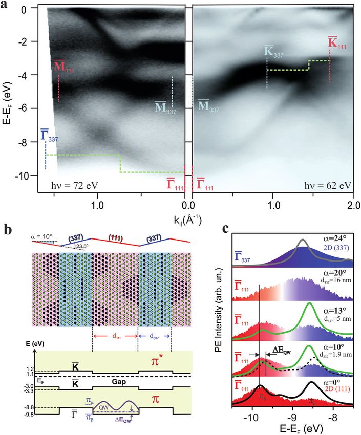
www.advancedsciencenews.com www.advancedscience.com

Figure 5. Electronic states in lateral hBN heterostructures. a) Electron bands for the hBN (111)/(337) superlattice measured with ARPES (h = 72 eV)
at = 10° in the hBN/c-Rh sample. The faceted geometry leads to separate emission from (111) and (337) facets. The respective Γ, ̄ K̄ symmetry
 ̄ M,
points and the resulting heterostructure offsets are indicated. b) Atomic model and band diagram for the hBN (111)/(337) lateral heterostructure, as
determined from data and calculations of Figure 4. c) Evolution of the ARPES intensity at Γ̄ 111 in the (111)/337 nanostriped system at increasing . The
spectrum on top corresponds to the Γ̄ 337 point of the 2D hBN-(337) system. Lines are EPWE spectra at Γ̄ for heterostructures of fixed d111 = 2.8 nm
and variable d337 . ΔEQW marks the expected EPWE shift of in fully decoupled 2.8 nm d111 nanostripes.

pores, and to 100% in lattice-matched Ni(111), and directly cor- heterostructure. In Figure 5a we show electron bands as obtained
relates with the average ⟨VN ⟩ potential in the EPWE model. De- from ARPES measurements at = 10° along Γ̄ M ̄ hBN and Γ̄ K̄ hBN ,
spite the strong difference in interface bonding, the hBN gap re- where the superlattice is formed by d111 = 2.8 nm and d337 ≈2 nm
mains unchanged in Ni and Au/Ni, whereas nanoscale texturing hBN nanostripes. This nanostriped system is depicted in Figure
in Rh(111) and Rh(337) effectively reduces the gap. 5b, together with its band diagram, where we have assumed the
 energies of Table 1 to define valence and conduction band offsets.
5. Electronic States in Lateral hBN (111)/(337) Interestingly, the hill-and-valley geometry of the surface plane
Heterostructures leads to separate intensity from (111)- and (337)-oriented facets
 in ARPES scans (see Figure S6, Supporting Information for de-
The straight boundaries with coherent atomic bonding, together tails). This allows us to track the evolution of the band emis-
with the distinct band properties of (111)- and (337)-oriented hBN sion from each phase, and hence to prove (111)/(337) electronic
nanostripes define an ideal atom-thick, lateral semiconductor coupling. This is done for the 2.8-nm-wide d111 nanostripe in

Adv. Sci. 2021, 8, 2101455 2101455 (7 of 9) © 2021 The Authors. Advanced Science published by Wiley-VCH GmbH
www.advancedsciencenews.com www.advancedscience.com

Figure 5c. Red-blue shaded spectra correspond to k|| = 0 in the adding an appealing alternative to the suite of existing possibili-
(111) plane (Γ̄ 111 point), whereas green curves are EPWE calcula- ties in the THz region.
tions for the heterostructure of Figure 5b, assuming d337 nanos-
tripes of increasing width. The spectral density clearly evolves
from the hBN-(111) system (bottom) to hBN-(337) (top) as a func- Supporting Information
tion of , that is, from the 2D (111) nanomesh to increasingly
sparse d111 = 2.8 nm nanostripes. Because of the 1 eV valence Supporting Information is available from the Wiley Online Library or from
band offset at the interface, the peak, which lies below the the author.
band minimum in the (337) plane (Γ337 ), is weakly coupled to
the (337) bands. Consequently, behaves as a (111)-terrace-like
state, which shifts up in energy and has its intensity reduced Acknowledgements
when the (111) surface evolves into a narrow stripe. In contrast,
 The authors acknowledge financial support from the Spanish Ministry of
the feature that lies above the Γ337 minimum resonates with
 Science and Innovation (Grants MAT-2017-88374-P, PID2019-107338RB-
the (337) band and hence remains intense. Note that we are exclu- C63, MAT2017-88492-R, and Severo Ochoa CEX2019-000910-S), the CSIC
sively probing emission from d111 -oriented areas of the surface. (Grant 2020AEP178), the Basque Government (Grant IT-1255-19), the
Thus, Figure 5c demonstrates that d111 nanostripes embedded Marie Sklodowska-Curie European Union’s Horizon 2020 program (grant
within large d337 areas at = 20° produces emission that is co- MagicFACE 797109), the European Research Council (Advanced Grant
herent with the hBN-(337) system. In fact, the asymmetric inten- 789104-eNANO), and Elettra Sincrotrone Trieste for providing access to
sity variation of and , as well as the small (50 meV) shift of its synchrotron radiation facilities. I.P. and F.B. acknowledge funding from
 EUROFEL, and D.U. from the Ministry of Science and Higher Education
 , are reproduced in our calculations for electronically-coupled
 of the Russian Federation [Grant No. 075-15-2020-797 (13.1902.21.0024)].
111/337 interfaces. In contrast, our calculations permit us to dis- A.A.M. acknowledges the German Ministry for Education and Research
card a fully decoupled, quantum-well-like d111 nanostripe (black (Grant 05K19KER). The article was amended on July 30, 2021 to correct
dotted spectrum in Figure 5c), which would produce spectra ex- the name of Federica Bondino.
hibiting a symmetric – intensity quenching, and a substan-
tially larger peak shift (ΔEQW = 150 meV).
 Conflict of Interest
6. Conclusions
 The authors declare no conflict of interest.
We have explored a novel approach to nanopatterning a material
with practical technological impact, namely growing hBN mono-
layers on vicinal surfaces. Growth of hBN on vicinal Rh(111)
 Data Availability Statement
leads to periodic (111)/(337) faceting, triggered by excellent
atomic registry of hBN with a step-reconstructed (337) surface Research data are not shared.
plane. The hBN film forms a continuous layer over the faceted
system with alternated (111) and (337) phases, each exhibiting
a characteristic internal texturing, and strain-free atomic bond-
 Keywords
ing at the mutual interface, thereby defining an electronically-
coherent hBN lateral heterostructure. boron nitride nanostripes, photoemission, scanning tunneling mi-
 In the context of the rich phenomenology exhibited in croscopy, uniaxial electronic bands
hBN/metal interfaces,[5] we devise a vast number of possibili-
ties for vicinal surfaces. These are known to drive the nucleation Received: April 9, 2021
 Revised: May 25, 2021
and growth of azimuthally-oriented hBN flakes,[34,35] and here
 Published online: July 22, 2021
we show that they also trigger 1D texturing, as depicted in Fig-
ure 1. Beyond the (111)/(337) system, other hBN/metal orien-
tations may also exhibit faceting with distinct electronic proper-
ties and textures, and this could be systematically explored with [1] I. Lončarić, Z. Rukelj, V. M. Silkin, V. Despoja, npj 2D Mater. Appl.
curved surfaces. The nanoscale corrugation of the surface poten- 2018, 2, 33.
tial can help to imprint, for example, a periodic modulation of [2] K. Watanabe, T. Taniguchi, T. Niiyama, K. Miya, M. Taniguchi, Nat.
energy and filling of molecular levels in organic adsorbates.[16] Photonics 2009, 3, 591.
It can also have a strong influence in epitaxial growth, for exam- [3] J. D. Caldwell, I. Aharonovich, G. Cassabois, J. H. Edgar, B. Gil, D.
ple, in the vertical stacking of transition metal dichalcogenides Basov, Nature 2019, 41578, 019.
(TMDs) or graphene, where it may help to tune, in general, elec- [4] N. H. Shimada, E. Minamitani, S. Watanabe, Appl. Phys. Express 2017,
 10, 093101.
tronic properties[36] and, in particular, the twist angle.[7] The po-
 [5] W. Auwärter, Surf. Sci. Rep. 2019, 74, 1.
tential for optoelectronics of such 2D material stacking should
 [6] F. Withers, O. DelPozo-Zamudio, A. Mishchenko, A. P. Rooney, A.
also be explored for applications, such as band structure modula- Gholinia, K. Watanabe, T. Taniguchi, S. J. Haigh, A. K. Geim, A. I. Tar-
tion of graphene and TMDs. The hBN (111)/(337) heterostruc- takovskii, K. S. Novoselov, Nat. Mater. 2015, 14, 301.
ture is also an ideal platform to manipulate phonon-polariton [7] R. Ribeiro-Palau, C. Zhang, K. Watanabe, T. Taniguchi, J. Hone, C. R.
excitations and their dynamics.[15] The band structure modula- Dean, Science 2018, 361, 690.
tion is expected to affect the optical response of the material, thus [8] M. Kan, Y. Li, Q. Sun, WIREs Comput. Mol. Sci. 2016, 6, 65.

Adv. Sci. 2021, 8, 2101455 2101455 (8 of 9) © 2021 The Authors. Advanced Science published by Wiley-VCH GmbH
www.advancedsciencenews.com www.advancedscience.com

 [9] L. Ci, L. Song, C. Jin, D. Jariwala, D. Wu, Y. Li, A. Srivastava, Z. F. Wang, [23] T. Brugger, S. Günther, B. Wang, J. H. Dil, M.-L. Bocquet, J. Oster-
 K. Storr, L. Balicas, F. Liu, P. M. Ajayan, Nat. Mater. 2010, 9, 430. walder, J. Wintterlin, T. Greber, Phys. Rev. B 2009, 79, 045407.
[10] M. P. Levendorf, C.-J. Kim, L. Brown, P. Y. Huang, R. W. Havener, D. [24] D. Usachov, V. K. Adamchuk, D. Haberer, A. Grüneis, H. Sachdev, A.
 A. Muller, J. Park, Nature 2012, 488, 627. B. Preobrajenski, C. Laubschat, D. V. Vyalikh, Phys. Rev. B 2010, 82,
[11] L. Liu, J. Park, D. A. Siegel, K. F. McCarty, K. W. Clark, W. Deng, L. 075415.
 Basile, J. C. Idrobo, A.-P. Li, G. Gu, Science 2014, 343, 163. [25] R. Laskowski, P. Blaha, T. Gallauner, K. Schwarz, Phys. Rev. Lett. 2007,
[12] C. Leon, M. Costa, L. Chico, A. Latgé, Sci. Rep. 2019, 9, 3508. 98, 106802.
[13] H. S. Wang, L. Chen, K. Elibol, L. He, H. Wang, C. Chen, C. Jiang, [26] Z. M. Abd El-Fattah, M. A. Kher-Elden, I. Piquero-Zulaica, F. J. G. de
 C. Li, T. Wu, C. X. Cong, T. J. Pennycook, G. Argentero, D. Zhang, Abajo, J. E. Ortega, Phys. Rev. B 2019, 99, 115443.
 K. Watanabe, T. Taniguchi, W. Wei, Q. Yuan, J. C. Meyer, X. Xie, Nat. [27] E. Starodub, A. Bostwick, L. Moreschini, S. Nie, F. E. Gabaly, K. F.
 Mater. 2021, 20, 202. McCarty, E. Rotenberg, Phys. Rev. B 2011, 83, 125428.
[14] P. Sutter, Y. Huang, E. Sutter, Nano Lett. 2014, 14, 4846. [28] E. Rotenberg, A. Bostwick, Synth. Metals 2015, 210, 85.
[15] H. Chen, H. Liu, Z. Zhang, K. Hu, X. Fang, Adv. Mater. 2016, 28, 403. [29] M. P. Allan, S. Berner, M. Corso, T. Greber, J. Osterwalder, Nanoscale
[16] F. Schulz, R. Drost, S. K. Hämäläinen, P. Liljeroth, ACS Nano 2013, 7, Res. Lett. 2007, 2, 94.
 11121. [30] N. A. Vinogradov, A. A. Zakharov, M. L. Ng, A. Mikkelsen, E. Lund-
[17] S. Gsell, M. Fischer, M. Schreck, B. Stritzker, J. Cryst. Growth 2009, gren, N. Mårtensson, A. B. Preobrajenski, Langmuir 2012, 28, 1775.
 311, 3731. [31] T. Greber, L. Brandenberger, M. Corso, A. Tamai, J. Osterwalder, J.
[18] A. Hemmi, C. Bernard, H. Cun, S. Roth, M. Klöckner, T. Kälin, M. Surf. Sci. Nanotechnol. 2006, 4, 410.
 Weinl, S. Gsell, M. Schreck, J. Osterwalder, T. Greber, Rev. Sci. Instrum. [32] M. Corso, T. Greber, J. Osterwalder, Surf. Sci. 2005, 577, L78.
 2014, 85, 035101. [33] A. J. Martínez-Galera, J. M. Gómez-Rodríguez, Nano Res. 2018, 11,
[19] M. Corso, W. Auwärter, M. Muntwiler, A. Tamai, T. Greber, J. Oster- 4643.
 walder, Science 2004, 303, 217. [34] L. Wang, X. Xu, L. Zhang, R. Qiao, M. Wu, Z. Wang, S. Zhang, J. Liang,
[20] A. B. Preobrajenski, A. S. Vinogradov, N. Mårtensson, Phys. Rev. B Z. Zhang, Z. Zhang, W. Chen, X. Xie, J. Zong, Y. Shan, Y. Guo, M.
 2004, 70, 165404. Willinger, H. Wu, Q. Li, W. Wang, P. Gao, S. Wu, Y. Zhang, Y. Jiang, D.
[21] A. Bachmann, S. Speller, A. Mugarza, J. Ortega, Surf. Sci. 2003, 526, Yu, E. Wang, X. Bai, Z.-J. Wang, F. Ding, K. Liu, Nature 2019, 570, 91.
 L143. [35] L. Zhang, P. Peng, F. Ding, Adv. Funct. Mater. 2021, 31, 2100503.
[22] L. Fernandez, A. A. Makarova, C. Laubschat, D. V. Vyalikh, D. Y. Usa- [36] Q. Zhang, Y. Chen, C. Zhang, C.-R. Pan, M.-Y. Chou, C. Zeng, C.-K.
 chov, J. E. Ortega, F. Schiller, 2D Mater. 2019, 6, 025013. Shih, Nat. Commun. 2016, 7, 13843.

Adv. Sci. 2021, 8, 2101455 2101455 (9 of 9) © 2021 The Authors. Advanced Science published by Wiley-VCH GmbH
You can also read