Boolean Algebra and Digital Logic
←
→
Page content transcription
If your browser does not render page correctly, please read the page content below
CHAPTER 3
                  Boolean Algebra and Digital Logic
3.1 Introduction 135
3.2 Boolean Algebra 136
      3.2.1 Boolean Expressions 137
      3.2.2 Boolean Identities 138
      3.2.3 Simplification of Boolean Expressions 140
      3.2.4 Complements 143
      3.2.5 Representing Boolean Functions 144
3.3 Logic Gates 146
      3.3.1 Symbols for Logic Gates 146
      3.3.2 Universal Gates 147
      3.3.3 Multiple Input Gates 148
3.4 Karnaugh Maps 149
      3.4.1 Introduction 149
      3.4.2 Description of Kmaps and Terminology 149
      3.4.3 Kmap Simplification for Two Variables 151
      3.4.4 Kmap Simplification for Three Variables 153
      3.4.5 Kmap Simplification for Four Variables 156
      3.4.6 Don’t Care Conditions 159
      3.4.7 Summary 160
3.5 Digital Components 160
      3.5.1 Digital Circuits and Their Relationship to Boolean Algebra 160
      3.5.2 Integrated Circuits 162
      3.5.3 Putting It All Together: From Problem Description to Circuit 164
3.6 Combinational Circuits 166
      3.6.1 Basic Concepts 166
      3.6.2 Examples of Typical Combinational Circuits 166
3.7 Sequential Circuits 175
      3.7.1 Basic Concepts 176
      3.7.2 Clocks 176
      3.7.3 Flip-Flops 176
      3.7.4 Finite-State Machines 180
      3.7.5 Examples of Sequential Circuits 188
      3.7.6 An Application of Sequential Logic: Convolutional Coding and Viterbi
      Detection 194
3.8 Designing Circuits 199
Chapter Summary 201

CMPS375 Class Notes (Chap03)         Page 1 / 36                    Dr. Kuo-pao Yang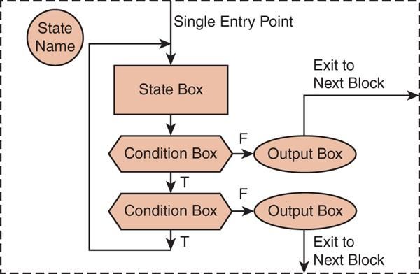
3.1 Introduction 135

•   In 1854 George Boole introduced a systematic treatment of logic and developed for
    this purpose an algebraic system known as symbolic logic, or Boolean algebra.
•   Boolean algebra is a branch of mathematics and it can be used to describe the
    manipulation and processing of binary information. The two-valued Boolean algebra
    has important application in the design of modern computing systems.
•   This chapter contains a brief introduction the basics of logic design. It provides
    minimal coverage of Boolean algebra and this algebra’s relationship to logic gates
    and basic digital circuit.

3.2 Boolean Algebra 136

•   Boolean algebra is algebra for the manipulation of objects that can take on only two
    values, typically true and false.
•   It is common to interpret the digital value 0 as false and the digital value 1 as true.

3.2.1 Boolean Expressions 137

•   Boolean Expression: Combining the variables and operation yields Boolean
    expressions.
•   Boolean Function: A Boolean function typically has one or more input values and
    yields a result, based on these input value, in the range {0, 1}.
•   A Boolean operator can be completely described using a table that list inputs, all
    possible values for these inputs, and the resulting values of the operation.
•   A truth table shows the relationship, in tabular form, between the input values and
    the result of a specific Boolean operator or function on the input variables.
•   The AND operator is also known as a Boolean product. The Boolean expression xy
    is equivalent to the expression x * y and is read “x and y.” The behavior of this
    operator is characterized by the truth table shown in Table 3.1

                           TABLE 3.1 Truth Table for AND

CMPS375 Class Notes (Chap03)           Page 2 / 36                      Dr. Kuo-pao Yang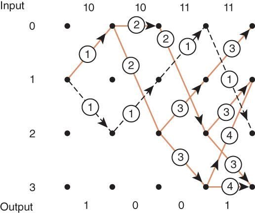
•   The OR operator is often referred to as a Boolean sum. The expression x+y is read
    “x or y”. The truth table for OR is shown in Table 3.2

                             TABLE 3.2 Truth Table OR

•   Both x and x’ are read as “NOT x.” The truth table for NOT is shown in Table 3.3

                          TABLE 3.3 Truth Table for NOT

•   The rule of precedence for Boolean operators give NOT top priority, followed by
    AND, and then OR

                   TABLE 3.4 Truth Table for F(x, y, z) = x + y’z

CMPS375 Class Notes (Chap03)          Page 3 / 36                    Dr. Kuo-pao Yang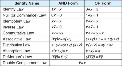
3.2.2 Boolean Identities 138

•   Boolean expression can be simplified, but we need new identities, or laws, that apply
    to Boolean algebra instead of regular algebra.

                   TABLE 3.5 Basic Identities of Boolean Algebra

•   DeMorgan’s law provides an easy way of finding the complement of a Boolean
    function.

          TABLE 3.6 Truth Tables for the AND Form of DeMorgan’s Law

CMPS375 Class Notes (Chap03)           Page 4 / 36                    Dr. Kuo-pao Yang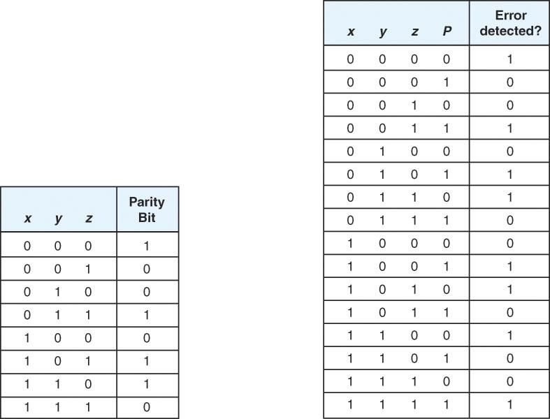
3.2.3 Simplification of Boolean Expressions 140

•   The algebraic identities we studied in algebra class allow us to reduce algebraic
    expression to their simplest form.
•   EXAMPLE Prove that (x + y) (x’ + y) = y.

                                 Example using Identities

•   How did we know to insert additional terms to simplify the function? Unfortunately,
    there no defined set of rules for using these identities to minimize a Boolean
    expression: it is simply something tat comes with experience.
•   To prove the equality of two Boolean expressions, you can also create the truth tables
    for each and compare. If the truth tables are identical, the expressions are equal.

3.2.4 Complements 143

•   F(x, y, z) = x’ + yz’ and its complement, F’(x, y, z) = x(y’ + z)

    TABLE 3.7 Truth Table Representation for a Function and Its Complement

CMPS375 Class Notes (Chap03)             Page 5 / 36                    Dr. Kuo-pao Yang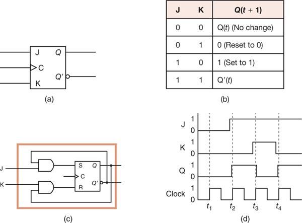
3.2.5 Representing Boolean Functions 144

•   In fact, there are an infinite number of Boolean expressions that are logically
    equivalent to one another.
•   Two expressions that can be represented by the same truth table are considered
    logically equivalent.
•   The two most common standardized forms are the sum-of-products form and the
    product-of-sums form.
•   In the sum-of-products form, ANDed variables are ORed together. For example,

•   In the product-of-sums form, ORed variables are ANDed together. For example,

•   The sum-of-products form is usually easier to work with and to simplify, so we use
    this form exclusively in the sections that follow.
•   It is easy to convert a function to sum-of-products form using its truth table.
•   We are interested in the values of the variables that make the function true (=1).
    Using the truth table, we list the values of the variables that result in a true function
    value.
•   Each group of variables is then ORed together.
•   EXAMPLE 3.9

         TABLE 3.8 Truth Table Representation for the Majority Function
             sum-of-products: F(x, y, z) = x’yz + xy’z + xyz’ + xyz

CMPS375 Class Notes (Chap03)            Page 6 / 36                      Dr. Kuo-pao Yang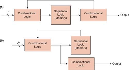
3.3 Logic Gates 146

•   We see that Boolean functions are implemented in digital computer circuits called
    gates.
•   A gate is an electronic device that produces a result based on two or more input
    values.
    o In reality, gates consist of one to six transistors, but digital designers think of
        them as a single unit.
    o Integrated circuits contain collections of gates suited to a particular purpose.

3.3.1 Symbols for Logic Gates 146

•   The three simplest gates are the AND, OR, and NOT gates.

                          FIGURE 3.1 The Three Basic Gates

•   Another very useful gate is the exclusive OR (XOR) gate.
•   The output of the XOR operation is true only when the values of the inputs differ.

                     FIGURE 3.2 The Exclusive OR (XOR) Gate

CMPS375 Class Notes (Chap03)           Page 7 / 36                     Dr. Kuo-pao Yang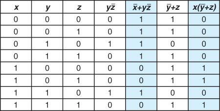
3.3.2 Universal Gates 147

•    Two other common gates are NAND and NOR, which produce complementary
     output to AND and OR.

    FIGURE 3.3 and 3.4 Truth Table and Logic Symbols for NAND and NOR Gates

•    NAND and NOR are known as universal gates because they are inexpensive to
     manufacture and any Boolean function can be constructed using only NAND or only
     NOR gates.

          FIGURE 3.5 Three Circuits Constructed Using Only NAND Gates

3.3.3 Multiple Input Gates 148

•    Gates can have multiple inputs and more than one output.

                    FIGURE 3.6, 3.7, and 3.8 Multiple Input Gates

CMPS375 Class Notes (Chap03)           Page 8 / 36                  Dr. Kuo-pao Yang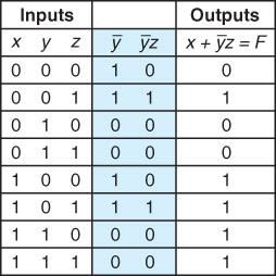
3.4 Karnaugh Maps 149

3.4.1 Introduction 149

•   Minimizing circuits helps reduce the number of components in the actual physical
    implementation.
•   Reducing Boolean expressions can be done suing Boolean identities; however, using
    identities can be very difficult because no rules are given on how or when to use the
    identities, and there is no well-defined set of steps to follow.
•   In this section, we introduce a systematic approach for reducing Boolean expression.

3.4.2 Description of Kmaps and Terminology 149

•   Karnaugh maps, or Kmaps, are graphical way to represent Boolean functions.
•   For example, if there are two input values, x and y, there are four minterms.

FIGURE 3.9 Minterms for Two Variables        FIGURE 3.10 Minterms for Three Variables

•   EXAMPLE 3.10 F(x, y) = xy

CMPS375 Class Notes (Chap03)            Page 9 / 36                    Dr. Kuo-pao Yang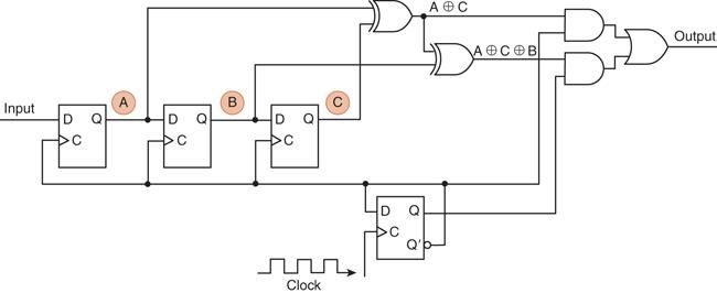
•   EXAMPLE 3.11 F(x, y) = x + y

3.4.3 Kmap Simplification for Two Variables 151

•   The rules of Kmap simplification are:
       1) Groupings can contain only 1s; no 0s.
       2) Only 1s in adjacent cells can be grouped; diagonal grouping is not allowed.
       3) The number of 1s in a group must be a power of 2.
       4) The groups must be made as large as possible while still following all rules.
       5) All 1s must belong a group, even if it is a group of one.
       6) Overlapping groups are allowed.
       7) Wrap around is allowed.
       8) Use the fewest number of groups possible.

                        FIGURE 3.15 Kmap for F(x, y) = x + y

CMPS375 Class Notes (Chap03)          Page 10 / 36                    Dr. Kuo-pao Yang
3.4.4 Kmap Simplification for Three Variables 153
FIGURE 3.16 Minterms and Kmap Format for Three Variables
• EXAMPLE 3.12
It reduces to F(x, y, z) = z
• EXAMPLE 3.13
It reduces to F(x, y, z) = x’ + z’
CMPS375 Class Notes (Chap03) Page 11 / 36 Dr. Kuo-pao Yang3.4.5 Kmap Simplification for Four Variables 156
FIGURE 3.17 Minterms and Kmap Format for Four Variables
• EXAMPLE 3.15
• EXAMPLE 3.16
• The last terms are different. F1 and F2, however, are equivalent.
• If we follow the rules, Kmap minimization results in a minimized function (and thus a
minimal circuit), but these minimized functions need not be unique in representation.
F(w, x, y, z) = F1 = y’z’ + w’yz + w’xz’ F(w, x, y, z) = F2 = y’z’ + w’yz + w’xy
CMPS375 Class Notes (Chap03) Page 12 / 36 Dr. Kuo-pao Yang3.4.6 Don’t Care Conditions 159
• There are certain situations where a function may not be completely specified,
meaning there may be some inputs that are undefined for the function.
• Real circuits don’t always need to have an output defined for every possible input.
• If a circuit is designed so that a particular set of inputs can never happen, we call this
set of inputs a don’t care condition.
• They are very helpful to us in Kmap circuit simplification. Because they are input
values that should not matter (and should never occur), we can let them have values
of either 0 or 1, depending on which helps us the most.
• Don’t care values are typically indicated with an “X” in the appropriate cell.
• EXAMPLE 3.19
3.4.7 Summary 160
• Using Boolean identities for reduction is awkward and can be very difficult.
• Kmaps provide a precise of steps to follow to find the minimal representation of a
function, and thus the minimal circuit that function represents.
• The rules of Kmap simplification are:
1) Groupings can contain only 1s; no 0s
2) Only 1s in adjacent cells can be grouped; diagonal grouping is not allowed.
3) The number of 1s in a group must be a power of 2.
4) The groups must be made as large as possible while still following all rules.
5) All 1s must belong a group, even if it is a group of one.
6) Overlapping groups are allowed.
7) Wrap around is allowed.
8) Use the fewest number of groups possible.
CMPS375 Class Notes (Chap03) Page 13 / 36 Dr. Kuo-pao Yang3.5 Digital Components 160
• Every computer is built using collections of gates that are all connected by way of
wires acting as signal gateway.
3.5.1 Digital Circuits and Their Relationship to Boolean Algebra 160
• More complex Boolean expressions can be represented as combinations of AND, OR,
and NOT gates, resulting in a logic diagram that describes the entire expression.
FIGURE 3.18 A Logic Diagram for F(x, y, z) = x + y’z
3.5.2 Integrated Circuits 162
• Gates are not sold individually; they are sold in units called integrated circuits (ICs).
• A chip (a small silicon semiconductor crystal) is a small electronic device consisting
of the necessary electronic components (transistors, resistors, and capacitors) to
implement various gates.
• The first IC were called SSI chips and contained up to 100 electronic components per
chip.
• We now have ULSI (ultra large-scale integration) with more than 1 million electronic
components per chip.
FIUGRE 3.19 Simple SSI Integrated Circuit
CMPS375 Class Notes (Chap03) Page 14 / 36 Dr. Kuo-pao Yang• Example:
o The Boolean circuit: F(x, y, z) = x’y
o Can be rendered using only NAND gates as:
o So we can wire the pre-packaged circuit to implement our function: F(x, y, z) =
x’y
CMPS375 Class Notes (Chap03) Page 15 / 36 Dr. Kuo-pao Yang3.5.3 Putting It All Together: From Problem Description to Circuit 164
• Boolean logic is used to solve practical problems.
• Expressed in terms of Boolean logic practical problems can be expressed by truth
tables.
• Truth tables can be readily rendered into Boolean logic circuits.
• Example
o Suppose we are to design a logic circuit to determine the best time to plant a
garden. We consider three factors (inputs):
▪ (1) Time, where 0 represents day and 1 represents evening;
▪ (2) Moon phase, where 0 represents not full and 1 represents full; and
▪ (3) Temperature, where 0 represents 45°F and below, and 1 represents over
45°F.
▪ We determine that the best time to plant a garden is during the evening with
a full moon.
o This results in the following truth table:
o From the truth table, we derive the circuit:
CMPS375 Class Notes (Chap03) Page 16 / 36 Dr. Kuo-pao Yang3.6 Combinational Circuits 166
• Digital logic chips are combined to give us useful circuits. These logic circuits can be
categorized as either combinational logic (Section 3.6) or sequential logic (Sec. 3.7).
3.6.1 Basic Concepts 166
• The key concept in recognizing a combinational circuit is that an output is always
based on the given inputs.
• The output of a combinational circuit is a function of its inputs, and the output is
uniquely determined by the values of the inputs at any given moment.
• A given combinational circuit may have several outputs. If so, each output represents
a different Boolean function.
3.6.2 Examples of Typical Combinational Circuits 166
TABLE 3.9 and FIGURE 3.20 Truth Table and Logic Diagram for a Half-Adder
Sum = X xor Y; Carry = XY
• Note that this full-adder is composed of two half-adder
FIGURE 3.21 Truth Table and Logic Diagram for a Full-Adder
Sum = X xor Y xor Cin; Cout = XY + (X xor Y) Cin
CMPS375 Class Notes (Chap03) Page 17 / 36 Dr. Kuo-pao YangFIGURE 3.22 Logic Diagram for a Ripple-Carry Adder
• Decoder: Decoding binary information from a set of n inputs to a maximum of 2n
outputs.
• A decoder uses the inputs and their respective values to select one specific output line.
• One unique output line is set to 1, while the other output lines are set to 0.
• A decoder that has 3 inputs and 8 outputs is called a 3-to-8 decoder.
FIGURE 3.23 a) A Look Inside a Decoder; b) A Decoder Symbol
• EXAMPLE 3.13 A 3-to-8 decoder circuit
o Imagine memory consisting of 8 chips, each containing 8K bytes.
o We have a total of 8K * 8, or 64K (65,536) address available.
o We need 16 bits to represent each address.
o The leftmost 3 bits determine on which chip the address is actually located. All
addresses on chip 0 have the format: 000X XXXX XXXX XXXX: Because chip
0 contains the address 0-8191. Similarly, all addresses on the chip 1 have the
format: 001X XXXX XXXX XXXX.
o The 3 high-order bits are actually used as the inputs to a decoder so the computer
can determine which chip to activate for reading or writing.
o The output of the decoder is used to activate one, and only one, chip as the
addresses are decoded.
CMPS375 Class Notes (Chap03) Page 18 / 36 Dr. Kuo-pao Yang• The Multiplexer circuits binary information from one of many input lines and directs
it to a single output line.
• Only one input (the one selected) is routed through the circuit to output line. All other
inputs are “cut off.”
• Can you think of some situations that require multiplexers? Time-sharing computers
multiplex the input from user terminals. Modem pools multiplex the modem lines
entering the computer.
FIGURE 3.24 a) A Look Inside a Multiplexer; b) A Multiplexer Symbol
• A parity generator is a circuit that creates the necessary parity bit to add to a word.
• A parity checker checks to make sure proper parity (odd or even) is present in the
word.
• Typically, parity generators and parity checkers are constructed using XOR functions.
Assuming we are using odd parity, the truth table for a parity generator for a 3-bit
word is given in Table 3.11.
• The parity checker outputs a 1 if an error is detected and 0 otherwise.
Table 3.10 Parity Generator Table 3.11 Parity Checker
CMPS375 Class Notes (Chap03) Page 19 / 36 Dr. Kuo-pao Yang• Bit shifting, moving the bits of a word or byte one position to the left or right is a
useful operation.
• When the bits of an unsigned integer are shifted to the left by one position, it has the
same effect as multiplying that integer by 2.
• The leftmost or rightmost bit is lost after a left or right shift (respectively).
• Left shifting the nibble, 0110 (610), change it to 1100 (1210), and right shifting it
produces 0011 (310).
FIGURE 3.25 4-Bit Shifter
• When the control line, S, is low, each bit of the input (labeled I0 to I3) is shift left by
one position into the outputs (Labeled O0 through 03).
• When the control line, S, is high, each bit of the input (labeled I0 to I3) is shift right
occurs.
CMPS375 Class Notes (Chap03) Page 20 / 36 Dr. Kuo-pao Yang• Figure 3.26 illustrates a very simple ALU with four basic operations – AND, OR,
NOT, and addition – carried out on two machine words of 2 bits each.
• The control lines, f0, and f1, determine which operation is to be performed by the CPU.
• The signal 00 (f0 f1) is used for addition (A + B); 01 for NOT A; 10 for A OR B, and
11 for A AND B.
• The input lines A0 and A1 indicate 2 bits of one word, while B0 and B1 indicate the
second word, C0 and C1 represent the output lines.
FIGURE 3.26 A Simple Two-Bit ALU
CMPS375 Class Notes (Chap03) Page 21 / 36 Dr. Kuo-pao Yang3.7 Sequential Circuits 175
• The major weakness of combinational circuits is that there is no concept of
storage – they are memoryless. If we change an input value, this has a direct and
immediate impact on the value of the output.
3.7.1 Basic Concepts 176
• A sequential circuit defines its output as a function of both its current inputs and its
previous inputs. Therefore, the output depends on past inputs.
• We typically refer to this storage element as a flip-flop.
• Combinational circuits are generalizations of gates; sequential circuits are
generalizations of flip-flops.
3.7.2 Clocks 176
• A sequential circuit uses past inputs to determine present outputs indicates we must
have event ordering.
• A clock is a circuit that emits a series of pulses with a precise pulse width and a
precise interval between consecutive pulses.
• This interval is called the clock cycle time. Clock speed is generally measured in
megahertz (MHz), or gigahertz (GHz).
• A clock is used by a sequential circuit to decide when to update the state of the
circuit.
• Most sequential circuits are edge-triggered (as opposed to being level-triggered). It
means they are allowed to change their state on either the rising or falling edge of the
clock signal.
FIGURE 3.28 A clock Signal Indicating Discrete Instances of Time
CMPS375 Class Notes (Chap03) Page 22 / 36 Dr. Kuo-pao Yang3.7.3 Flip-Flops 176
• Many people use the terms latch and flip-flop interchangeably. Technically, a latch is
level triggered, whereas a flip-flop is edge triggered.
• In order to “remember” a past state, sequential circuits rely on a concept called
feedback. This simply means the output of a circuit is fed back as an input to the
same circuit.
FIGURE 3.29 Example of Simple Feedback
• A more useful feedback circuit is composed of two NOR gates resulting in the most
basic memory unit call an SR flip-flop. SR stands for “set/reset.”
FIGURE 3.30 A SR Flip-Flop Logic Diagram
CMPS375 Class Notes (Chap03) Page 23 / 36 Dr. Kuo-pao Yang• Q(t) means the value of the output at time t. Q(t+1) is the value of Q after the next
clock pulse.
• When both S and R are 1, the SR flip-flop is unstable.
FIGURE 3.31 (a) SR Flip-Flop
(b) Clocked SR Flip-Flop
(c) Characteristic Table for the SR Flip-Flop
(d) Timing Diagram for the SR Flip-Flop (assuming the initial state of Q is 0)
• The SR flip-flop actually has three inputs: S, R, and its current output, Q.
TABLE 3.12 Truth Table for SR Flip-Flop
CMPS375 Class Notes (Chap03) Page 24 / 36 Dr. Kuo-pao Yang• A JK flip-flop simply modify the SR flip-flop to ensure that the illegal state (both S
and R are 1) never arises.
• The inputs to an SR flip-flop will never both be 1
• We will never have an unstable circuit.
FIGURE 3.32 (a) JK Flip-Flop
(b) JK Characteristic Table
(c) JK Flip-Flop as a Modified SR Flip-Flop
(d) Timing Diagram for JK Flip-Flop (assuming the initial state of Q is 0)
CMPS375 Class Notes (Chap03) Page 25 / 36 Dr. Kuo-pao Yang• A D flip-flop is a true representation of physical computer memory.
• An output value of 1 means the circuit is currently “storing” a value of 1.
FIGURE 3.33 (a) D Flip-Flop
(b) D Flip-Flop Characteristic Table
(c) D Flip-Flop as a Modified SR Flip-Flop
(d) Timing Diagram for D Flip-Flop
CMPS375 Class Notes (Chap03) Page 26 / 36 Dr. Kuo-pao Yang3.7.4 Finite-State Machines 180
• The behavior of sequential circuits can be expressed using characteristic tables or
finite state machines (FSMs).
o FSMs typically use circles to represent a set of machine states and directed arcs to
represent transitions from one state to another.
o FSMs can be in only one state at a time.
• Moore and Mealy machines are two types of FSMs that are equivalent.
o They differ only in how they express the outputs of the machine.
• Moore machines place outputs on each node, while Mealy machines present their
outputs on the transitions.
• For Example, the behavior of a JK flop-flop is depicted below by a Moore machine
(left) and a Mealy machine (right).
o This implies that a Mealy machine’s outputs are a function of its current state and
its input, and a Moore machine’s output is a function only of its current state.
FIGURE 3.34 JK Flip-Flop Represented as a Moore Machine (Left)
FIGURE 3.36 JK Flip-Flop Represented as a Mealy Machine (Right)
• In the actual implementation of either a Moore or Mealy machine, two things are
required: a memory (register) to store the current state and combinational logic
components that control the output and transitions from one state to another.
FIGURE 3.37 (a) Block Diagram for Moore Machines
(b) Block Diagram for Mealy Machines
CMPS375 Class Notes (Chap03) Page 27 / 36 Dr. Kuo-pao Yang• It is difficult to express the complexities of actual implementations using only Moore
and Mealy machines.
o For one thing, they do not address the intricacies of timing very well.
o Secondly, it is often the case that an interaction of numerous signals is required to
advance a machine from one state to the next.
• For these reasons, Christopher Clare invented the algorithmic state machine (ASM).
o An algorithmic state machine consists of blocks that contain a state box, a label,
and optionally condition and output boxes.
o Each ASM block has exactly one entry point and at least one exit point.
FIGURE 3.38 Components of an Algorithmic State Machine
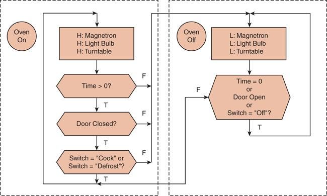
• An ASM for a microwave oven example
FIGURE 3.39 Algorithmic State Machine for a Microwave Oven
CMPS375 Class Notes (Chap03) Page 28 / 36 Dr. Kuo-pao Yang3.7.5 Examples of Sequential Circuits 188
• The registers must all accept their new input values and change their storage elements
at the same time.
FIGURE 3.40 a) 4-Bit Register; b) Block Diagram for a 4-Bit Register
• If we begin counting in binary: 0000, 0001, 0010, 0011, ..., 1111, we can see that as
the numbers increase, the low-order bit is complemented each time.
• When J and K are both equal to 1, the flip-flop complements the present state.
• The circuit counts only when the clock pulses and this count enable line is set to 1.
FIGURE 3.41 4-Bit Synchronous Counter Using JK Flip-Flops
CMPS375 Class Notes (Chap03) Page 29 / 36 Dr. Kuo-pao Yang• The memory depicted holds four 3-bit words (4 X 3 memory).
• A read or write operation always reads or writes a complete word.
• The input In0, In1, In2 are lines used to store, or write, a 3-bit word to memory.
• The lines S0 and S1 are the address lines used to select which word in memory is
being referenced (Notice that S0 and S1 are the input lines to a 2-to-4 decoder that is
responsible for selecting the correct memory word.)
• The output lines (Out0, Out1, and Out2) are used when reading words from memory.
• The write enable control line indicates whether we are reading or writing.
• In practice, the input lines and output lines are the same lines.
• To summarize our discussion of this memory circuit, here are the steps necessary to
write a word to memory:
1) An address is asserted on S0 and S1.
2) WE (write enable) is set to high
3) The decoder using S0 and S1 enables only one AND gate, selecting a given
word in memory
4) The line selected in Step 3 combined with the clock and WE select only one
word
5) The write gate enabled in Step 4 drives the clock for the selected word.
6) When clock pulses, the word on the input lines is loaded into the D flip-flops.
FIGURE 3.42 4 X 3 Memory
CMPS375 Class Notes (Chap03) Page 30 / 36 Dr. Kuo-pao Yang3.7.6 An Application of Sequential Logic: Convolutional Coding and
Viterbi Detection 194
• Convolutional coding is a method that operates on an incoming serial bit stream,
generating an encoded serial output stream (including redundant bits) that enables it
to correct errors continuously. A convolutional code is an encoding process whereby
the output is a function of the input and some number of bits previously received.
• A Viterbi decoder reads the bits that have been output by a convolutional encoder
and compares the symbol stream read with a set of “probable” symbol streams. The
one with the least error is selected for output.
• Convolutional encoding combined with Viterbi decoding has become an accepted
industry standard for encoding and decoding data stored or transmitted over imperfect
(noisy) media.
• The convolutional coding mechanism used in PRML is illustrated in Figure 3.43.
o Two output bits are written for each input bit.
o The first output bit is a function of the input bit and the second previous input bit:
A XOR C. The second bit is a function of the input bit and the two previous bits:
A XOR C XOR B.
o The two AND gates at the right-hand side of the diagram alternatively select one
of these functions during each pulse of the clock.
o The input is shifted through the D flip-flops on every second clock pulse.
FIGURE 3.43 Convolutional Encoder for PRML
TABLE 3.13 Characteristic Table for the Convolutional Encoder in Figure 3.43
CMPS375 Class Notes (Chap03) Page 31 / 36 Dr. Kuo-pao Yang• The characteristic table for this circuit is given in Table 3.13. As an example,
consider the stream of input bits, 11010010. The encoder initially contains all 0s, so B
= 0 and C = 0. The output of the completed encoder function is
F (1101 0010) = 11 01 01 00 10 11 11 10
• The encoding process is made a little clearer using the Mealy machine (Figure 3.45).
FIGURE 3.45 Mealy Machine for the Convolutional Encoder in Figure 3.43
• By reversing the inputs with the outputs on the transition arcs, as shown in Figure
3.46, we place bounds around the set of possible decoding inputs.
FIGURE 3.46 Mealy Machine for a Convolutional Decoder
CMPS375 Class Notes (Chap03) Page 32 / 36 Dr. Kuo-pao Yang• A Viterbi detector uses the logical equivalent of paths through this diagram to
determine the most likely bit pattern.
• In Figure 3.47, the input sequence 00 10 11 11 is encountered with the decoder
starting in State 1. You can compare the transitions in the trellis diagram with the
transitions in the Mealy diagram in Figure 3.46.
FIGURE 3.47 Trellis Diagram Illustrating State Transitions
for the Sequence 00 10 11 11
• Suppose we introduce an error in the first pair of bits in our input, giving the
erroneous string 10 10 11 11. With our decoder starting in State 1, Figure 3.48 traces
the possible paths through the trellis. The accumulated Hamming distance is shown
on each of the transition arcs. The correct path that correctly assumes that the string
should be 00 10 11 11 is the one having the smallest accumulated error, so it is
accepted as the correct sequence.
FIGURE 3.48 Trellis Diagram Illustrating Hamming Errors
for the Sequence 10 10 11 11
CMPS375 Class Notes (Chap03) Page 33 / 36 Dr. Kuo-pao Yang3.8 Designing Circuits 199
• Digital logic design requires not only familiar with digital logic, but also versed in
o digital analysis (analyzing the relationship between inputs and outputs),
o digital synthesis (starting with a truth table and determining the logic diagram to
implement the given logic function), and
o the use of CAD (computer-aided design) software.
• A circuit designer faces many problems, including:
o finding efficient Boolean functions,
o using the smallest number of gates,
o using an inexpensive combination of gates,
o organizing the gates of a circuit board to use the smallest surface area and
minimal power requirements, and
o attempting to do all of this using a standard set of modules for implementation.
• Digital systems designers must also be mindful of the physical behaviors of circuits to
include minute propagation delays that occur between the time when a circuit’s
inputs are energized and when the output is accurate and stable.
• There are many tools available to help with the design of digital logic circuits.
o These are hardware computer languages (HDLs) that allow for a top-down
methodology resulting in a precise and formal description of digital circuits.
o HDLs not only increase productivity and flexibility, but also allow for quick
changes and design reuse.
o The designer can use an HDL to simulate the circuit before actually building it.
o Unlike regular programs describe algorithms, HDLs describe hardware structures.
• Two very popular HDLs are VHDL and Verilog. VHDL (VHSIC Hardware
Description Language, where VHSIC stands for Very High Speed Integrated Circuit)
was developed in the early 1980s.
o Every VHDL program contains at least one entity/architecture pair.
o In addition, each program should contain an architecture declaration describing
the actual function of the entity. As an example, consider the following VHDL
code to specify the behavior of an AND gate:
CMPS375 Class Notes (Chap03) Page 34 / 36 Dr. Kuo-pao Yango This code first defines a signal and_gate of type std_logic that is assigned
two inputs. The inputs are defined in the entity andGate, which contains three
signals: input1, input2, and res_out. The architecture func describes the
functionality of the entity andGate.
• Verilog performs a similar task, but has a completely different structure from VHDL.
o Verilog allows you to design in a more modular fashion, allowing the
programmer to use system blocks called modules.
o Each module specifies the input signals, the output signals, and the internal
structure and behavior of the circuit being designed. The following is Verilog
code to define a half-adder:
o The Verilog ^ operator performs an exclusive OR, while the & operator performs
an AND. If you compare this to the half-adder in Figure 3.20, you can see how
the code corresponds to the actual circuit.
• A circuit designer can implement any given algorithm in hardware (recall the
Principle of Equivalence of Hardware and Software from chapter 1).
• Embedded Systems
o When we need to implement a simple, specialized algorithm and its execution
speed must be as fast as possible; a hardware solution is often preferred.
o This is the idea behind embedded systems, which are small special-purpose
computers that we find in many everyday things. Your microwave oven and your
car most likely contain embedded systems.
o Programming these embedded systems required design software that can read
input variables and send output signals to perform such tasks as turning a light
on or off, emitting a beep, sounding an alarm, or opening a door.
o Embedded systems require special programming that demands an understanding
of the operation of digital circuits, the basics of which you have learned in this
chapter.
CMPS375 Class Notes (Chap03) Page 35 / 36 Dr. Kuo-pao YangChapter Summary 201
• Computers are implementations of Boolean logic.
• Any Boolean functions can be represented as truth tables.
• Truth tables provide us with a means to express the characteristics of Boolean
functions as well as logic circuits.
• There is a one-to-one correspondence between a Boolean function and its digital
representation.
• From a chip designer’s point of view, the two most important factors are speed and
cost: minimizing the circuits helps to both lower the cost and increase performance.
• Computer circuits consist of combinational logic circuits and sequential logic
circuits.
• Combinational circuits produce outputs (almost) immediately when their inputs
change.
• Sequential circuits require clocks to control their changes of state.
• Combinational logic devices, such as adders, decoders, and multiplexers, produce
outputs that are based strictly on the current inputs.
• The AND, OR, and NOT gates are the building blocks for combinational logic
circuits, although universal gates, such as NAND and NOR, could also be used.
• Sequential logic devices, such as registers, counters, and memory, produce outputs
based on the combination of current inputs and the current state of the circuits. These
circuits are built using SR, D, and JK flip-flops.
• The behavior of sequential circuits can be expressed using characteristic tables or
through various finite state machines.
• Moore and Mealy machines are two finite state machines that model high-level
circuit behavior.
• Algorithmic state machines are better than Moore and Mealy machines at expressing
timing and complex signal interactions.
• Examples of sequential circuits include memory, counters, and Viterbi encoders and
decoders.
• Two very popular HDLs are VHDL and Verilog to help with the design of digital
logic circuits.
CMPS375 Class Notes (Chap03) Page 36 / 36 Dr. Kuo-pao YangYou can also read