FEW-ELECTRON SINGLE AND DOUBLE QUANTUM DOTS IN AN INAS TWO-DIMENSIONAL ELECTRON GAS
←
→
Page content transcription
If your browser does not render page correctly, please read the page content below

PRX QUANTUM 2, 010321 (2021)
   Editors’ Suggestion

             Few-Electron Single and Double Quantum Dots in an InAs Two-Dimensional
                                           Electron Gas
             Christopher Mittag,1,* Jonne V. Koski,1 Matija Karalic,1 Candice Thomas ,2,3 Aymeric Tuaz,2,3
            Anthony T. Hatke,2,3 Geoffrey C. Gardner,2,3 Michael J. Manfra,2,3 Jeroen Danon ,4 Thomas Ihn ,1
                                                  and Klaus Ensslin 1
                     1
                    Department of Physics, Solid State Physics Laboratory, ETH Zurich, 8093 Zurich, Switzerland
             2
              Microsoft Station Q Purdue and Department of Physics and Astronomy, Purdue University, West Lafayette,
                                                        Indiana 47907, USA
                       3
                         Birck Nanotechnology Center, Purdue University, West Lafayette, Indiana 47907, USA
          4
            Department of Physics, Center for Quantum Spintronics, Norwegian University of Science and Technology, 7491,
                                                        Trondheim, Norway

                  (Received 15 July 2020; revised 24 November 2020; accepted 25 January 2021; published 9 February 2021)

                    Most proof-of-principle experiments for spin qubits have been performed with GaAs-based quantum
                 dots because of the excellent control they offer over tunneling barriers and the orbital and spin degrees of
                 freedom. Here we present the first realization of high-quality single and double quantum dots hosted in
                 an InAs two-dimensional electron gas, demonstrating accurate control down to the few-electron regime,
                 where we observe a clear Kondo effect and singlet-triplet spin blockade. We measure an electronic g
                 factor of 16 and a typical magnitude of the random hyperfine fields on the quantum dots of approximately
                 0.6 mT. We estimate the spin-orbit length in the system to be approximately 5 − 10 μm (which is almost 2
                 orders of magnitude longer than typically measured in InAs nanostructures), achieved by a very symmetric
                 design of the quantum well. These favorable properties put the InAs two-dimensional electron gas on the
                 map as a compelling host for studying fundamental aspects of spin qubits. Furthermore, having weak spin-
                 orbit coupling in a material with a large Rashba coefficient potentially opens up avenues for engineering
                 structures with spin-orbit coupling that can be controlled locally in space and/or time.

                 DOI: 10.1103/PRXQuantum.2.010321

                         I. INTRODUCTION                                host material [2–5]. The fact that this problem is intrin-
                                                                        sic for GaAs was one of the reasons for a recent shift of
   Electron spins hosted in semiconductor quantum dots
                                                                        focus toward Si- and Ge-based quantum dots, where the
are a compelling platform for quantum information pro-
                                                                        most abundant isotopes have zero nuclear spin. Although
cessing [1], and two-dimensional electron gases (2DEGs)
                                                                        progress has been impressive in recent years [6–12], elec-
formed in GaAs/(Al,Ga)As heterostructures have been
                                                                        trons in these materials have an additional valley degree of
the workhorse of this field for many years. Because of
                                                                        freedom that is difficult to control and can interfere with
the excellent gating technologies in this material system,
                                                                        qubit operation [13].
few-electron quantum dots can be routinely realized with
                                                                           An attractive alternative host system for studying fun-
occupation control down to the last electron, promising,
                                                                        damental aspects of spin qubits could be the InAs-based
in principle, good scalability that is compatible with stan-
                                                                        2DEG. Although both In and As carry nonzero nuclear
dard fabrication techniques. The main obstacle to further
                                                                        spin, the bulk electronic g factor in InAs is approximately
progress in the field of GaAs-based spin qubits is the fast
                                                                        30 times larger than in GaAs, yielding much smaller effec-
decoherence caused by the hyperfine coupling of the elec-
                                                                        tive nuclear fields for comparable hyperfine coupling and
tron spins to the randomly fluctuating nuclear spins in the
                                                                        quantum dot dimensions. Apart from that, the small effec-
                                                                        tive mass m∗ ≈ 0.023m0 in the conduction band of InAs
  *
      mittag@phys.ethz.ch                                               eases the demands on lithographic precision, coming with
                                                                        the additional advantage that a larger quantum dot size
Published by the American Physical Society under the terms of
                                                                        reduces the rms value of the random nuclear fields even
the Creative Commons Attribution 4.0 International license. Fur-
ther distribution of this work must maintain attribution to the         further.
author(s) and the published article’s title, journal citation, and         The reason why the InAs-based 2DEG has not yet
DOI.                                                                    become a leading platform for spin-qubit implementations

2691-3399/21/2(1)/010321(11)                                     010321-1               Published by the American Physical Society
CHRISTOPHER MITTAG et al.                                                               PRX QUANTUM 2, 010321 (2021)

is twofold: First, the sidewalls of etched InAs structures       decoherence and spin-mixing mechanisms, which in prac-
usually contain an accumulation layer of electrons, likely       tice were considered to be intrinsic features in InAs-based
caused by Fermi level pinning [14–17]. The traditional           devices.
mesa etch technique commonly used in GaAs can thus                  Secondly, having a 2DEG with weak spin-orbit cou-
not be applied, as the trivial edge states always short the      pling in a material with a large Rashba coefficient presents
electron gas underneath the gates traversing the mesa. Sec-      conceptually a plethora of new possibilities. In such a
ond, InAs has a large Rashba spin-orbit coefficient [18,19],       material, gate-induced electric fields are capable of gen-
which can leverage small asymmetries in the confining             erating strong spin-orbit interaction locally in space and/or
potential into strong in-plane spin-orbit coupling. This         time. In the context of spin qubits, one could thus imag-
resulted in a surge in interest in InAs-based devices after it   ine using a stacked-gate technology to switch on and off
was pointed out that strong spin-orbit interaction in com-       spin-orbit interaction locally on a quantum dot: Switch-
bination with proximity-induced superconductivity could          ing it on allows fast spin manipulation and switching
result in a topological state hosting zero-energy Majorana       it off could result in a long coherence time, thereby
modes at its boundaries [20–23], which potentially could         combining the best of the two worlds of strong and
be used for topologically protected quantum computation          weak spin-orbit coupling. Furthermore, adding the ingre-
[24,25]. Most experiments in this field rely on wirelike          dient of induced superconductivity to a 2DEG with a
devices, since they allow superconductors to be more eas-        gate-designable spin-orbit landscape could yield a conve-
ily coupled to or even epitaxially grown on them [26–28],        nient platform for creating and braiding Majorana bound
but a planar setup would enable the application of top-          states.
down technology for the fabrication of complex quantum              The rest of this paper is outlined as follows. We begin by
circuits [29]. In the context of spin qubits, however, strong    introducing the details of the heterostructure, the device,
spin-orbit coupling is not necessarily beneficial: although       and its fabrication. In the next section, we form and
it does allow fast electron dipole spin resonance, in general    characterize a single few-electron quantum dot. In an in-
it reduces qubit coherence and compromises qubit control         plane magnetic field we identify the spin of electronic
[30–33].                                                         states from the energy shift of the resonances visible in
   Here we present the first realization of high-quality          finite-bias spectroscopy and analyze the spin-orbit inter-
single and double quantum dots using a split-gate tech-          action on the basis of the crossing of spin singlet and
nology on a planar InAs quantum well, demonstrating              spin triplet states. Completing the experiments on the sin-
electron occupation control down to the last electron and a      gle quantum dot, we increase the tunnel coupling to the
Kondo effect and spin blockade with qualities comparable          leads and observe the Kondo effect in the single-electron
to those of the best GaAs-based samples. We circumvent           regime; its dependences on bias voltage, magnetic field,
the issue of edge conductance by using multiple layers of        and temperature are analyzed. The next section comprises
electrostatic gates [34] and we suppress the Rashba spin-        experiments on the coupling of two neighboring quantum
orbit interaction by covering the InAs well with epitaxial       dots to form a double quantum dot. Singlet-triplet spin
(Al,Ga)Sb barriers, yielding a very symmetric electric field      blockade by Pauli exclusion is observed and characterized.
across the quantum well [35]. We report a g factor of            Studying the leakage current at strong interdot tunnel cou-
approximately 16 and a rms value of approximately 0.6 mT         pling allows us to estimate the strength of the spin-orbit
for the random hyperfine fields on the quantum dots, which         interaction, showing that it is much weaker than reported
is roughly 1 order of magnitude smaller than the typical         for other InAs-based devices. Finally, we reduce the inter-
fields in GaAs-based quantum dots [36,37]. We further             dot tunnel coupling and use the narrow resonance in the
estimate the spin-orbit length lSO in our 2DEG in two inde-      leakage current around zero magnetic field to estimate the
pendent ways, showing that lSO ∼ 5 − 10 μm, which is of          typical magnitude of the nuclear fields on the two quantum
the same order of magnitude as in typical GaAs devices           dots.
[38]. This is unusually long for a lower-dimensional InAs-
based structure and indicates that the Rashba contribution
                                                                                  II. DEVICE DETAILS
is strongly suppressed.
   The implications for the field of quantum technolo-               The heterostructure used in this experiment is grown
gies are manifold. First of all, we put the InAs 2DEG            by molecular beam epitaxy on an undoped GaSb sub-
on the map as a new compelling platform for quantum-             strate wafer in (100) crystal orientation. The main layers
dot-based spin-qubit implementations, having the afore-          of importance for this work can be seen in the schematic
mentioned benefits of a larger g factor and smaller               cross section in Fig. 1(a). They comprise a 24-nm-wide
effective mass as compared with the commonly used                 InAs quantum well [lower blue layer in Fig. 1(a)] sand-
GaAs. The discovery that our symmetric heterostructure           wiched between two 20-nm-wide Al0.8 Ga0.2 Sb barriers
design indeed leads to an almost complete suppression of         (red) and capped with a 1.5-nm InAs layer (upper blue
the Rashba effect removes most of the spin-orbit-related          layer). The quantum well hosts a 2DEG with mobility μ =

                                                           010321-2
FEW-ELECTRON SINGLE AND DOUBLE QUANTUM. . .                                                 PRX QUANTUM 2, 010321 (2021)

(a)                              (b)            PGL1 PGR1               The scanning electron micrograph in Fig. 1(b) shows the
                                          LB1      MB1  RB1          fine gate structure used to define single and double quan-
                                                                     tum dots of a sample similar to the one used in this study.
                                                                     The left quantum dot is defined by the left tunnel barriers
        InAs                           200 nm
        (Al,Ga)Sb                                                    (labeled LB1 and LB2), the left plunger gates (PGL1 and
        InAs                              LB2      MB2  RB2
        (Al,Ga)Sb                               PGL2 PGR2            PGL2), and the middle tunnel barriers (MB1 and MB2).
        Substrate                                                    The latter gates form the right quantum dot together with
(c)                              (d)                dc               the right plunger gates (PGR1 and PGR2) and the right
                                                                     tunnel barriers (RB1 and RB2). The measurements in this
                                                                     paper were conducted in a dilution refrigerator at the base
                                                                     temperature T = 57 mK with use of low-frequency ac
                                                                     lock-in techniques. The frame gate is kept at a negative
                                  dc

                                                                     voltage such that it depletes the 2DEG underneath and
                                                                     electronic transport is measured strictly in the inner part
                                                                     of the electron gas across the quantum dot structure. This
                                                                     is necessary to avoid spurious effects of conduction along
                                                                     the sample edges that were found in similar InAs devices
FIG. 1. (a) Three-dimensional view of sample geometry with a         [14–16,34].
cross section of the heterostructure used. The 24-nm-wide InAs
quantum well (lower blue layer) is sandwiched by two 20-nm
(Al,Ga)Sb barriers (red) and capped with a 1.5-nm InAs layer
(upper blue layer). Multiple layers of gates separated by Al2 O3                 III. SINGLE QUANTUM DOT
dielectric layers create a device used to form single and double
                                                                        In the first experiment, we use the three leftmost gate
quantum dots. (b) Scanning electron micrograph of the gate lay-
out of a device similar to the one used in this study. (c) Coulomb
                                                                     pairs in Fig. 1(b) and apply a negative potential to them to
resonances in the conductance G through the left quantum dot         define the left quantum dot. In the plot of the conductance
as a function of VPGL . (d) Coulomb blockade diamond visible         G measured across the quantum dot as a function of VPGL ,
in the differential conductance as a function of VPGL and Vdc .       the voltage applied to the left plunger gates, we observe
Uninterrupted Coulomb resonances up to Vdc = ±10 mV and the          narrow Coulomb resonances. Two of these are shown in
absence of additional resonances indicate the loading of the first    Fig. 1(c), and each indicates the change of the quantum dot
electron.                                                            occupancy by one electron. We tune the system into a state
                                                                     where we presume these to be the last two electrons on the
                                                                     quantum dot. As this sample does not have a nearby charge
1.4 × 106 cm2 V−1 s−1 at density ne = 5.1 × 1011 cm−2                detector [40,41] we present the results of multiple experi-
measured at temperature T = 1.5 K. Further details on                ments in the following that all consistently confirm that
hetereostructure growth and properties can be found in               this is the case. The results of one of these experiments are
Ref. [39].                                                           displayed in Fig. 1(d), where we record the differential con-
   To fabricate the device, Ti(20 nm)/Ni(20 nm)/Au(100               ductance as a function of VPGL and a dc source-drain bias
nm) Ohmic contacts are deposited in the first step. This is           voltage Vdc up to ±10 mV, much larger than the charging
followed by the growth of 20-nm Al2 O3 by atomic layer               energy of the quantum dot. Past the last Coulomb block-
deposition at 150◦ C as a first gate dielectric, on top of            ade diamond, no additional resonances appear, while the
which the Ti(5 nm)/Au(45 nm) rectangular frame gate is               resonances that indicate the charging of the quantum dot
deposited. Subsequently, a second gate dielectric of 20-nm           with the first electron remain visible. This implies that the
Al2 O3 is deposited in analogy to the previous step. This            lack of additional resonances is not caused by the closing
enables the deposition of Ti(10 nm)/Au(50 nm) gate leads             tunnel barriers.
and Ti(5 nm)/Au(20 nm) fine gates defined by optical and
electron beam lithography, respectively. In a last step, the
contacts are released with a hydrofluoric acid etch of the                          A. Excited-state spectroscopy
dielectric layer in the contact areas and carefully con-                For the next measurement, we tune the quantum dot
tacted by glueing bond wires with conductive epoxy to                such that we observe the Coulomb blockade diamonds of
prevent any leakage to the GaSb substrate wafer that could           the first two electrons. These are shown in Fig. 2(a), where
be caused by wire bonding. Fabrication on such shallow               we again record the differential conductance as a function
2DEGs with Fermi level pinning at the surface is delicate            of VPGL and Vdc . Integer numbers indicate the quantum dot
and the yield is lower than with standard mesa-etch tech-            occupancy. At bias voltage Vdc = ±3.9 mV, we find res-
niques. A schematic overview of this structure can be seen           onances of excited states branching off the two-electron
in Fig. 1(a).                                                        Coulomb blockade diamond. In two-electron quantum dots

                                                              010321-3
CHRISTOPHER MITTAG et al.                                                                      PRX QUANTUM 2, 010321 (2021)

 (a)                                      (c)                          “S” and “T” cross. Resonance S appears where the tran-
                                                                       sition energy ↑ → S equals the chemical potential μS of
                                 dc               dc

                                                                       the source lead, and resonance T occurs where the energy
                                                                       of both ↑ → T+ and ↓ → T0 match μS . Thus, at the point
            0    1           2                                         where resonances S and T cross, the two-electron S and
                                                                       T+ states are degenerate, and past this crossing, the ground
   dc

                                                                       state of the two-electron system turns from a spin singlet
                                                                       to a spin triplet [45]. This region of proximity between
                                                                       these two states has been thoroughly investigated in quan-
 (b)                                      (d)                          tum dots formed in InAs nanowires, as the magnitude of
                                 dc               dc                   the anticrossing observed there is indicative of the strength
                                                                       of the spin-orbit interaction in the quantum dot [30,31].
                                                                       The data in this region in our quantum dot defined in a
                                                                       2DEG can be seen in Fig. 2(d). In contrast to the quantum
                         S   T
                                                                       dots defined in nanowires, we cannot detect a clear spin-
        0            1                2
                                                                       orbit-mediated anticrossing of singlet and triplet states
                                                 S     T               within our experimental resolution. Converting VPGL to
                                                                       an energy scale using the Zeeman splitting between the
                                                                       single-electron spin-up and spin-down resonances that are
                                                                       visible on the left side of Fig. 2(b), we estimate that the size
FIG. 2. (a) Coulomb blockade diamonds corresponding to the
                                                                       of the anticrossing does not exceed approximately 80 μeV.
loading of the first two electrons. A resonance corresponding to
the transition to an excited state branches off the two-electron        Under the assumption that the magnitude of this   √spin-orbit-
Coulomb blockade diamond at Vdc = −3.9 mV. (b) Magnetic                induced anticrossing is roughly |g ∗ μB B |r/ 2lSO [30],
field dependence of the resonances along the dashed white               where r is the average distance between the two electrons
line in (a). (c) Enlargement of the dashed yellow box in (b).          occupying the quantum dot, we can estimate the relevant
A linear Zeeman splitting of the resonances corresponding to           spin-orbit length in the quantum dot to be approximately
the loading of the first electron is visible. (d) Enlargement the       0.9 μm or greater, assuming that r ∼ 30 nm.
dashed blue box in (b), where a direct crossing of the reso-              This corresponds to a rather weak spin-orbit coupling
nances corresponding to the spin singlet and a spin triplet state is   compared with other reported values for InAs-based sys-
observed.
                                                                       tems [19,30,31,46]. To understand the relatively weak
                                                                       spin-orbit coupling we observe, we consider the various
in GaAs, the ground state is usually believed to be the spin-          contributions separately: (i) The Dresselhaus contribution
singlet state, whereas this lowest excitation is associated            [47] to the spin-orbit interaction depends on crystal inver-
with the threefold-degenerate spin-triplet state [42].                 sion asymmetry, and its strength in InAs is comparable
   To further elucidate the spin of these excited states, as           to that in GaAs [18]. Because of the difference in effec-
well as to corroborate our hypothesis of the occupancy                 tive mass, the associated spin-orbit length will be 3 times
of this few-electron quantum dot, we use a parallel mag-               longer than in a comparable GaAs-based system and thus
netic field while varying the plunger gate voltage along                can be roughly estimated to be on the order of 3–30 μm.
the dashed white line in Fig. 2(a) at a finite bias volt-               The expected strength of the Dresselhaus contribution is
age Vdc = −3.9 mV. The resulting data for the differential              thus not inconsistent with the estimate given above. (ii)
conductance as a function of VPGL and the magnetic field                The coefficient of the Rashba contribution, which deter-
B are shown in Fig. 2(b). Here we note a linear Zeeman                mines the strength of the spin-orbit coupling arising from
splitting of all resonances. To better visualize the split-            structural inversion asymmetry of the system, is much
ting of the first visible resonance, we show in Fig. 2(c)               larger in InAs than in GaAs. Nevertheless, the Rashba-
an enlargement of the dashed yellow box in Fig. 2(b). As               type spin-orbit interaction in the 2DEG depends not only
expected for the first electron, we recognize a linear split-           on this coefficient but also on the electric field normal to
ting into two resonances for the two spin projections. From            the plane of the 2DEG. The large and tunable spin-orbit
the magnitude of the splitting, we extract an effective g fac-          interaction that was attributed to InAs 2DEGs in previ-
tor of |g ∗ | = 16.4, which is comparable to the bulk value            ous experiments was achieved by use of very asymmetric
expected for InAs [43,44].                                             quantum wells and strong electric fields perpendicular to
                                                                       the quantum well [19,46]. Here, on the other hand, the
                                                                       quantum well is wide and contained by symmetric barriers,
                  B. Singlet-triplet crossing                          presumably leading to a very symmetric wave function. In
  One of the main results of this work is found in the                 that case, the large Rashba coefficient cannot be efficiently
dashed blue box in Fig. 2(b), where the resonances marked              leveraged by an electric field and does therefore not lead to

                                                                010321-4
FEW-ELECTRON SINGLE AND DOUBLE QUANTUM. . .                                                   PRX QUANTUM 2, 010321 (2021)

an overall strong spin-orbit interaction. This is consistent       position in Vdc of the Kondo resonance in the differen-
with a missing beating in the Shubnikov–de Haas oscil-             tial conductance linearly splits with increasing B . For the
lations observed both in our planar InAs electron gas and          Kondo effect, we expect twice the usual Zeeman split-
previously in similar heterostructures [48].                       ting, E = 2|g|μb B [51]. This yields |g| = 16.3, in good
                                                                   agreement with the value obtained from excited-state spec-
                            C. Kondo effect                         troscopy. The analysis of the Kondo effect is completed by
                                                                   an investigation of its temperature dependence shown in
   Further investigating the quantum dot, we increase the
                                                                   Fig. 3(d). There we plot the Kondo resonance as a func-
tunnel coupling to the leads and observe the Kondo effect
                                                                   tion of Vdc at different temperatures ranging from 57 to
[49,50]. This phenomenon leads to a zero-bias resonance
                                                                   952 mK according to the legend at the right-hand side of
when an unpaired spin on the quantum dot forms a many-
                                                                   the Fig. 3(d). A strong suppression of the peak conduc-
body state with the electrons in the leads. In Fig. 3(a)
                                                                   tance with increasing temperature can be observed. We fit
we show a measurement of the differential conductance
                                                                   this behavior to the
                                                                                      −s phenomenological expression   G(T) =
obtained while we vary Vdc and VPGL . The Coulomb block-
ade diamond for the first electron occupying the quantum            G0 1 + (T/TK )2         [51], where TK = TK /(21/s − 1)1/2 ,
dot features a resonance at zero bias indicative of the            where s = 0.22 and TK is the Kondo temperature. This
Kondo effect in our system. This observation is consis-             results in a Kondo temperature of approximately 800 mK.
tent with our picture of the system thus far as it means
that an unpaired spin is occupying the quantum dot. Figure                      IV. DOUBLE QUANTUM DOT
3(b) displays the same measurement at external magnetic
                                                                                  A. Charge stability diagram
field B = 150 mT. We observe a Zeeman-split Kondo
resonance within the Coulomb blockade diamond, as is                  For the next set of experiments, we use all the gates that
theoretically expected. We investigate this splitting as a         can be seen in Fig. 1(b) to define a double quantum dot
function of B in Fig. 3(c). At constant VPGL = −933 mV,           consisting of two tunnel coupled quantum dots in series.
marked by the dashed white arrow in Fig. 3(a), the                 To characterize this system, we record a charge stability
                                                                   diagram. This is plotted in Fig. 4 as the logarithm of the
                                                                   conductance as a function of the plunger gate voltages of
 (a)                                (b)                            the left quantum dot, VPGL , and of the right quantum dot,
                                                   dc
                                                                   VPGR . The regions of stable charge occupancy are labeled
                   2                          2                    with tuples (NL , NR ) representing the occupancy in the left
                                                                   and right quantum dots, respectively, and take the typical
                   1                          1                    honeycomb shape that is expected from a double quantum
                                                                   dot.
                   0                          0
                                                                                                                         [      ]
                  dc                         dc
 (c)                                (d)
                       dc

                                                                                     (0,4)      (1,4)
                                                                                      (0,3)     (1,3)
                                                                                        (0,2)
                                                                                                  (1,2)
                                                                                                            (2,2)
                                                                                        (0,1)
             dc                              dc                                                    (1,1)
                                                                                                                (2,1)
                                                                                          (0,0)
FIG. 3. (a) Coulomb blockade diamond in the conduction of                                               (1,0)
                                                                                                                 (2,0)
the left quantum dot for strong coupling to the leads as a func-
tion of Vdc and VPGL at B = 0. A clear zero-bias conductance
peak indicates the observation of the Kondo effect. (b) Same
as in (a) but at an external magnetic field of B = 150 mT
causing a Zeeman splitting of the Kondo resonance. (c) Depen-
dence of the Zeeman splitting of the Kondo resonance on B         FIG. 4. Charge stability diagram visible in the logarithm of the
recorded at VPGL = −933 mV marked by the dashed arrow in (a).      conductance G of the double quantum dot system. Regions of
(d) Temperature dependence of the peak conductance of the          stable charge occupancy are labeled with tuples (NL , NR ) where
Kondo resonance.                                                   NL (NR ) indicates the occupancy of the left (right) quantum dot.

                                                             010321-5
CHRISTOPHER MITTAG et al.                                                                        PRX QUANTUM 2, 010321 (2021)

               B. Singlet-triplet spin blockade                           electron is in the double quantum dot system. A clear
   When a source-drain bias voltage is applied, finite bias                suppression of the current is visible in the left panel that
triangles of current flow are formed at the triple points                  involves the charge transition (1,3) to (0,4) as opposed to
where three regions of stable charge occupancy meet. In                   the right panel, where current involves the (0,4) to (1,3)
Fig. 5 we show these triangles for three different sets of                 transition. This can be explained by singlet-triplet spin
triple points, where we plot the magnitude of the current                 blockade based on the Pauli exclusion principle [52]:
|Idc | as a function of VPGL and VPGR . The bias trian-                      When the fourth electron tunnels onto the left quantum
gles involving the transition from (1,2) to (0,3) at Vdc =                dot—that is, the (0,3) to (1,3) transition—there is no pre-
500 mV and those involving the reverse transition from                    ferred direction of spin and the system can end up in any of
(0,3) to (1,2) at Vdc = −500 mV can be seen in the left                   the energetically allowed (1,3) spin states. Because of the
and right panels in Fig. 5(a). Regular and pronounced                     Pauli principle, the only accessible (0,4) state is a spin sin-
finite bias triangles are visible for both bias directions,                glet [53] and the subsequent charge transition (1,3) to (0,4)
as is expected since the charge transition (1,2) to (0,3) is              is thus allowed only if the (1,3) state is in a singlet con-
not spin selective. In Fig. 5(b) we investigate the border                figuration. If a (1,3) spin triplet was formed, the electron
between the (0,4) and (1,3) regions, when one additional                  becomes trapped in the left quantum dot and current flow
                                                                          ceases until a non-spin-conserving tunnel process occurs.
                                                                          Meanwhile, the system is said to be in spin blockade. The
                                                                          reversed bias involves the (0,4) to (1,3) transition, which
 (a)                dc                                                    can always occur since the (1,3) state has no preferred spin
            V dc = +500 V                                                 configuration. Therefore, no spin blockade is observed in
                        (1,3)                    (0,3)
               (0,3)                                                      the right panel.
                                                                             Similarly, at the border between the (2,2) and (1,3)
                                                            (1,2)         regions, singlet-triplet spin blockade should occur when
                          (1,2)              (0,2)
                                                                          we attempt to drive the system from (1,3) to (2,2) at a
            (0,2)                                                         negative bias voltage. This is exactly what is observed in
                                             V dc = –500 V
                                                                          the right panel in Fig. 5(c), where current is suppressed
 (b)                                                                      except at the outer edges, where thermal broadening con-
            V dc = +500 V                                   (1,4)         tributes to a finite current. At positive bias in the left panel
                           (1,4)
                                                (0,4)                     we measure regular finite bias triangles since the transition
            (0,4)                                                         from (2,2) to (1,3) is not spin selective. The occurrence
                                                           (1,3)          of spin blockade is another experimental observation that
                                            (0,3)                         corroborates our hypothesis of low occupancy of the quan-
                         (1,3)
                                             V dc = –500 V                tum dot system, as it is observed only in the few-electron
 (c)                                                                      regime [54].
             V dc = +500 V                                   (2,3)
                                             (1,3)
                             (2,3)                                         C. Spin blockade for strong interdot tunnel coupling
                (1,3)                                                        We further characterize the spin blockade in our system,
                                                         (2,2)
                                                                          first for strong tunnel coupling between the two quantum
                                          (1,2)                           dots. For this, we use a parallel magnetic field B and
           (1,2)           (2,2)             V dc = –500 V                change the detuning δ between the left quantum dot and
                                                                          the right quantum dot, where δ is measured along the white
                                                                          arrow in Fig. 5(b) and is expressed in millielectronvolts,
FIG. 5. (a) Magnitude of the current |Idc | through the double            where we use the extent of the bias triangles to find the
quantum dot system at finite bias of Vdc = +500 mV (Vdc =                  lever arm. In Fig. 6(a) we plot the leakage current in the
−500 mV) in the left (right) panel. Electron transport involves           spin blockade regime involving the (1,3) to (0,4) transi-
the internal (1,2) to (0,3) transition (left) and (0,3) to (1,2)          tion as a function of B and δ. We analyze these data
transition (right). As expected, in both cases current can flow,           and thereby try to extract information about the strength
resulting in finite bias triangles. (b) |Idc | involving the (1,3) to      of the spin-orbit coupling. The general structure of the
(0,4) transition (left) and the (0,4) to (1,3) transition (right). The
                                                                          δ-dependent current, away from zero field, is a sharp res-
triangles involving the transition from (1,3) to (0,4) occupancy at
Vdc = +500 mV show an absence of current due to singlet-triplet           onance followed by a lower-current tail. The resonance
spin blockade by Pauli exclusion. (c) |Idc | involving the (2,2) to       is expected to appear where the (1,3) and (0,4) ground
(1,3) transition (left) and the (1,3) to (2,2) transition (right). The    states align, and we attribute the tail at larger detuning to
transition from (1,3) to (2,2) occupancy at Vdc = −500 mV is              inelastic interdot tunneling where the excess energy of the
blocked.                                                                  (1,3) state is dissipated into the phonon bath. The current

                                                                     010321-6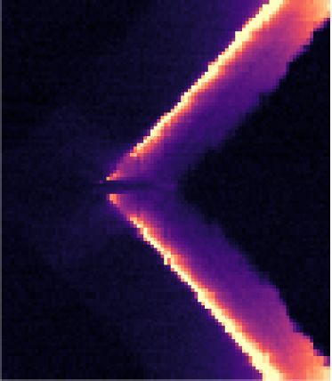
FEW-ELECTRON SINGLE AND DOUBLE QUANTUM. . .                                                       PRX QUANTUM 2, 010321 (2021)

drops abruptly when δ is increased beyond the borders of               exceeds the size of the bias window eVdc and we can thus
the bias triangle, where the system enters Coulomb block-              safely assume that transport involves only ground states;
ade, |eVdc | approximately 0.5 meV away from the baseline.             that is, the transport cycle is D↑(0,3) → T+ (1,3)
                                                                                                                          → S (0,4) →
The fact that the sharp resonances show a V shape in the                 (0,3)         (0,3)
                                                                       D↑ , where D↑ denotes the (0,3) charge state in a spin-
δ-B -plane is an indication that the (0,4) ground state is            up configuration. In that simple situation, where only three
a spin singlet: Indeed, if the (0,4) ground state were a               states are involved, the resonant current is expected to have
spin triplet, then the resonance between the (1,3) and (0,4)           a Lorentzian line shape [55],
triplet ground states should occur around the same value
of δ for all values of B . Furthermore, from the slope                                                    et2SF out
of the resonances we find |g ∗ | = 16.4, which is in good                      |Idc | =                                               ,   (1)
                                                                                         t2SF (2 + out / in ) + (out )2 /4 + δ 2
agreement with our earlier estimates.
   Extrapolating the two linear resonances to zero field
                                                                       where out and in denote the tunnel rates out of S (0,4) and
allows us to identify the gate voltage settings that corre-                    (1,3)
                                                                       into T+       , respectively. The coherent coupling between
spond to effective alignment of the energies of the (1,3) and             (1,3)
(0,4) charge states. From a high-resolution trace along B             T+ and S (0,4) involves a spin flip, and its strength is
very close to this point, shown in Fig. 6(b), we find a resid-          denoted by tSF . Assuming that out ∼ in and anticipat-
ual peak splitting of 46 mT, which corresponds to 44 μeV,              ing that tSF       out , we find Eq. (1) reduces to a peak with
close to zero detuning. This provides a measure for 2t,                a full width at half maximum of out and a peak value
where t is the coherent tunnel coupling strength between               of Imax = 4et2SF /2 out . Thus focusing on the sharp reso-
the (1,3) and (0,4) singlets [36].                                     nance in the data and disregarding the inelastic current tail,
   Next we focus on the current as a function of δ for fields           we fit the onset of each peak in the data in Fig. 6(c) to
|B | > 500 mT. At such large fields, the Zeeman splitting              a Lorentzian (adding a constant background offset as fit
                                                                       parameter). The result of one such fit, for B = 700 mT, is
                                                                       shown in Fig. 6(c), where the blue points represent the data
                                                                       and the green curve represents the fitted Lorentzian, yield-
(a)                                (b)
                    dc                                                 ing out = 25.5 μeV and Imax = 4.14 pA (which does not
                                                                       include the constant background). We repeat this procedure
                                                                       for all traces with |B | > 500 mT, which results after aver-
                                                                       aging in out = 31 ± 10 μeV and Imax = 4.00 ± 0.34 pA.
                                     dc

                                                                       Using these values, we find tSF = 0.36 ± 0.08 μeV.
                                                                          Finally, we investigate the underlying mechanism
                                                                                                                                   (1,3)
                                                                       responsible for the spin-flip tunnel coupling between T+
                                                                       and S (0,4) . We consider two common candidate mech-
                                                                       anisms: (i) Hyperfine interaction between the electron
(c)                                (d)                                 spins and the nuclear spin bath can result in a spin flip,
                                                                       after which the system can transition to (0,4) via a spin-
                                                                       conserving tunneling process.  √ This yields an effective cou-
                                                                       pling energy of tSF ∼ (1/ 2)t(K/|B |), where K is the
                                                                       typical magnitude of the effective nuclear fields acting on
   dc

                                                                       the electrons in the quantum dots. (ii) Spin-orbit coupling
                                                                       can induce a rotation of the spin state of electrons “dur-
                                                                       ing” tunneling between the quantum dots, resulting in a
                                                                                                         (1,3)
                                                                       coherent coupling√       between T+     and S (0,4) on the order
                                                                       of tSF ∼ (1/ 2)t(d/lSO ), where d is the distance between
FIG. 6. (a) Dependence of the magnitude of the leakage cur-            the quantum dots and lSO is the spin-orbit length along
rent |Idc | through the spin blockade involving the (1,3) to (0,4)     the interdot axis [56]. We see that mechanism (i) should
transition for strong interdot tunnel coupling on δ and B . A         result in a significant field dependence of tSF and thus
dip around zero external magnetic field is visible in the data.         Imax , whereas mechanism (ii) should produce a mostly
(b) High-resolution trace of |Idc | as a function of B around zero
detuning. (c) δ-dependent leakage current |Idc | at B = 700 mT
                                                                       field-independent tSF . In Fig. 6(d) we plot the fitted val-
(blue) and a Lorentzian fit to the onset of the peak (green) disre-     ues of Imax as a function of B , and we see that the peak
garding the inelastic current tail. (d) Peak current values Imax for   height is rather constant, suggesting that the spin-orbit
|B | > 500 mT, where the gray shaded area indicates the mag-          mechanism is dominating. Besides, for a hyperfine-driven
nitude of the error of each fit. Their field-independent height          spin-flip tunnel coupling the estimate of K ∼ 0.6 mT (see
suggests spin-orbit coupling as the main mechanism responsible         the next section) would produce tSF  20 neV for fields
for spin-flip tunneling rather than hyperfine coupling.                  |B | > 500 mT, which is far too small to explain the data.

                                                                010321-7
CHRISTOPHER MITTAG et al.                                                                   PRX QUANTUM 2, 010321 (2021)

 (a)                              (b)                 dc
                                                                      and δ, where δ is now measured along the dashed white line
                                                                      in Fig. 7(b). The strongest resonances appear in a V shape
             (1,3)        (2,3)           (1,3)      (2,3)            like in Fig. 6(a), mapping out where the (1,3) T+ ground
                                                                      state is resonant with the (2,2) singlet state. In addition
                                                                      to these resonances, we also observe a very narrow reso-
                                                                      nance at zero magnetic field, in contrast to the zero-field
           (1,2)         (2,2)                      (2,2)             dip we find in the strong-coupling regime. This peak in the
                                        (1,2)
                                                                      leakage current is caused by hyperfine coupling between
                                                                      the electron spins and the nuclear spins in the surround-
                                                                      ing crystal [36,58,59]. This coupling is now stronger than
 (c)                      dc            (d)          dc               the exchange effects caused by the interdot tunnel coupling
                                                                      and can thus efficiently mix all four (1,3) spin states at
                                                                      small magnetic fields, thereby lifting the blockade of the
                                                                      triplet states. From the enlargement of this resonance in
                                                                      Fig. 7(d), we find a full width at half maximum of approx-
                                                                      imately 0.6 mT; this indicates the typical magnitude of the
                                                                      random effective nuclear fields acting on the electron spins.
                                                                      This value is consistent with other values reported for
                                                                      InAs-based quantum dots [32,33,57] taking into account
                                                                      our comparatively large quantum dot volume and the large
FIG. 7. (a) Magnitude of the current |Idc | through the double        g factor in our system.
quantum dot system for weak interdot tunnel coupling and at a
finite bias of Vdc = +500 μV, close to the triple points involv-
ing the (2,2) to (1,3) transition. (b) Transitions from (1,3) to
(2,2) at Vdc = −500 μV are suppressed due to singlet-triplet spin                        V. CONCLUSION
blockade. For weak interdot tunnel coupling, a leakage current           In conclusion, we present the first realization of high-
is observed when the tunneling process is resonant. (c) Depen-
                                                                      quality gate-defined few-electron single and double quan-
dence of this leakage current on δ and B . A narrow resonance
around zero external magnetic field is observed. (d) Enlargement       tum dots in an InAs two-dimensional electron gas. We
of the dashed yellow box in (c) showing more clearly the zero-        obtain dc control over our quantum dots with similar preci-
field resonance arising from hyperfine coupling to the nuclear          sion as is common for GaAs- and Si-based quantum dots,
spins of the host crystal. The offset from B = 0 is due to residual   which have been around for decades. In the single quan-
magnetization in our experimental setup.                              tum dot, we observe a pronounced Kondo effect of the
                                                                      last electron and we characterize this effect consistently
Thus attributing tSF to spin-orbit coupling, we can estimate          with theory and previous experiments in other materi-
the spin-orbit length to be 8.6 ± 2.4 μm, assuming a spac-            als. Additionally, we perform excited state-spectroscopy,
ing of 200 nm between the quantum dot centers. This is                which allows us to determine a g factor of approximately
consistent with all the other estimates presented above.              16 and put a lower bound on the effective spin-orbit length
                                                                      in the system. In the double quantum dot we observe Pauli
                                                                      spin blockade, and analyze the leakage current for both
  D. Spin blockade for weak interdot tunnel coupling                  strong and weak interdot tunnel coupling to arrive at esti-
   On reducing the tunnel coupling between the two quan-              mates for the typical magnitude of the random hyperfine
tum dots, we enter a regime in which the spin blockade                fields on the quantum dots K ∼ 0.6 mT and the spin-orbit
manifests itself in a qualitatively different way [32,36,57].          length lSO ∼ 8 μm, which is almost 2 orders of magnitude
Figure 7(a) shows the current in the region close to the              longer than typically measured in InAs-based nanostruc-
boundary between the (2,2) and (1,3) charge regions at                tures. Together with the low effective electronic mass in
Vdc = 500 μV. The finite bias triangles in this forward                InAs, these results put InAs on the map as a competitive
direction show a pronounced baseline, corresponding to                base material for spin qubits.
resonant interdot tunneling, and quickly decaying current                The unusually large spin-orbit length we measure is
levels towards the tips of the triangles. The situation at            most likely due to the very symmetric design of our quan-
reverse bias in the spin blockade regime can be seen in               tum well in the out-of-plane direction, since any small
Fig. 7(b). Similarly to the forward direction, a pronounced           asymmetry in the potential is leveraged into strong spin-
baseline of the triangles is visible, but inside the triangles        orbit coupling by the large Rashba coefficient in InAs.
the current is now suppressed, which is qualitatively differ-          This combination of having weak spin-orbit coupling in
ent from the strong-coupling triangles shown in Fig. 5(c).            a material with a large Rashba coefficient could poten-
In Fig. 7(c) we plot the leakage current as a function of B          tially allow engineering of two-dimensional structures

                                                               010321-8
FEW-ELECTRON SINGLE AND DOUBLE QUANTUM. . .                                                  PRX QUANTUM 2, 010321 (2021)

where gate-induced electric fields generate strong spin-              [12] N. W. Hendrickx, W. I. L. Lawrie, M. Russ, F. van Riggelen,
orbit interaction locally in space and/or time.                           S. L. de Snoo, R. N. Schouten, A. Sammak, G. Scappucci,
                                                                          and M. Veldhorst, arXiv:2009.04268.
                 ACKNOWLEDGMENTS                                     [13] F. A. Zwanenburg, A. S. Dzurak, A. Morello, M. Y. Sim-
                                                                          mons, L. C. L. Hollenberg, G. Klimeck, S. Rogge, S.
   The authors acknowledge the support of the ETH FIRST                   N. Coppersmith, and M. A. Eriksson, Silicon quantum
laboratory and the financial support of the Swiss Sci-                     electronics, Rev. Mod. Phys. 85, 961 (2013).
ence Foundation (Schweizerischer Nationalfonds, NCCR                 [14] F. Nichele, H. J. Suominen, M. Kjaergaard, C. M. Mar-
QSIT). The work at Purdue University was funded by                        cus, E. Sajadi, J. A. Folk, F. Qu, A. J. A. Beukman, F. K.
                                                                          d. Vries, J. v. Veen, S. Nadj-Perge, L. P. Kouwenhoven,
Microsoft Quantum. J.D. acknowledges support through
                                                                          B.-M. Nguyen, A. A. Kiselev, W. Yi, M. Sokolich, M. J.
FRIPRO project 274853, which is funded by the Research                    Manfra, E. M. Spanton, and K. A. Moler, Edge transport in
Council of Norway.                                                        the trivial phase of InAs/GaSb, New. J. Phys. 18, 083005
                                                                          (2016).
                                                                     [15] B.-M. Nguyen, A. A. Kiselev, R. Noah, W. Yi, F. Qu, A. J.
                                                                          Beukman, F. K. de Vries, J. van Veen, S. Nadj-Perge, L. P.
 [1] D. Loss and D. P. DiVincenzo, Quantum computation with               Kouwenhoven, M. Kjaergaard, H. J. Suominen, F. Nichele,
     quantum dots, Phys. Rev. A 57, 120 (1998).                           C. M. Marcus, M. J. Manfra, and M. Sokolich, Decoupling
 [2] A. V. Khaetskii, D. Loss, and L. I. Glazman, Electron                Edge Versus Bulk Conductance in the Trivial Regime of
     Spin Decoherence in Quantum Dots due to Interaction with             an InAs/GaSb Double Quantum Well Using Corbino Ring
     Nuclei, Phys. Rev. Lett. 88, 186802 (2002).                          Geometry, Phys. Rev. Lett. 117, 077701 (2016).
 [3] F. H. L. Koppens, C. Buizert, K.-J. Tielrooij, I. T. Vink,      [16] S. Mueller, C. Mittag, T. Tschirky, C. Charpentier, W.
     K. C. Nowack, T. Meunier, L. P. Kouwenhoven, and L. M.               Wegscheider, K. Ensslin, and T. Ihn, Edge transport in InAs
     K. Vandersypen, Driven coherent oscillations of a single             and InAs/GaSb quantum wells, Phys. Rev. B 96, 075406
     electron spin in a quantum dot, Nature 442, 766 (2006).              (2017).
 [4] J. R. Petta, A. C. Johnson, J. M. Taylor, E. A. Laird,          [17] C. Mittag, M. Karalic, S. Mueller, T. Tschirky, W.
     A. Yacoby, M. D. Lukin, C. M. Marcus, M. P. Hanson, and              Wegscheider, O. Nazarenko, M. V. Kovalenko, T. Ihn,
     A. C. Gossard, Coherent manipulation of coupled electron             and K. Ensslin, Passivation of edge states in etched InAs
     spins in semiconductor quantum dots, Science 309, 2180               sidewalls, Appl. Phys. Lett. 111, 082101 (2017).
     (2005).                                                         [18] R. Winkler, Spin-Orbit Coupling Effects in Two-
 [5] J. Medford, J. Beil, J. M. Taylor, E. I. Rashba, H. Lu, A. C.        Dimensional Electron and Hole Systems, Springer Tracts
     Gossard, and C. M. Marcus, Quantum-Dot-Based Resonant                in Modern Physics, Vol. 191, Springer Berlin Heidelberg,
     Exchange Qubit, Phys. Rev. Lett. 111, 050501 (2013).                 Berlin, Heidelberg, 2003.
 [6] J. Yoneda, K. Takeda, T. Otsuka, T. Nakajima, M. R. Del-        [19] D. Grundler, Large Rashba Splitting in InAs Quantum
     becq, G. Allison, T. Honda, T. Kodera, S. Oda, Y. Hoshi,             Wells due to Electron Wave Function Penetration Into the
     N. Usami, K. M. Itoh, and S. Tarucha, A quantum-dot spin             Barrier Layers, Phys. Rev. Lett. 84, 6074 (2000).
     qubit with coherence limited by charge noise and fidelity        [20] A. Y. Kitaev, Unpaired majorana fermions in quantum
     higher than 99.9%, Nat. Nanotechnol. 13, 102 (2018)..                wires, Physics-Uspekhi 44, 131 (2001).
     1708.01454                                                      [21] J. D. Sau, R. M. Lutchyn, S. Tewari, and S. Das Sarma,
 [7] W. Huang, C. H. Yang, K. W. Chan, T. Tanttu, B. Hensen,              Generic new Platform for Topological Quantum Compu-
     R. C. C. Leon, M. A. Fogarty, J. C. C. Hwang, F. E. Hud-             tation Using Semiconductor Heterostructures, Phys. Rev.
     son, K. M. Itoh, A. Morello, A. Laucht, and A. S. Dzurak,            Lett. 104, 040502 (2010).
     Fidelity benchmarks for two-qubit gates in silicon, Nature      [22] R. M. Lutchyn, J. D. Sau, and S. Das Sarma, Majo-
     569, 532 (2019).                                                     rana Fermions and a Topological Phase Transition
 [8] L. Petit, H. G. J. Eenink, M. Russ, W. I. L. Lawrie, N. W.           in Semiconductor-Superconductor Heterostructures, Phys.
     Hendrickx, S. G. J. Philips, J. S. Clarke, L. M. K. Vander-          Rev. Lett. 105, 077001 (2010).
     sypen, and M. Veldhorst, Universal quantum logic in hot         [23] Y. Oreg, G. Refael, and F. von Oppen, Helical Liquids and
     silicon qubits, Nature 580, 355 (2020).                              Majorana Bound States in Quantum Wires, Phys. Rev. Lett.
 [9] C. H. Yang, R. C. Leon, J. C. Hwang, A. Saraiva, T. Tanttu,          105, 177002 (2010).
     W. Huang, J. Camirand Lemyre, K. W. Chan, K. Y. Tan,            [24] D. A. Ivanov, Non-Abelian Statistics of Half-Quantum Vor-
     F. E. Hudson, K. M. Itoh, A. Morello, M. Pioro-Ladrière,             tices in p-Wave Superconductors, Phys. Rev. Lett. 86, 268
     A. Laucht, and A. S. Dzurak, Operation of a silicon quan-            (2001).
     tum processor unit cell above one kelvin, Nature 580, 350       [25] C. Nayak, S. H. Simon, A. Stern, M. H. Freedman,
     (2020).                                                              and S. Das Sarma, Non-abelian anyons and topologi-
[10] H. Watzinger, J. Kukučka, L. Vukušić, F. Gao, T. Wang,             cal quantum computation, Rev. Mod. Phys. 80, 1083
     F. Schäffler, J.-J. Zhang, and G. Katsaros, A germa-                   (2008).
     nium hole spin qubit, Nat. Commun. 9, 3902 (2018).              [26] V. Mourik, K. Zuo, S. M. Frolov, S. R. Plissard, E.
     http://www.nature.com/articles/s41467-018-06418-4                    P. A. M. Bakkers, and L. P. Kouwenhoven, Signa-
[11] F. N. M. Froning, L. C. Camenzind, O. A. H. van der Molen,           tures of majorana fermions in hybrid superconductor-
     A. Li, E. P. A. M. Bakkers, D. M. Zumbühl, and F. R.                 semiconductor nanowire devices, Science 336, 1003
     Braakman, arXiv:2006.11175.                                          (2012).

                                                              010321-9
CHRISTOPHER MITTAG et al.                                                                      PRX QUANTUM 2, 010321 (2021)

[27] M. T. Deng, S. Vaitiekėnas, E. B. Hansen, J. Danon,                  using a quantum point contact, Appl. Phys. Lett. 85, 4394
     M. Leijnse, K. Flensberg, J. Nygård, P. Krogstrup, and                (2004).
     C. M. Marcus, Majorana bound state in a coupled                [42]   C. Ellenberger, T. Ihn, C. Yannouleas, U. Landman, K.
     quantum-dot hybrid-nanowire system, Science 354, 1557                 Ensslin, D. Driscoll, and A. C. Gossard, Excitation Spec-
     (2016).                                                               trum of Two Correlated Electrons in a Lateral Quantum
[28] H. Zhang, C.-X. Liu, S. Gazibegovic, D. Xu, J. A. Logan,              Dot with Negligible Zeeman Splitting, Phys. Rev. Lett. 96,
     N. V. Loo, J. D. S. Bommer, M. W. A. D. Moor, D. Car,                 126806 (2006).
     R. L. M. Op, P. J. V. Veldhoven, S. Koelling, and M. A.        [43]   J. Konopka, Conduction electron spin resonance in InAs,
     Verheijen, Quantized majorana conductance, Nature 556,                Phys. Lett. A 26, 29 (1967).
     74 (2018). http://www.nature.com/articles/nature26142          [44]   C. R. Pidgeon, D. L. Mitchell, and R. N. Brown, Interband
[29] M. Hell, M. Leijnse, and K. Flensberg, Two-Dimensional                magnetoabsorption in InAs and InSb, Phys. Rev. 154, 737
     Platform for Networks of Majorana Bound States, Phys.                 (1967).
     Rev. Lett. 118, 107701 (2017).                                 [45]   The fact that resonance S changes sign when it crosses
[30] C. Fasth, A. Fuhrer, L. Samuelson, V. N. Golovach, and                resonance T signals that the actual rates corresponding to
     D. Loss, Direct Measurement of the Spin-Orbit Interac-                all transitions contributing to electron transport are signifi-
     tion in a Two-Electron InAs Nanowire Quantum Dot, Phys.               cantly different, most likely due to differences in the orbital
     Rev. Lett. 98, 266801 (2007).                                         structure of the states involved and/or asymmetric coupling
[31] A. Pfund, I. Shorubalko, K. Ensslin, and R. Leturcq, Spin-            to the source and drain leads.
     state mixing in InAs double quantum dots, Phys. Rev. B 76,     [46]   J. Nitta, T. Akazaki, H. Takayanagi, and T. Enoki,
     161308 (2007).                                                        Gate Control of Spin-Orbit Interaction in an Inverted
[32] S. Nadj-Perge, S. M. Frolov, J. W. W. van Tilburg, J. Danon,          In0.53 Ga0.47 As/In0.52 Al0.48 As Heterostructure, Phys. Rev.
     Y. V. Nazarov, R. Algra, E. P. A. M. Bakkers, and L. P.               Lett. 78, 1335 (1997).
     Kouwenhoven, Disentangling the effects of spin-orbit and        [47]   G. Dresselhaus, Spin-orbit coupling effects in zinc blende
     hyperfine interactions on spin blockade, Phys. Rev. B 81,              structures, Phys. Rev. 100, 580 (1955).
     201305 (2010).                                                 [48]   S. Brosig, K. Ensslin, R. J. Warburton, C. Nguyen, B.
[33] S. Nadj-Perge, S. M. Frolov, E. P. a. M. Bakkers, and                 Brar, M. Thomas, and H. Kroemer, Zero-field spin split-
     L. P. Kouwenhoven, Spin-orbit qubit in a semiconductor                ting in InAs-AlSb quantum wells revisited, Phys. Rev. B
     nanowire, Nature 468, 1084 (2010).                                    60, R13989 (1999).
[34] C. Mittag, M. Karalic, Z. Lei, T. Tschirky, W. Wegscheider,    [49]   D. Goldhaber-Gordon, H. Shtrikman, D. Mahalu, D.
     T. Ihn, and K. Ensslin, Edgeless and purely gate-defined               Abusch-Magder, U. Meirav, and M. A. Kastner, Kondo
     nanostructures in InAs quantum wells, Appl. Phys. Lett.               effect in a single-electron transistor, Nature 391, 156
     113, 262103 (2018).                                                   (1998).
[35] In experiments searching for possible beating patterns in      [50]   S. M. Cronenwett, T. H. Oosterkamp, and L. P. Kouwen-
     Shubnikov–de Haas oscillations signaling spin-orbit split             hoven, A tunable kondo effect in quantum dots, Science
     bands, a negative result was reported many years ago for              281, 540 (1998).
     samples quite similar to those investigated in our present     [51]   A. V. Kretinin, H. Shtrikman, D. Goldhaber-Gordon,
     work [48].                                                            M. Hanl, A. Weichselbaum, J. von Delft, T. Costi, and
[36] F. H. L. Koppens, J. A. Folk, J. M. Elzerman, R. Hanson,              D. Mahalu, Spin- 12 kondo effect in an InAs nanowire quan-
     L. H. W. v. Beveren, I. T. Vink, H. P. Tranitz, W. Wegschei-          tum dot: Unitary limit, conductance scaling, and zeeman
     der, L. P. Kouwenhoven, and L. M. K. Vandersypen, Con-                splitting, Phys. Rev. B 84, 245316 (2011).
     trol and detection of singlet-triplet mixing in a random       [52]   K. Ono, D. G. Austing, Y. Tokura, and S. Tarucha, Current
     nuclear field, Science 309, 1346 (2005).                               rectification by pauli exclusion in a weakly coupled double
[37] O. N. Jouravlev and Y. V. Nazarov, Electron Trans-                    quantum dot system, Science 297, 1313 (2002).
     port in a Double Quantum Dot Governed by a Nuclear             [53]   In principle, due to intradot Coulomb interaction, the four-
     Magnetic Field, Phys. Rev. Lett. 96, 176804 (2006).                   electron ground state in a quantum dot can also be a spin
     http://link.aps.org/abstract/PRL/v96/e176804                          triplet, depending on the shape and size of the quantum dot.
[38] R. Hanson, L. P. Kouwenhoven, J. R. Petta, S. Tarucha, and            However, our field-dependent measurements of the current
     L. M. K. Vandersypen, Spins in few-electron quantum dots,             in the spin blockade regime suggest that the (0, 4) ground
     Rev. Mod. Phys. 79, 1217 (2007).                                      state is a singlet; see Sec. IV C.
[39] C. Thomas, A. T. Hatke, A. Tuaz, R. Kallaher, T. Wu,           [54]   A. C. Johnson, J. R. Petta, C. M. Marcus, M. P. Hanson,
     T. Wang, R. E. Diaz, G. C. Gardner, M. A. Capano, and M.              and A. C. Gossard, Singlet-triplet spin blockade and charge
     J. Manfra, High-mobility InAs 2DEGs on GaSb substrates:               sensing in a few-electron double quantum dot, Phys. Rev.
     A platform for mesoscopic quantum transport, Phys. Rev.               B 72, 165308 (2005).
     Mater. 2, 104602 (2018).                                       [55]   T. H. Stoof and Y. V. Nazarov, Time-dependent resonant
[40] R. Schleser, E. Ruh, T. Ihn, K. Ensslin, D. C. Driscoll,              tunneling via two discrete states, Phys. Rev. B 53, 1050
     and A. C. Gossard, Time-resolved detection of individual              (1996).
     electrons in a quantum dot, Appl. Phys. Lett. 85, 2005         [56]   J. Danon, Spin-flip phonon-mediated charge relaxation
     (2004).                                                               in double quantum dots, Phys. Rev. B 88, 075306
[41] L. M. K. Vandersypen, J. M. Elzerman, R. N. Schouten, L.              (2013).
     H. Willems van Beveren, R. Hanson, and L. P. Kouwen-           [57]   A. Pfund, I. Shorubalko, K. Ensslin, and R. Leturcq,
     hoven, Real-time detection of single-electron tunneling               Suppression of Spin Relaxation in an InAs Nanowire

                                                             010321-10
FEW-ELECTRON SINGLE AND DOUBLE QUANTUM. . . PRX QUANTUM 2, 010321 (2021)
Double Quantum Dot, Phys. Rev. Lett. 99, 036801 [59] A. C. Johnson, J. R. Petta, J. M. Taylor, A. Yacoby,
(2007). M. D. Lukin, C. M. Marcus, M. P. Hanson, and
[58] K. Ono and S. Tarucha, Nuclear-Spin-Induced Oscillatory A. C. Gossard, Triplet–singlet spin relaxation via nuclei
Current in Spin-Blockaded Quantum Dots, Phys. Rev. Lett. in a double quantum dot, Nature 435, 925
92, 256803 (2004). (2005).
010321-11You can also read