Transparent Gatable Superconducting Shadow Junctions
←
→
Page content transcription
If your browser does not render page correctly, please read the page content below

Transparent Gatable Superconducting Shadow Junctions

                                                     Sabbir A. Khan,1, 2, ∗ Charalampos Lampadaris,1, 2 Ajuan Cui,1, 2 Lukas Stampfer,2 Yu Liu,1, 2 S. J. Pauka,3 Martin
                                                      E. Cachaza,1, 2 Elisabetta M. Fiordaliso,4 Jung-Hyun Kang,1, 2 Svetlana Korneychuk,5 Timo Mutas,2 Joachim E.
                                                         Sestoft,2 Filip Krizek,2 Rawa Tanta,1, 2 M. C. Cassidy,3 Thomas S. Jespersen,2 and Peter Krogstrup1, 2, †
                                                                              1
                                                                              Microsoft Quantum Materials Lab Copenhagen, 2800 Lyngby, Denmark
                                                                                        2
                                                                                          Center for Quantum Devices, Niels Bohr Institute,
                                                                                      University of Copenhagen, 2100 Copenhagen, Denmark
                                                                      3
                                                                        Microsoft Quantum Sydney, The University of Sydney, Sydney, NSW 2006, Australia
                                                                         4
                                                                           DTU Nanolab, Technical University of Denmark, 2800 Kgs. Lyngby, Denmark
                                                            5
                                                              QuTech and Kavli Institute of Nanoscience, Delft University of Technology, 2600 GA Delft, The Netherlands
arXiv:2003.04487v1 [cond-mat.mtrl-sci] 10 Mar 2020

                                                                                                      (Dated: March 11, 2020)
                                                                    Gate tunable junctions are key elements in quantum devices based on hybrid semiconductor-
                                                                  superconductor materials. They serve multiple purposes ranging from tunnel spectroscopy probes
                                                                  to voltage-controlled qubit operations in gatemon and topological qubits. Common to all is that
                                                                  junction transparency plays a critical role. In this study, we grow single crystalline InAs, InSb and
                                                                  InAs1−x Sbx nanowires with epitaxial superconductors and in-situ shadowed junctions in a single-
                                                                  step molecular beam epitaxy process. We investigate correlations between fabrication parameters,
                                                                  junction morphologies, and electronic transport properties of the junctions and show that the ex-
                                                                  amined in-situ shadowed junctions are of significantly higher quality than the etched junctions. By
                                                                  varying the edge sharpness of the shadow junctions we show that the sharpest edges yield the highest
                                                                  junction transparency for all three examined semiconductors. Further, critical supercurrent mea-
                                                                  surements reveal an extraordinarily high IC RN , close to the KO−2 limit. This study demonstrates
                                                                  a promising engineering path towards reliable gate-tunable superconducting qubits.

                                                        Josephson junctions (JJs) are critical circuit ele-           conductance peaks expected from MBS [25–27]. Avoiding
                                                     ments superconducting quantum computing. Gate tun-               such misinterpretations is certainly desirable and a cru-
                                                     able junctions based on proximitized semiconducting              cial reason to aim for disorder free junctions. Junctions
                                                     segments in hybrid semiconductor (SE)-superconductor             in spectroscopy devices have been demonstrated with a
                                                     (SU) materials are an interesting class of junctions with        top-down etching process [21, 28, 29], while a more recent
                                                     potential as JJ elements in transmons qubits [1, 2] as           alternative approach has been using an in-situ shadow
                                                     well as critical operators in topological qubits [3]. Simi-      method [30–32]. The in-situ process leaves the SE sur-
                                                     lar to all semiconducting circuit elements, they are highly      face as it was grown, which seems to be an ideal fabri-
                                                     susceptible to disorder and require dedicated optimiza-          cation approach for gate tunable junctions even though
                                                     tion for development towards high fidelity gate opera-           a detailed analysis of the junction formation along with
                                                     tions. In the case of topological quantum computing,             correlations between fabrication and junction quality are
                                                     achieving disorder free junctions is desirable on several        still missing.
                                                     levels. Coupling a one-dimensional semiconductor with
                                                     strong spin-orbit interaction and large Landé-g factor to           In this work, we study the synthesis of stacking-fault
                                                     a conventional s-wave superconductor has the fundamen-           free InAs, InSb and InAs1−x Sbx NWs with epitaxially
                                                     tal ingredients to generate topologically protected Majo-        grown superconductors containing shadowed junctions in
                                                     rana bound states (MBS) [4–8]. If the material fulfills          single-step growth process using molecular beam epitaxy
                                                     the set of requirements, MBS are expected to tolerate            (MBE). To obtain shadowed junctions at predefined po-
                                                     local perturbations and therefore makes it a promising           sitions we use (111)B faceted trenches on InAs (100)
                                                     candidate for scalable quantum computing [3, 9, 10]. In          substrates for NWs growth [31, 33]. This method pro-
                                                     recent years, there has been significant progress in the de-     vides freedom for controlled positioning of the shadow
                                                     velopment of epitaxially grown SE-SU hybrid materials            junctions due to the specified NW growth directions.
                                                     to fulfill these requirements [11–15]. Even though elec-         We study the formation of junctions as a function of
                                                     tronic tunnel spectroscopy has yielded results that have         the inter-wire distance between the shadowing NW and
                                                     been interpreted as signatures of MBS [16–24], direct ev-        the junction NW. We also analyze the junction profile,
                                                     idence for topologically protected MBS is still missing.         which directly depends on the flux distribution from the
                                                     Complications in the process of verifying the MBS with           source and geometry of the shadowing. Further with
                                                     tunnel spectroscopy relate not only to the hybrid SE-SU          different superconductors we investigate the influence of
                                                     nanowire (NW) segments but also the tunnel junctions             growth kinetics on the junction sharpness. Developing
                                                     which may contain random disorders that may give rise            a pre-growth substrate fabrication process including op-
                                                     to local Andreev bound states that mimic the zero-bias           timized growth and shadow conditions, we demonstrate
                                                                                                                      high junction transparency with reproducible quantized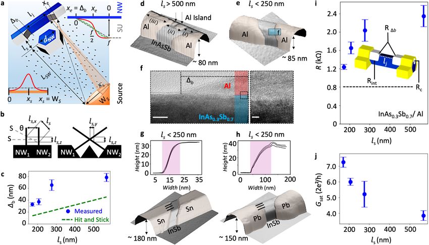
2

FIG. 1. Semiconductor-superconductor nanowires with shadow junctions. a, Scanning electron micrograph (SEM,
30◦ tilted) of Au-assisted InAs NW array grown on the pre-processed "V" groove (111)B faceted InAs trenches. b, V/III ratio
as a function of InAs NW growth temperature (TG ). The plot is divided into six regions (A-F), and NW growth outcome
(yield, morphology, etc.) of each region is investigated. Region "D" (TG ∼ 401-415◦ C with V/III ratio ∼ 9-10.5) shows the
highest yield and uniform InAs NW growth (dark green circles). c, SEM image of InSb NWs grown from InAs stems. d,
Schematic with crystal orientation of the hybrid NWs. Dashed arrow shows the superconductor deposition direction. In the
right, schematic of superconductor deposition geometry on the NW with respect to the beam flux direction and the NW growth
axis. Here, α is the angle between these two vectors to calculate effective flux (f 0 ) on the NW facet. e, Schematic of 3-facets
and 2-facets superconductor on the NWs. The table provides the beam angle requirements in the case when φ=0, for 2-facets
and 3-facets superconductor coverage. f, Tilted SEM image of InSb NWs with epitaxially grown Al. g, SEM image of InSb/Sn
NWs with junctions. h, SEM image of InSb/Pb NW with junction. Orange arrows indicate the shadowed junctions. Dashed
arrows indicate the direction of superconductor deposition. Scale bars for (a), (c), (f), (g) and (h) are 1 μm. Scale bar for (f)
inset is 100 nm.

transport. Correlations between the structural and elec-             The NW substrates are fabricated using electron beam
tronic properties of the junctions are done by statistical        lithography (EBL) and wet-etching process to form
characterization of the junction morphology and trans-            (111)B facets in planar InAs (100) substrates, where the
port properties of junction NWs from selected positions           Au catalysts are positioned with a subsequent EBL pro-
on the growth substrate. We compare in-situ shadowed              cess. As opposed to earlier works [31, 33], we do not use
and etched junctions on statistical ensembles of NW de-           any masks to confine the Au particles, which significantly
vices as well as on the same InAs1−x Sbx /Al NWs and              reduces the pre-processing efforts and minimizes contam-
confirm the superior electrical quality for the shadowed          ination during fabrication. This makes the process suit-
junctions. Finally, measurements at mK temperatures               able for exploring different material combinations with
show an IC RN products over 7 samples close to the KO−2           high throughput. Figure 1a shows an SEM image of
and KO−1 limit. Voltage bias measurements reveal the              InAs NWs grown from (111)B trenches. However, the
size of the induced superconducting gap, as well as a             NW growths on the trenches require careful optimiza-
phase coherence of at least 5 times of the junction length.       tion of the growth conditions. We find out that As4
3

beam flux is necessary to enhance the initial NW growth       only vary semiconductor composition but also the super-
rate to escape the competition with planar growth in the      conducting materials, providing a versatile platform for
trenches. In Fig. 1b we show a map of InAs NW growth          exploring wide range of hybrid material combinations.
yield, which resembles the design of growth parameter         Two promising superconductor alternatives to Al are Sn
optimization. Dark to light green color represents high       and Pb, which both have higher Tc (for bulk it is around
(> 90%) to low yield (< 50%) growth of NWs and gray           3.7 K for Sn and 7.2 K for Pb, compared to 1.2 K for
resembles no growth. To help tuning in the right growth       Al). As these superconducting materials are challenging
parameter space we distinguish between six growth pa-         to etch selectively without damaging the semiconducting
rameter regions which are discussed in supplementary in-      NW segments, the shadowing method may be critical for
formation S2. The growth temperature window in region         the realization of high-quality junctions. In Fig. 1g and
"D" with V/III ratio ∼ 9-10.5 provides the highest yield      Fig. 1h we show Sn and Pb phases grown on InSb and
and uniform morphology of the NWs, while outside of           InAs1−x Sbx NWs, respectively. After the semiconductor
this region the growth either has uneven yield issue or       NW growth, the Sn and Pb are grown on liquid nitrogen
non-uniform NWs. We mostly grow in the lower side             cooled stage in a UHV chamber connected to the MBE.
of the growth temperature window in region "D", as we         The shadowing and formation of the junction details will
get pure wurtzite (WZ) crystal structure at lower tem-        be discussed below.
peratures, verified by TEM analysis (see supplementary           Having growth conditions for InAs and InSb NWs on
information S3). Confirming previous reports [34], we         the trenches, the As and Sb fluxes can be tuned to grow
are also not able to grow InSb NWs directly from the          InAs1−x Sbx /Al NWs [12] as shown in Fig. 2a. Similar
InAs substrate. It is speculated that the Au-alloy forms      to InSb NWs, we initiate the InAs1−x Sbx NW growth
a small contact angle to the substrate when Sb is present,    with an InAs stem (using the recipe from 1b, region
which prevents initiation of NW growth [34]. However,         "D"). The InAs stem is not visible in Fig. 2a due to
once the InAs NW stem is formed it is possible to switch      the over-growth on the substrate. To enhance spin-orbit
into InSb NW growth. With optimized growth condi-             interaction [36] while maintaining an efficient field effect
tions (in region "D"), we achieve high yield InSb NWs         response by keeping the carrier density low [12, 37] we
across the substrate as shown in Fig. 1c.                     aim at for Sb composition around x=0.7 (nominal Sb/As
   Figure 1d shows the schematic of the NWs with shadow       flux ratio of 0.8). The composition of the InAs0.3 Sb0.7 /Al
junction as grown on the substrate. On the right, the         NWs are measured applying Vegard’s law [38] for the lat-
hemisphere diagram shows the coordinates use to de-           tice parameter in ternary alloys (see supplementary in-
scribe the superconductor beam flux direction with re-        formation S6 for STEM-EDX analysis).
spect to NWs. Depending on the angle of the incom-               These InAs0.3 Sb0.7 /Al NWs are used to compare the
ing flux and orientation of the NW facets, the super-         field-effect response of etched and shadowed junctions as
conductor can be grown on selected facets. The table          shown in Fig. 2b and 2c. The challenge for etched junc-
in Fig. 1e contains information of beam flux angles re-       tions is to find conditions that selectively etch Al while
quired for 2-facet and 3-facet superconductor coverage on     leaving the semiconductor unharmed. As for instance,
[11̄0]ZB /[112̄0]WZ and [112̄]ZB /[11̄00]WZ oriented NWs.     we have not been able to find selective etch conditions
The amount of superconductor that is grown on each            for Al on InSb. For InAs0.3 Sb0.7 and InAs NWs, we use
facet (for a given growth time) is proportional to the ef-    etch conditions which were optimized in previous studies
fective beam flux (f 0 ) on the selected facet. Here f 0 is   and apparently leave the semiconductor intact [12, 39]
defined as the flux impinging on the mid-facet facing the     (see supplementary information S7 for details). Because
source during 3-facet deposition (see Fig. 1e). If we con-    the electron transport characteristics vary from device
sider 2-facet depositions then both facets receive equal      to device, we need statistics for comparing quality mea-
amounts of material,
                   √
                        as an instance, for φ=0 and θ=35◦ ,   sures. For this purpose, we compare 41 back-gated de-
                     3 0
f[1̄01] = f[011] = 2 f . For 3-facet depositions, the facet   vices, 31 with shadowed and 10 with etched junctions,
facing towards the beam receives f 0 , while the adjacent     see Fig. 2b. For etched junctions, 7 out of the 10 devices
facets get f 0 /2. An SEM image of InSb/Al NWs with           are first measured at 20 mK out of which 6 pinch-off
in-situ junctions are demonstrated in Fig. 1f, where the      with a threshold voltage of −3 ± 1 V, a mean satura-
inset shows a ∼ 100 nm long junction. Because the NW          tion conductance of 1.6 ± 0.2 2e2 /h and the field-effect
positions are controlled, it is possible to design multiple   mobility µFE ≈ 1900 ± 600 cm2 /Vs (highest µFE ≈ 4400
junctions in a single NW, see supplementary information       cm2 /Vs). As a comparison, we measure 9 shadowed de-
S5 for different junction schemes.                            vices under identical conditions where 4 devices pinch-off
   Synthesis of hybrid InSb/Sn NWs with junctions has         with a mean threshold voltage of −36.0 ± 2.5 V and rest
recently been reported [35], showing a route for deposi-      haven’t pinched-off within the applied gate voltage. The
tion of alternative superconductors on bare semiconduc-       mean saturation conductance of all shadowed devices is
tor NW facets. Due to the simplicity of the single UHV-       9 ± 1 2e2 /h.
step process demonstrated in this work, it is easy to not        For a higher throughput we turn to measurement at 2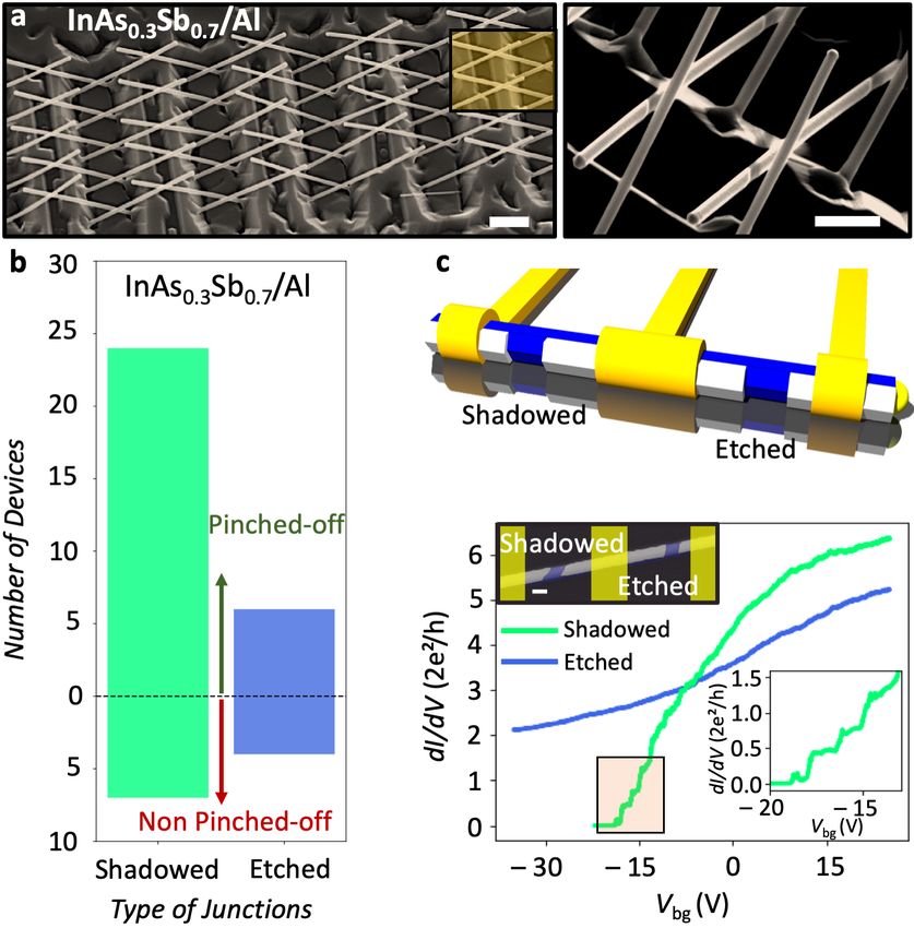
4

K and measure 22 devices with shadowed junctions where
20 devices pinch-off with a mean µFE ≈ 17000 ± 400
cm2 /Vs (highest µFE ≈ 35000 cm2 /Vs). The mean
threshold voltage and saturation conductance of these
devices are −13±2 V and 5.1±0.5 2e2 /h respectively. In
comparison, three etched junctions are characterized at
2 K showing a low gate response and no pinch-off within
the voltage limits of the system and with mean satura-
tion conductance of 4.1±0.7 2e2 /h. In short, according to
the statistics presented above, shadow junctions exhibit a
significantly higher conductance and mobility compared
to the etched junctions.
   As an additional comparison we fabricate 11 devices
with comparable sized etched and shadowed junctions
in the same InAs0.3 Sb0.7 /Al NW (shown in Figure 2c).
Among them, only three devices are functional on both
sides, where the electrical measurement of one of these
devices is demonstrated in Fig. 2c. Despite the almost
identical appearance of the etched and shadowed junc-
tions in these devices, a radical difference is observed
in the transport properties. Here the shadow junction
pinched off with clear quantized conductance plateaus
around magnetic field, B > 4 T, while the etched junction
is not pinched-off within the available voltage range. Sim-      FIG. 2. Gate response statistics of shadowed and
ilar differences are observed for the other two devices pre-     etched junctions in InAs0.3 Sb0.7 /Al nanowires. a, SEM
sented in supplementary information S8. We note that             (30◦ tilted) of InAs0.3 Sb0.7 /Al NW array (scale bar is 1μm).
                                                                 The highlighted section shows double shadowed junctions on
there can be many reasons for disorders associated with
                                                                 the NWs (scale bar is 500 nm). b, Pinch-off statistics of
etching such as undercut during wet etching, increased           the back-gated devices with shadowed (green) and etched
SE surface roughness, impurities left from etchant and           (blue) junctions. The y-axis contains the number of devices
leftovers from the etched metal (see supplementary infor-        where the upper side of the dotted line shows devices that
mation S7). There are most likely ways to improve etch           are pinched-off and lower side shows devices that are not
recipes, however, unless the etch actively provides protec-      pinched-off. c, Schematic of the test device with comparable
tion, it is reasonable to assume that optimized shadowed         size shadowed and etched junctions in a single NW. Below,
                                                                 electrical measurements of the test device where conductance
junctions will generally be of the highest possible quality.
                                                                 is shown as a function of gate voltage for shadowed (green)
Additionally, besides obtaining higher quality junctions,        and etched (blue) junctions. The shadowed junction shows
shadowed junctions allow flexibility in the choice of ma-        quantized plateaus as highlighted with inset. Applied mag-
terial combinations, where selective etching may be in-          netic field, B=6 T in both cases. SEM image of the exact
feasible. Based on this and the above results, we choose         NW is shown inset with a scale bar of 100 nm.
to solely focus on shadow junctions for all material com-
binations.
   The influence of the junction edge morphology on the          a cutoff area up to WS − LSW  ls xe of the source opening
junction transparency is studied by comparing devices            (cutoff determined by xe ) as shown in Fig 3a. Thus,
with varying edge sharpness. The edge sharpness is var-          a point in the transition region xe sees a fraction of the
ied by changing inter-wire distance, ls , between the shad-      source from where the effective impinging flux originates.
owing and the shadowed NW. The reason is sketched in             If the outgoing flux distribution within the source open-
Fig 3a, where the transition region going from a fully           ing is uniform, it can be shown that the effective flux
shadowed region to a fully unblocked region (with nom-           in the transition region is given by: f 0 (xe ) = πf [ π2 − Xe
                                           W S ls                p
                                                                    1 − Xe2 − arcsin Xe ] where, Xe = 2L
                                                                                                       ls WS xe − 1. Such an
                                                                                                          SW
inal beam-flux f ) is given by ∆b =               . Here LSW
                                           LSW                   outgoing flux distribution originating from an uniform
is the "source to wire" distance and WS is the width of
                                                                 circular source opening would give a flux distribution in
the source opening. The effective flux in the transition
                                                                 the transition region as shown in the dashed green line
region f 0 (xe ) as a function of coordinate 0 < xe < ∆b is
                                                                 in the inset of Fig 3a, while an uniform beam estimated
directly related to the flux distribution across the source
                        R WS − LSW                               from a 2D model (or from a hypothetical squared source
                                ls xe
opening as f 0 (xe ) ∝ 0              fsource dr. Here fsource   opening) would provide a linearly increasing flux distri-
is the beam-flux originating from a point source within          bution as a reasonable approximation (as shown with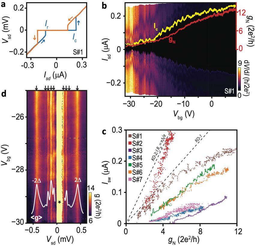
5

FIG. 3. Edge profile effect on the junction performance. a, Schematic of the SE-SU junction formation and the edge
profile. The broadening (∆b ) and profile of the junction edge can be determined by the flux distribution in the transition
region, inter-wire distances (ls ), source to wire distance (LSW ) and effective width of the source (Ws ). The junction length (`j )
depends on the size of the ∆b and the diameter of the shadowing NW (dN W ). (diagram is not drawn to scale). b, Geometry
for determining the shadow position. c, ∆b as a function of ls . Blue dots are measured ∆b for Al junctions on InAs0.3 Sb0.7
NWs and green dashed lines are calculated ∆b . d, Atomic force micrograph (AFM) of the InAs0.3 Sb0.7 /Al junction for ls >
500 nm. Large Al broadening with multiple Al grains are observed in the junction. Depending on the effective flux distribution
on the transition region the junction is divided into three segments. e, AFM of the InAs0.3 Sb0.7 /Al NW junction for ls < 250
nm, where the junction is clean with sharp-edge profile. f, Zoomed-in TEM image from (e) shows the epitaxial SE-SU interface
and small Al broadening in the junction. Scale bars are 5 nm and 1 nm respectively. g, AFM of the sharp-edge InSb/Sn
junction shadowed by thinner InSb NW for ls < 250 nm. The line scans, taken at the positions marker by black lines show the
broadening of ∼ 13 nm. h, AFM of the InSb/Pb junction for ls < 250 nm. The line scans show the broadening of ∼ 75 nm. i,
The gate-independent resistance of the shadow junction devices as a function of ls . Inset is the schematic of standard device
where R∆b is the broadening resistance, Rc is the contact resistance and Rint is the interface resistance. The dotted line till 0.8
kΩ represents the statistical value of contact resistance obtained by four-probe measurements. j, The conductance saturation
as a function of ls .

the dashed black line). On the other hand, for a cir-
                                                                                     q
                                                                                          1       δhaa − δµinc
                                                                    [11, 40]: λa ∝       ρa exp(−              ), where, ρa is   the
cular source opening with a Gaussian flux distribution                                                kB T
the transition region will see an effective flux closer to a        adatom density,      δhaa and δµinc are a characteristicac-
step-profile flux distribution shown as red solid line.             tivation barrier for migration and chemical potential of
                                                                    the adatoms respectively. As seen from this equation,
                                                                    also the beam flux (f ) can play a role on λa , which com-
   If the temperature is sufficiently low, such that the            plicates the analysis of the adatom kinetics due to the
adatoms are kinetically limited to stick where they land            effective flux gradient in the transition region. To limit
("hit and stick" model), the shape of the junction edges            the adatom mobility we grow the SU thin film at low
will directly map the flux distribution from the source             substrate temperatures where λa is sufficiently short to
opening as described above. However, the "hit and stick"            allow for the formation of a uniform thin film at the given
model collapse if the adatoms are mobile. This will alter           flux.
the broadening towards equilibrium shaped morpholo-
gies. The length scale at which kinetics plays a role can             The determination scheme of shadow location is
be described by a characteristic adatom migration length            sketched in Fig. 3b where ls (and therefore ∆b ) is con-
6
trolled with two parameters θ and ls,x , the spacing be-
tween the Au dots along opposite trenches. For φ = 0 the
ls,x
relation is simply ls = sin θ . These two parameters also
determine the position of the shadow on the NW via the
ls cos θ
equations ls,y = tan 35.3◦ and ls,z = ls cos θ. As described
above, ∆b depends on ls,x which is controlled by the Au
droplet positioning during substrate preparation. If the
Au droplets offset on the opposite facets are within dN W
range then the NWs will merge to form nano-crosses or
other type of networks [30, 33]. However, for obtaining
sharp-edged junctions ls needs to be as small as possible
without merging. We vary ls from ∼ 170 nm to ∼ 570 nm
from trench to trench on a given substrate and measure
the broadening on selected NWs with AFM. Figure 3c
shows measured broadening (blue points) together with
the calculated "hit and stick" broadening (green dashed
line) for InAs0.3 Sb0.7 /Al junctions. Here, Ws ∼ 1.6 cm
and LSW ∼ 20 cm for Al deposition in our MBE. The
measured mean broadening follows the trend of "hit and
stick" model with an offset, which indicates that adatom
kinetics plays an important role for Al shadow junction
formation under these conditions.
A general trend is that small Al islands are formed in
the junction region for ls > 500 nm (as shown in Fig.
3d). The junction edge broadening with discrete Al is-
lands are estimated from fitting a curve over the measure
islands. For ls < 250 nm, we observe well defined single
junctions with no Al islands as shown in Fig. 3e and
confirmed by a TEM image in Fig. 3f. We attribute
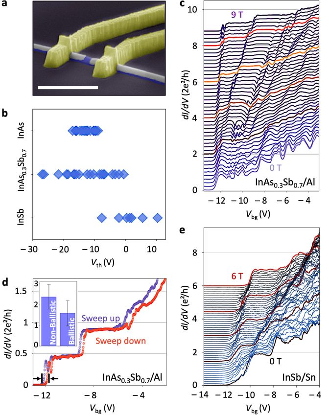
FIG. 4. Quantized transport in sharp-edged junctions.
the larger broadening profile of Al shadow edges, than
a, Pseudo colored SEM image of a typical single-junction
predicted by the hit-and-stick model, to the kinetically back-gated device. Scale bar is 1μm. b, Pinch-off voltage
driven equilibrium shape. For ls = 250 nm, the Sn and statistics for InAs, InAs0.3 Sb0.7 and InSb NW junction de-
Pb based junctions on InSb exhibit sharp edge shadows vices. c, Differential conductance as a function of gate voltage
as shown in Fig. 3g and Fig. 3h. In contrast to the and magnetic field of a InAs0.3 Sb0.7 /Al NW junction. d, Hys-
Al deposition, we used e-beam evaporation of Sn and Pb teresis of the device shown in (c) where sweep up and down
where the source opening WS depend on how the elec- follows closely. Inset is a comparison of a statistical value
of hysteresis between quantized and non-quantized devices.
tron beam are focused on the targeted materials. In the
e, Differential conductance as a function of gate voltage and
case of Sn, the effective area were visibly smaller than magnetic field for InSb/Sn NW junction.
the area of the total target, which means that the effec-
tive source opening WS and therefore ∆b will be smaller
for a given ls in case of "hit and stick" conditions. The
outgoing flux distribution can be estimated with a Gaus- tary information S9. This gate independent resistance
sian profile as discussed in 3a leading to a sharp edge contains mainly three contributions: contact resistance
flux profile in the transition region. Fig. 3g with line (Rc ), broadening resistance (R∆b ) and SE-SU interface
scale showing ∆b ∼ 13 nm confirms a sharp edge profile resistance (Rint ). In Fig. 3i, we can see that the
of Sn edge. Here, the measured sharpness may be under- InAs0.3 Sb0.7 /Al shadow junction resistance statistically
estimated due to the AFM tip diameter. On the other increases with increasing ls . It is surprising that the junc-
hand, for Pb based shadowing, the outgoing flux distri- tion resistance, R∆b depends on the slope of the Al to-
bution is more uniform from the source, as a result ∆b wards the junction, also for junctions without visible Al
for Pb based junction is larger than that of Sn, ∼ 75 nm islands, however the trend seems significant. For junc-
as extracted from line cuts in Fig. 3h. tions with dewetted Al islands it seem reasonable with
We study correlations between the junction trans- a reduced junction transparency due to potential varia-
parency and the critical parameter for the junction pro- tions caused by Al islands across the junctions. Using
file ls on the Al shadowed NWs. For this purpose standard four-probe measurements, the measured mean
we calculate the gate independent resistance R by fit- junction resistance is Rc = 0.8 kΩ as shown in Fig 3i.
ting the pinch-off curves as described in supplemen- Figure 3j shows conductance saturation of the devices7
decrease with increased ls . We attribute this effect to
the junctions with multiple Al grains for ls > 500 nm.
Unexpectedly, we also observe a trend of decreasing con-
ductance for ls < 250 nm, although Al grains do not form
within this range. We presume the profile of broadening
within that range may play a role on the conductance
deviation.
We further investigate the device performances of the
sharp edged junctions for InAs, InSb and InAs0.3 Sb0.7
NWs. Pseudo colored SEM image of a typical single
shadow junction device is shown in Fig 4a. In Fig
4b, we show the pinch-off voltages for Al based junc-
tion devices measured at 2 K. The pinch-off voltages
for InAs0.3 Sb0.7 /Al junctions show the widest span from
∼ −30V to ∼ 0V, while the InAs/Al junctions pinch-off
in the range of ∼ 0 to −10V. On the other hand, InSb/Al
junction devices show pinch-off at mainly positive Vg .
We ascribe the statistical differences to the band align-
ment between the semiconductor and the Al [41]. An
example of quantized conductance in a InAs0.3 Sb0.7 /Al
junction device is shown in Fig. 4c, where the conduc-
tance is measured as a function of Vg and magnetic field
(B). A general trend is that the conductance plateaus FIG. 5. Supercurrent and multiple Andreev reflections
are less pronounced at low B but gets gradually sharper in the sharp-edge junctions. a, Typical V I-curve for
with increasing field. This can be ascribed to lower elec- an InAs0.3 Sb0.7 /Al shadow Josephson junction (Device S#1).
tron back-scattering rates at higher B. The first subband The switching and retrapping currents are indicated. b, Dif-
splits into two spin-split subbands due to the Zeeman ef- ferential resistance as a function of current and gate poten-
tial. The black region corresponds to the zero-voltage state.
fect which leads to an energy difference gµB B, where g is
IC and normal state conductance gN measured at B⊥ = 0.3 T
the Landé-g factor and µB is Bohr’s magneton. For this are shown. c, IC vs. gN for all measured devices. Dashed lines
particular InAs0.3 Sb0.7 /Al device we see the emergence of are the theoretical expectations (see text). d, Voltage-biased
the spin-split sub-bands around B > 2.2 T. However, we measurement of the sub-gap structure of S#1 showing reso-
generally see the visible splitting appearing around B= nances of multiple Andreev reflections. The high-conductance
2-3 T. We speculate that the late emergence of visible region asymmetric around zero bias (∗) is related to a super-
spin-split bands are related to electron-electron interac- current branch enabled by the finite resistance of the cryostat
wiring (see text).
tion within the two subbands. The obtained quantized
values in Fig. 4c are lower than the predicted N e2 /h be-
cause of a constant contact resistance leading to plateaus
of 0.45 · 2e2 /h (the second at 0.9 · 2e2 /h and the third one Furthermore, unlike the sample shown in Fig. 4c, split-
is barely observed at 1.3 ± 0.5 · 2e2 /h), suggesting a non ting of the subband is visible immediately as the field is
changing contact resistance with gate due to the equal increased. A crossing of the first two spin-split subbands
quantized values for each subband. Figure 4d demon- is visible at around 2 T, characterized by the disappear-
strates a hysteresis which is much smaller than subband ance and re-emergence of a plateau at 2e2 /h. This effect
spacing in the device presented in Fig. 4c. The inset is expected due to the large Landé-g factor of InSb [42].
show a comparison of hysteresis statistics near the pinch- Figure 5 presents low temperature (T ∼ 20 mK) elec-
off region between quantized and non-quantized devices, trical measurements performed on seven InAs0.3 Sb0.7 /Al
where the quantized devices typically exhibit a slightly shadow JJs (S#1–S#7) with lj ∼ 100 nm. A single con-
smaller hysteresis ∼ 1.5 V, compare to others (∼ 2.3 V). tact to the Al shell is fabricated from Ti/Au normal
In Fig. 4e we examine sharp-edge InSb/Sn junction de- metal on either side of the shadow junction and split into
vice, with each trace offset by the value of the B. In con- separate bond-pads to allow for a pseudo four-terminal
trast to the InSb/Al junctions, the devices with Sn show configuration eliminating contributions from highly re-
a negative pinch-off voltage around −10 V, caused by sistive filters in the cryostat. The transmission of the
the different band alignment of Sn to InSb. In these de- junction is tunable by the back-gate potential Vg and
vices, after the subtraction of the filter resistances in the Fig. 5a shows typical V I-curves at Vg = 0 V for sample
fridge and a constant contact resistance, a clear plateau S#1. A zero-voltage state is observed corresponding to a
at 2e2 /h is visible even at zero field, suggesting a scat- switching current IC exceeding 200 nA with pronounced
tering length on the order of a few hundred nanometers. hysteresis between up/down sweep directions which is8
commonly observed in such devices and attributed to tions. The flexibility of the approach is exemplified with
heating effects or underdamped junction [43, 44]. Fig- the growth of InAs, InSb and InAs0.3 Sb0.7 NWs with in-
ure 5b shows the differential resistance as a function of situ shadowed junctions in Al, Sn and Pb. Based on the
I and Vg . The zero-resistance state is clearly observed performance statistics of field effect InAs0.3 Sb0.7 /Al de-
and IC decreases with Vg as the transparency of the n- vices we show that the quality of shadowed junctions are
type semiconductor weak link decreases towards pinch- significantly higher than the etched junctions. Further-
off at Vg ∼ −40 V. Also shown are the extracted gate- more, for the shadowed junctions we demonstrate that
dependence of the switching current IC (Vg ) and the nor- the junction transparency depends on the junction edge
mal state conductance gN (Vg ) measured at with a mag- profile. We conclude that the junctions with sharp edges
netic field B⊥ = 0.3 T applied perpendicular so the sub- has high transparency, exhibiting extremely large super-
strate and exceeding the critical field of the supercon- currents and easily resolved quantized conductance of the
ducting leads. The product of IC and RN = 1/gN is a lowest subbands. This study shows a path towards re-
typical voltage characterizing JJs and Fig. 5c shows IC liable gate-tunable operations in superconducting quan-
vs. gN for all devices where the range of gN is spanned tum networks.
by sweeping Vg . For samples S#2-7 the curves are ex-
tracted from the data included in supplementary infor-
mation S12. The dashed line labeled KO−1 (KO−2) ACKNOWLEDGEMENT
shows IC RN = π∆/2e (IC RN = π∆/e) expected for a JJ
in the short, quasi-ballistic and dirty (ballistic) regime The project is supported by European Union Hori-
with the mean-free path le
lj
ξ (le & lj , lj
ξ), zon 2020 research and innovation program under the
and a superconducting gap ∆ = 200 µeV expected for Al Marie Skłodowska-Curie Grant No. 722176 (INDEED),
and matching voltage-biased measurements discussed be- Microsoft Quantum and the European Research Coun-
low. ξ is the superconducting coherence length [45]. JJs cil (ERC) under Grant No. 716655 (HEMs-DAM). Au-
with semiconductor NWs weak links have been the sub- thors acknowledge C. B. Sørensen for maintenance and
ject of a large number of investigations since the original help with the MBE system. Thanks to Shivendra Upad-
work of Doh [43] and the critical currents in these devices hyay, Robert McNeil technical support in NBI cleanroom.
are generally much lower than the KO−1 and KO−2 pre- Also, thanks to Philippe Caroff, Keita Otani, Tomaš
dictions and Ic Rn significantly underestimates ∆ [46–48]. Stankevič, Emrah Yucelen for helpful discussions during
The origin of this suppression is unknown, but has been this research.
speculated to arise due to disorder and in-homogeneity or
to heavily underdamped junctions. For the InAs0.3 Sb0.7
shadow junctions studied here the critical currents are
COMPETING FINANCIAL INTERESTS
relatively high, and samples S#1 and S#2 follow ap-
proximately the KO−1 and the ballistic KO−2 result.
The remaining devices have suppressed IC for high RN The authors declare no competing financial interests.
indicating presence of channels with weak contribution
to the supercurrent. At lower resistance the increase in
IC with gN follows the KO−1 slope consistent with addi- SUPPLEMENTARY INFORMATION
tional channels with contribution to IC as predicted by
the model. We attribute these results to the high qual- The Supplementary Information is available at:
ity of the sharp edge InAs0.3 Sb0.7 /Al shadow junctions https://sid.erda.dk/share_redirect/FAS4l1InS3
and clean interface. For sample S#1 the phase-coherence
is confirmed by the voltage-biased measurement in Fig.
5d which shows a clear Vg -independent sub-gap struc-
ture which we attribute to multiple andreev reflections ∗
(MAR) as previously studied in NW JJ [43]. The reso- sabbir.khan@nbi.ku.dk
†
krogstrup@nbi.dk
nance resolved at lowest Vsd corresponds approximately [1] L. Casparis, M. R. Connolly, M. Kjaergaard, N. J. Pear-
to the n = 5th order MAR 2∆/ne process requiring five son, A. Kringhøj, T. W. Larsen, F. Kuemmeth, T. Wang,
coherent andreev reflection processes. Higher order MAR C. Thomas, S. Gronin, et al., Nature Nanotechnology 13,
processes may be present but are inaccessible in these 915 (2018).
measurements due to the cryostat line resistances ∼ 6 [2] T. W. Larsen, K. D. Petersson, F. Kuemmeth, T. S. Jes-
kΩ making the measurement an effective current-biased persen, P. Krogstrup, J. Nygård, and C. M. Marcus,
measurement at low applied voltages. Physical Review Letters 115, 127001 (2015).
[3] T. Karzig, C. Knapp, R. M. Lutchyn, P. Bonderson,
To conclude, we present a versatile single-step UHV M. B. Hastings, C. Nayak, J. Alicea, K. Flensberg,
crystal growth method to fabricate epitaxial SE-SU NWs S. Plugge, Y. Oreg, et al., Physical Review B 95, 235305
with high quality gate-tunable superconducting junc- (2017).9
[4] R. M. Lutchyn, J. D. Sau, and S. D. Sarma, Physical K. Watanabe, T. Taniguchi, and L. P. Kouwenhoven,
Review Letters 105, 077001 (2010). Nature Nanotechnology 13, 192 (2018).
[5] Y. Oreg, G. Refael, and F. von Oppen, Physical Review [25] C.-X. Liu, J. D. Sau, and S. Das Sarma, Physical Review
Letters 105, 177002 (2010). B 97, 214502 (2018).
[6] R. M. Lutchyn, E. P. A. M. Bakkers, L. P. Kouwenhoven, [26] E. J. Lee, X. Jiang, M. Houzet, R. Aguado, C. M.
P. Krogstrup, C. M. Marcus, and Y. Oreg, Nature Re- Lieber, and S. De Franceschi, Nature Nanotechnology
views Materials 3, 52 (2018). 9, 79 (2014).
[7] T. D. Stanescu and S. Tewari, Journal of Physics: Con- [27] H. Pan and S. D. Sarma, arXiv:1910.11413 (2019).
densed Matter 25, 29 (2013). [28] S. M. Albrecht, A. P. Higginbotham, M. Madsen,
[8] M. Leijnse and K. Flensberg, Semiconductor Science and F. Kuemmeth, T. S. Jespersen, J. Nygard, P. Krogstrup,
Technology 27, 11 (2012). and C. M. Marcus, Nature 531, 206 (2016).
[9] C. Nayak, S. H. Simon, A. Stern, M. Freedman, and [29] F. Nichele, A. C. C. Drachmann, A. M. Whiticar, E. C. T.
S. Das Sarma, Reviews of Modern Physics 80, 1083 O’Farrell, H. J. Suominen, A. Fornieri, T. Wang, G. C.
(2008). Gardner, C. Thomas, A. T. Hatke, P. Krogstrup, M. J.
[10] D. Aasen, M. Hell, R. V. Mishmash, A. Higginbotham, Manfra, K. Flensberg, and C. M. Marcus, Physical Re-
J. Danon, M. Leijnse, T. S. Jespersen, J. A. Folk, C. M. view Letters 119, 136803 (2017).
Marcus, K. Flensberg, et al., Physical Review X 6, [30] F. Krizek, T. Kanne, D. Razmadze, E. Johnson,
031016 (2016). J. Nygård, C. M. Marcus, and P. Krogstrup, Nano Let-
[11] P. Krogstrup, N. Ziino, W. Chang, S. Albrecht, M. Mad- ters 17, 6090 (2017).
sen, E. Johnson, J. Nygård, C. Marcus, and T. Jes- [31] S. Gazibegovic, D. Car, H. Zhang, S. C. Balk, J. A. Lo-
persen, Nature Materials 14, 400 (2015). gan, M. W. de Moor, M. C. Cassidy, R. Schmits, D. Xu,
[12] J. E. Sestoft, T. Kanne, A. N. Gejl, M. von Soosten, J. S. G. Wang, et al., Nature 548, 434 (2017).
Yodh, D. Sherman, B. Tarasinski, M. Wimmer, E. John- [32] D. J. Carrad, M. Bjergfelt, T. Kanne, M. Aagesen,
son, M. Deng, J. Nygård, C. Marcus, and P. Krogstrup, F. Krizek, E. M. Fiordaliso, E. Johnson, J. Nygård, and
Physical Review Materials 2, 044202 (2018). T. S. Jespersen, arXiv preprint arXiv:1911.00460 (2019).
[13] F. Krizek, J. E. Sestoft, P. Aseev, S. Marti-Sanchez, [33] D. Dalacu, A. Kam, D. G. Austing, and P. J. Poole,
S. Vaitiekėnas, L. Casparis, S. A. Khan, Y. Liu, T. c. v. Nano Letters 13, 2676 (2013).
Stankevič, A. M. Whiticar, A. Fursina, F. Boekhout, [34] P. Caroff, J. B. Wagner, K. A. Dick, H. A. Nilsson,
R. Koops, E. Uccelli, L. P. Kouwenhoven, C. M. Marcus, M. Jeppsson, D. Knut, L. Samuelson, L. R. Wallenberg,
J. Arbiol, and P. Krogstrup, Physical Review. Materials and L.-E. Wernersson, Small 4, 878 (2008).
2, 093401 (2018). [35] M. Pendharkar, B. Zhang, H. Wu, A. Zarassi, P. Zhang,
[14] Y. Liu, S. Vaitiekenas, S. Martí-Sánchez, C. Koch, C. Dempsey, J. Lee, S. Harrington, G. Badawy, S. Gaz-
S. Hart, Z. Cui, T. Kanne, S. A. Khan, R. Tanta, ibegovic, et al., arXiv preprint arXiv:1912.06071 (2019).
S. Upadhyay, et al., Nano Letters 20, 456 (2019). [36] G. W. Winkler, Q. Wu, M. Troyer, P. Krogstrup, and
[15] S. T. Gill, J. Damasco, B. E. Janicek, M. S. Durkin, A. A. Soluyanov, Physical Review Letters 117, 076403
V. Humbert, S. Gazibegovic, D. Car, E. P. Bakkers, P. Y. (2016).
Huang, and N. Mason, Nano Letters 18, 6121 (2018). [37] H. Potts, M. Friedl, F. Amaduzzi, K. Tang,
[16] V. Mourik, K. Zuo, S. M. Frolov, S. R. Plissard, E. P. G. Tütüncüoglu, F. Matteini, E. Alarcon Lladó, P. C.
A. M. Bakkers, and L. P. Kouwenhoven, Science 336, McIntyre, and A. Fontcuberta i Morral, Nano Letters
1003 (2012). 16, 637 (2016).
[17] A. Das, Y. Ronen, Y. Most, Y. Oreg, M. Heiblum, and [38] L. Vegard, Zeitschrift für Physik 5, 17 (1921).
H. Shtrikman, Nature Physics 8, 887 (2012). [39] W. Chang, S. Albrecht, T. Jespersen, F. Kuemmeth,
[18] L. P. Rokhinson, X. Liu, and J. K. Furdyna, Nature P. Krogstrup, J. Nygård, and C. Marcus, Nature Nan-
Physics 8, 795 (2012). otechnology 10, 232 (2015).
[19] M. Deng, C. Yu, G. Huang, M. Larsson, P. Caroff, and [40] P. Krogstrup, H. I. Jørgensen, E. Johnson, M. H. Madsen,
H. Xu, Nano Letters 12, 6414 (2012). C. B. Sørensen, A. F. i Morral, M. Aagesen, J. Nygård,
[20] A. D. K. Finck, D. J. Van Harlingen, P. K. Mohseni, and F. Glas, Journal of Physics D: Applied Physics 46,
K. Jung, and X. Li, Physical Review Letters 110, 126406 313001 (2013).
(2013). [41] S. Schuwalow, N. Schroeter, J. Gukelberger, C. Thomas,
[21] M. T. Deng, S. Vaitiekenas, E. B. Hansen, J. Danon, V. Strocov, J. Gamble, A. Chikina, M. Caputo,
M. Leijnse, K. Flensberg, J. Nygard, P. Krogstrup, and J. Krieger, G. C. Gardner, et al., arXiv preprint
C. M. Marcus, Science 354, 1557 (2016). arXiv:1910.02735 (2019).
[22] H. Zhang, C.-X. Liu, S. Gazibegovic, D. Xu, J. A. Lo- [42] I. van Weperen, S. R. Plissard, E. P. Bakkers, S. M.
gan, G. Wang, N. V. Loo, J. D. S. Bommer, M. W. A. d. Frolov, and L. P. Kouwenhoven, Nano letters 13, 387
Moor, D. Car, R. L. M. O. h. Veld, P. J. V. Veldhoven, (2013).
S. Koelling, M. A. Verheijen, M. Pendharkar, D. J. Pen- [43] Y.-J. Doh, J. A. van Dam, A. L. Roest, E. P. Bakkers,
nachio, B. Shojaei, J. S. Lee, C. J. Palmstrom, E. P. L. P. Kouwenhoven, and S. De Franceschi, science 309,
A. M. Bakkers, S. D. Sarma, and L. P. Kouwenhoven, 272 (2005).
Nature 556, 74 (2018). [44] H. Courtois, M. Meschke, J. Peltonen, and J. P. Pekola,
[23] J. Chen, P. Yu, J. Stenger, M. Hocevar, D. Car, S. R. Physical Review Letters 101, 067002 (2008).
Plissard, E. P. A. M. Bakkers, T. D. Stanescu, and S. M. [45] I. Kulik and A. Omel’Yanchuk, Sov. J. Low Temp.
Frolov, Science Advances 3, e1701476 (2017). Phys.(Engl. Transl.);(United States) 3 (1977).
[24] O. Gul, H. Zhang, J. D. S. Bommer, M. W. A. d. Moor, [46] J. Xiang, A. Vidan, M. Tinkham, R. M. Westervelt, and
D. Car, S. R. Plissard, E. P. A. M. Bakkers, A. Geresdi, C. M. Lieber, Nature Nanotechnology 1, 208 (2006).10
[47] H. Nilsson, P. Samuelsson, P. Caroff, and H. Xu, Nano
Letters 12, 228 (2012).
[48] K. Gharavi, G. W. Holloway, R. R. LaPierre, and
J. Baugh, Nanotechnology 28, 085202 (2017).You can also read