Fusing Nanowires into Thin Films: Fabrication of Graded-Heterojunction Perovskite Solar Cells with Enhanced Performance
←
→
Page content transcription
If your browser does not render page correctly, please read the page content below
Full paper
Perovskites                                                                                                                 www.advenergymat.de

Fusing Nanowires into Thin Films: Fabrication of Graded-
Heterojunction Perovskite Solar Cells with Enhanced
Performance
Yi Zhang, Hanjun Yang, Min Chen, Nitin P. Padture,* Ou Chen,* and Yuanyuan Zhou*

                                                                                                    state-of-the-art PSCs can be broadly divided
Perovskite solar cells (PSCs) have recently experienced a rapid rise in power                       into two types, viz., mesoscopic TiO2-
conversion efficiency (PCE), but the prevailing PSCs with conventional                              based PSCs and planar PSCs with only the
mesoscopic or planar device architectures still contain nonideal perovskite/                        compact TiO2 electron-transporting layer
                                                                                                    (ETL).[11–14] However, both types of devices
hole-transporting-layer (HTL) interfaces, limiting further enhancement in
                                                                                                    invariably contain a planar heterojunction
PCE and device stability. In this work, CsPbBr3 perovskite nanowires are                            formed at the interface between the perov-
employed for modifying the surface electronic states of bulk perovskite thin                        skite and the hole-transporting layer (HTL)
films, forming compositionally-graded heterojunction at the perovskite/HTL                          in PSCs. The energy level of the highest
interface of PSCs. The nanowire morphology is found to be key to achieving                          occupied molecular orbital (HOMO) of
                                                                                                    the commonly used HTL materials such
lateral homogeneity in the perovskite film surface states resulting in a near-
                                                                                                    as Spiro-OMeTAD, poly(3-hexylthiophene)
ideal graded heterojunction. The hidden role of such lateral homogeneity on                         and poly(triaryl amine) is about −5.1 eV,
the performance of graded-heterojunction PSCs is revealed for the first time.                       which does not match perfectly with the
The resulting PSCs show high PCE up to 21.4%, as well as high operational                           valence band maximum (VBM) of the pro-
stability, which is superior to control PSCs fabricated without CsPbBr3-                            totypical methylammonium lead triiodide
nanocrystals modification and with CsPbBr3-nanocubes modification. This                             (CH3NH3PbI3 or MAPbI3) perovskite,
                                                                                                    and also many other state-of-the-art halide
study demonstrates the promise of controlled hybridization of perovskite
                                                                                                    perovskite compositions.[15,16] This limits
nanowires and bulk thin films for more efficient and stable PSCs.                                   the open circuit voltage (VOC), and, thus,
                                                                                                    the PCE in these PSCs. Therefore, several
                                                                                                    studies in the literature have proposed ex
1. Introduction                                                              post facto incorporation of various materials at the perovskite/
                                                                             HTL interfaces to form graded-heterojunction, thereby reducing
Halide perovskite materials have emerged as a family of semi-                the energy level mismatch and enhancing the device perfor-
conductors that are catalyzing a revolution in the field of solar            mance.[17–20] However, this strategy always increases the com-
cells, as they offer the promise of low cost and exceptional                 plexity of the devices as well as the processing. In this context,
optoelectronic properties.[1–4] The record power conversion effi-            while the most-widely studied halide perovskite is MAPbI3, the
ciency (PCE) of perovskite-based solar cells (PSCs) has climbed              halide perovskite family has a wide composition space, which
rapidly to a certified 23.7%[5] since their invention in 2009.[4]            allows fine-tuning of electronic structures and properties in
Such rapid rise of PSCs has been mainly attributed to the signifi-           the perovskites themselves.[21–23] This unique feature of halide
cant effort and achievement in controlling the crystallization and           perovskite materials provides the opportunity to form graded
microstructures (grains and grain boundaries) of the perovskite              perovskite–HTL heterojunction simply through compositional
thin films.[6–10] The commonly used device architectures in the              engineering of perovskite thin films without the introduction of
                                                                             additional materials.[24] However, the fabrication of a perovskite
                                                                             layer with well-controlled graded compositions remains a signif-
Dr. Y. Zhang, M. Chen, Prof. N. P. Padture, Prof. Y. Zhou                    icant challenge. This is primarily because the use of orthogonal
School of Engineering                                                        solvents is required for the solution deposition of multilayer
Brown University
Providence, RI 02912, USA
                                                                             perovskite thin films, but all halide perovskites are generally
E-mail: nitin_padture@brown.edu; yuanyuan_zhou@brown.edu                     highly soluble in common polar solvents such as dimethylfor-
H. Yang, Prof. O. Chen                                                       mamide (DMF), dimethyl sulfoxide (DMSO), and N-methyl-
Department of Chemistry                                                      2-pyrrolidone.[25] Previous studies in the literature suggest the
Brown University                                                             feasibility of using perovskite nanocrystals (dispersed in the anti-
Providence, RI 02912, USA                                                    solvent used during the formation of the perovskite bulk thin
E-mail: ouchen@brown.edu
                                                                             films) to tackle this issue.[20,26–31] The most representative study
      The ORCID identification number(s) for the author(s) of this article
      can be found under https://doi.org/10.1002/aenm.201900243.
                                                                             is reported by Zai et al.,[29] who demonstrated the incorporation
                                                                             of CsPbBr3 nanocrystals (nanocube morphology) into a bulk
DOI: 10.1002/aenm.201900243                                                  MAPbI3 perovskite thin film, forming a graded heterojunction

Adv. Energy Mater. 2019, 1900243                                  1900243 (1 of 9)              © 2019 WILEY-VCH Verlag GmbH & Co. KGaA, Weinheim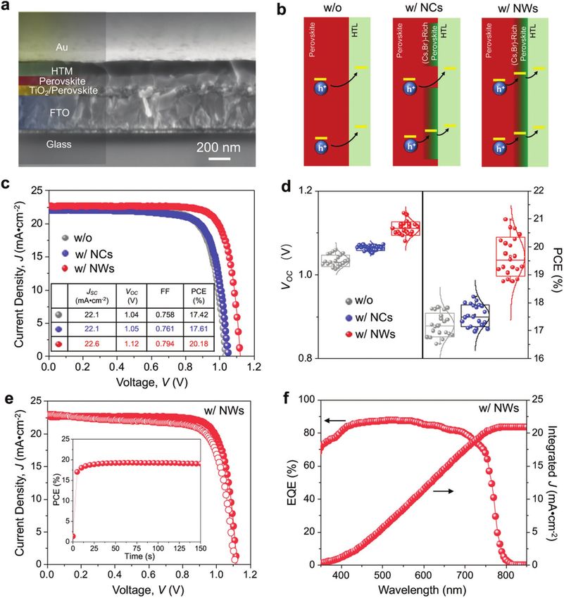
www.advancedsciencenews.com www.advenergymat.de
that improved the interfacial band alignment and the PSC PCE. diameter of 2.5 ± 0.5 nm (Figure 1b). Figure 1c shows UV–vis
Although this initial effort is very promising, in our study, we absorption and photoluminescence (PL) spectra of the CsPbBr3
have identified a hidden factor—lateral uniformity—in the as- NCs and NWs. Multiple electronic transition features with
formed graded heterojunction, which has a profound effect on sharp PL profiles indicate mono-dispersity in the CsPbBr3
the performance and stability of the final PSC devices. The use NCs and NWs, which is consistent with the TEM observations
of nanocrystals with the conventional nanocube morphology (Figure 1a,b). The significant blue-shift of both absorption and
leads only to incomplete passivation and mixed electronic states PL features of the CsPbBr3 NWs, as compared to the CsPbBr3
of the bulk perovskite film surface, thereby limiting the extent of NCs, is attributed to the stronger quantum confinement along
performance enhancement. Strikingly, by replacing nanocrystals the shorter dimension (2.5 nm) of the CsPbBr3 NWs, which is
with nanowires, this issue is well addressed with the ready and consistent with previous observations.[35,36] Figure 1d presents
reproducible formation of laterally homogeneous heterojunc- X-ray diffraction (XRD) patterns of CsPbBr3 NCs and NWs,
tions, resulting in significantly improved PSC PCE and opera- both of which show characteristic broad 110 and 200 peaks,
tional stability. More importantly, this method is generic, and confirming the purity of the perovskite phase. The XRD peak
it can be used for the fabrication of PSCs with various perov- broadening in the CsPbBr3 NCs results in a size estimation of
skite thin film compositions. For example, the incorporation 7.8 nm using the Scherer equation (see Figure S1, Supporting
of CsPbBr3 nanowires into the mixed-cation halide perovskite Information), which is consistent with the TEM results. Note
(MA0.3FA0.7PbI3) bulk thin films leads to PSCs with PCE as high that the peak-broadening method cannot be applied reliably to
as 21.4%. CsPbBr3 NWs due to their high aspect ratios.
The as-synthesized CsPbBr3 NCs or NWs were dispersed
in chlorobenzene, forming colloidal suspension for use in the
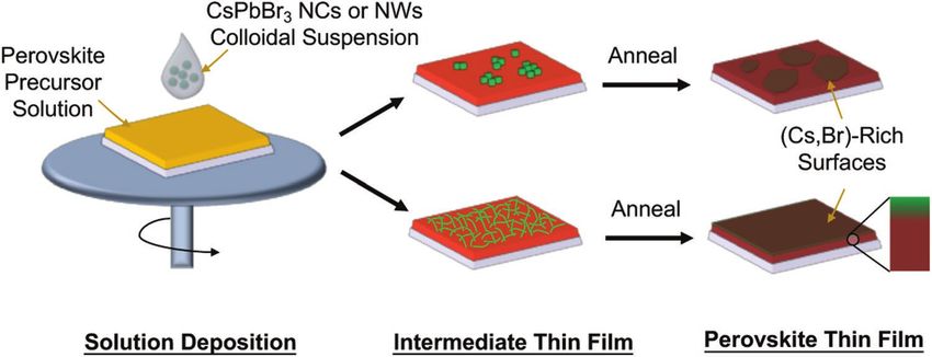
2. Results and Discussion thin film processing. The processing method is illustrated sche-
matically in Figure 2. First, the perovskite precursor solution (in
CsPbBr3 perovskite nanocubes (NCs) and nanowires (NWs) DMSO) is spread on the substrate, and then spin-coated. During
were synthesized using modified methods that have been the spin-coating process, a drop of CsPbBr3 NCs or NWs col-
reported in the literature.[28,32–34] CsPbBr3 is chosen due to loidal suspension is dripped. The dripped nanocrystals (NCs or
its structural similarity with MAPbI3, small lattice mismatch NWs) not only serve as heterogeneous nucleation sites for the
(5.9%), high stability, and ease of synthesis. Figure 1a and crystallization of the perovskite-solvent adduct thin films, but
b are transmission electron microscope (TEM) images of the are also anchored near the thin film surface. The second step
as-synthesized CsPbBr3 NCs and NWs, respectively, showing is thermal annealing, which “fuses” the CsPbBr3 NCs or NWs
high uniformity in size and shape. The average edge length into the perovskite thin film via diffusion, inducing a gradation
of CsPbBr3 NCs is determined to be 8.5 ± 0.7 nm (Figure 1a). of CsPbBr3-rich at the top to CsPbBr3-lean toward the bottom of
The average length of the NWs is 95 ± 42 nm, with an average the perovskite film.[37] This fabrication method is similar to what
Figure 1. Bright-field TEM images of schematic illustrations (insets). a) CsPbBr3 NCs and b) NWs. c) UV–vis absorption (solid lines) and PL (dashed
lines) spectra of CsPbBr3 NCs and NWs. d) Indexed XRD patterns of CsPbBr3 NCs and NWs.
Adv. Energy Mater. 2019, 1900243 1900243 (2 of 9) © 2019 WILEY-VCH Verlag GmbH & Co. KGaA, Weinheim
www.advancedsciencenews.com www.advenergymat.de Figure 2. Schematic illustration showing the preparation of perovskite thin films with graded incorporation of CsPbBr3 nanocrystals at the top film surface. The effect of nanocrystal morphology (either nanowire or nanocube) is also illustrated. was recently reported by Zai et al.[29] However, the significant with better surface coverage. The size of the NWs may influence finding here is that the morphology of the CsPbBr3 nanocrystals this thin film modification process and final device perfor- plays an important role in determining the distribution of their mance, but that study is a topic for future research. surface incorporation, which has a profound effect on the prop- It is worth noting that Chen et al.[38] have also used CsPbBr3 erties/performance of the final perovskite thin films and PSCs. NWs in the context of modifying the MAPbI3/HTL interface. Specifically, in the case of NCs incorporation, the NCs tend to However, in that study, the CsPbBr3 NWs were postdeposited aggregate during the dripping step, which correspondingly on as-prepared solid MAPbI3 perovskite thin film, and only results in a spatially inhomogeneous distribution on the film physically located on the film surface. Their objective was quite surface. In the case of NWs, owing to their superior disper- different from that of the present study, where a CsPbBr3-NWs sion (Figure S2, Supporting Information), NWs form uniform assembly was created at the interface to serve as a “grating” for interconnected network on the film surface, which then diffuses improved light harvesting and efficient fluorescence resonance evenly into the film during annealing to form a uniform layer energy transfer.[38] Figure 3. Top-view SEM images of the MAPbI3 perovskite thin films. a) without CsPbBr3 nanocrystals, b) with CsPbBr3-NCs incorporation, and c) with CsPbBr3-NWs incorporation. d,e) Indexed XRD patterns and f) time-resolved PL spectra of MAPbI3 perovskite thin films without and with CsPbBr3 NCs or NWs incorporation. Adv. Energy Mater. 2019, 1900243 1900243 (3 of 9) © 2019 WILEY-VCH Verlag GmbH & Co. KGaA, Weinheim
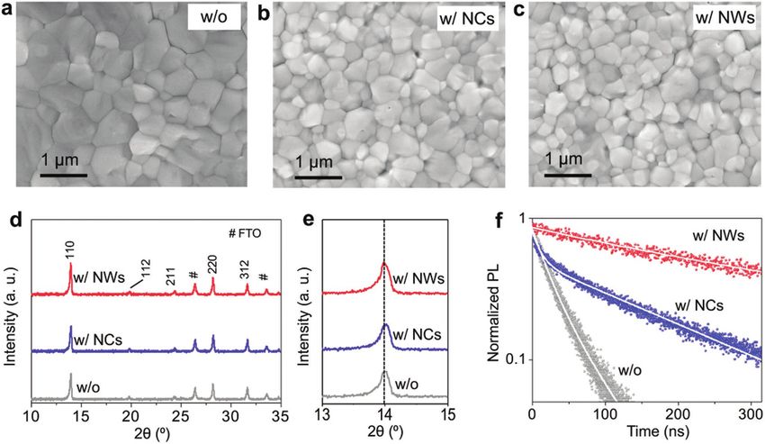
www.advancedsciencenews.com                                                                                                 www.advenergymat.de

Figure 4. KPFM surface potential mapping of the MAPbI3 perovskite films. a) without nanocrystals, b) with CsPbBr3-NCs incorporation, and c) with
CsPbBr3-NWs incorporation. d) The surface potential variation along the white dashed lines drawn in (a,b,c). e) Illustration of the methodology of
glancing-angle XRD. f) Glancing-angle XRD patterns of the MAPbI3 thin film with CsPbBr3-NWs incorporation measured at different glancing angles.

   Figure 3a–c shows top-view scanning electron microscope                 or NWs incorporation process. The 110 XRD peak in Figure 3e
(SEM) images of the MAPbI3 perovskite thin films without                   shows no obvious shift, consistent with the low concentra-
nanocrystal, with CsPbBr3-NCs incorporation, and CsPbBr3-                  tion of CsPbBr3 in the entire bulk of the MAPbI3 perovskite
NWs incorporation, respectively. The nanocrystal-free MAPbI3               thin film. The lack of separate XRD peaks and the absence
perovskite thin film shows typical compact, polycrystalline                of nanocrystals in top-view SEM suggest that the introduced
grain morphology with a mean grain size of 620 nm. In the                  CsPbBr3 has been alloyed into the bulk perovskite layer without
NCs- and NWs-incorporated cases, the overall morphology is                 phase segregation. The time-resolved PL spectra in Figure 3f
about the same, but the mean grain size is slightly reduced to             show much slower PL decay rates after NCs or NWs incorpo-
555 and 460 nm, respectively. The grain size statistics obtained           ration. The average PL lifetimes (τAvg) for the nanocrystal-free,
using image analysis are reported in Figure S3 in the Sup-                 NCs-incorporated, and NWs-incorporated cases are 37, 126, and
porting Information. Correspondingly, the surface roughness                589 ns, respectively. The PL fitting results are shown in Table S1
(15.3 nm for the nanocrystal-free case) of the MAPbI3 perov-               in the Supporting Information. As discussed above, the grain-
skite thin film is also reduced to 10.2 nm for the NCs case and            boundary density is slightly increased after the nanocrystals
7.5 nm for the NWs case, as measured using atomic force                    incorporation. Thus, the enhanced PL property is attributed to
microscopy (AFM) (Figure S4, Supporting Information). These                the beneficial passivation of the film surfaces induced by the
morphology changes induced by nanocrystals incorporation                   nanocrystals incorporation, where the more uniform surface-
can be attributed to the fact that the nanocrystals serve as               passivation in the NWs case leads to the longest PL lifetime.
additional heterogeneous nucleation sites that can boost the                  Albeit having the same chemical composition, the spatial
nucleation rate during the MAPbI3 perovskite crystallization               uniformity of nanocrystal distribution is influenced significantly
process.[7] Furthermore, in the NWs-incorporated case, their               by the morphology of nanocrystals. Since the concentration of
higher dispersion in solvent is likely to enhance this effect              CsPbBr3 nanocrystals is in fact lower than the detection limits
on the film crystallization. Figure 3d shows XRD patterns                  of typical analytical tools (energy dispersive spectroscopy, etc.),
of MAPbI3 perovskite thin films without nanocrystals, with                 surface potential maps of the MAPbI3 perovskite thin films
CsPbBr3-NCs incorporation, and with CsPbBr3-NWs incorpora-                 under continuous illumination with and without nanocrystals-
tion. All the XRD patterns show the characteristic reflections             incorporation were obtained using Kelvin-probe force micros-
of the MAPbI3 perovskite (indexed), indicating that no sec-                copy (KPFM). The results are presented in Figure 4a–c. Without
ondary crystalline phases are introduced as a result of the NCs            nanocrystals, the surface potential is relatively homogeneous

Adv. Energy Mater. 2019, 1900243                               1900243 (4 of 9)                © 2019 WILEY-VCH Verlag GmbH & Co. KGaA, Weinheim
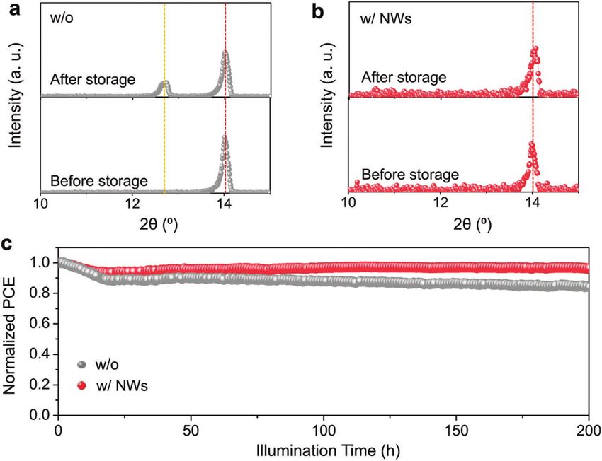
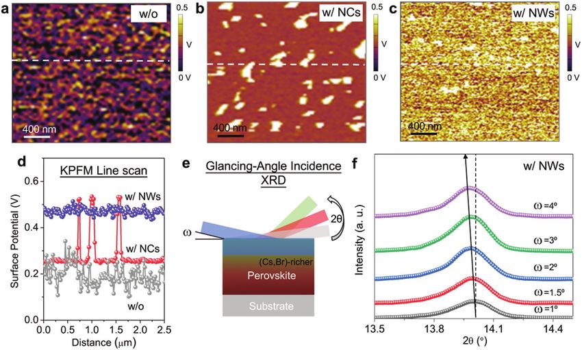
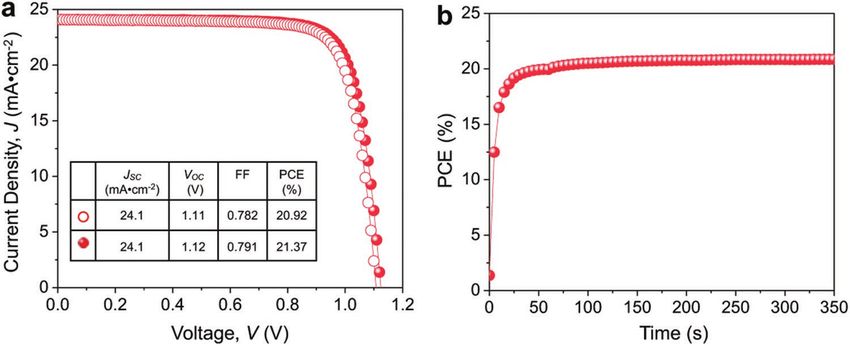
www.advancedsciencenews.com                                                                                       www.advenergymat.de

across the film surface. When incorporated with CsPbBr3             current density measured from the J–V curves is consistent with
NCs, some areas of the film surface show higher potentials,         the integrated current density (21.3 mA cm−2) from the external
reflecting an inhomogeneous passivation of the film. However,       quantum efficiency (EQE) measurement shown in Figure 5f.
when CsPbBr3 NWs are incorporated, the surface potential            Since the device exhibits typical hysteresis, the power output at
shows a uniform increase across the entire film surface. These      the maximum power point (inset of Figure 5e) is monitored.
results strongly support our hypothesis that only CsPbBr3 NWs       The PCE of the device stabilizes at ≈19%, comparing favorably
enable the uniform incorporation across the entire film sur-        with that extracted from the reverse-scan J–V curve.
face (Figure 2), which is consistent with the PL lifetime results      In addition to the PCE enhancement, the chemical sta-
shown in Figure 3f. The line-profiles of the surface-potential      bility of the MAPbI3 perovskite is also greatly boosted, which
mapping images clearly reveal the surface potential varia-          represents another important advantage of the CsPbBr3-NWs-
tions for the three films as shown in Figure 4d. To delineate       incorporated perovskite films. Figure 6a,b shows representative
the depth profile of the CsPbBr3 nanocrystals incorporation,        XRD patterns of the MAPbI3 perovskite thin films (nanocrystal-
glancing-angle (ω) XRD analysis (Figure 4e) was performed.          free and NWs-incorporated) before and after 200 h storage under
Figure 4f shows the ω-dependent XRD patterns of the CsPbBr3         controlled conditions (70% RH, 25 °C). While the nanocrystal-
NWs-incorporated MAPbI3 perovskite thin film. It is evident         free MAPbI3 perovskite thin film shows notable decomposition
that with an increase in ω, the 110 peak position of MAPbI3         to PbI2 after storage, the NWs-incorporated film maintains its
shifts gradually to lower 2θ angles. This observation suggests      good phase purity as well as the compact grain morphology (see
that there is a gradual expansion of the crystal lattice from       Figure S6, Supporting Information). It is most likely that the
the top surface to the bulk film, consistent with the graded-       NW-incorporation not only passivates the surface defects (see
incorporation of CsPbBr3 into the MAPbI3 perovskite thin film.      Figure 3f) and thus slows the moisture ingression kinetics, but
   PSC devices using the three types of MAPbI3 perovskite thin      also enhances the ionic and/or covalent bonding by incorpo-
films (without nanocrystals, and with NCs or NWs incorpora-         rating ions (Cs+ and Br−) with smaller radii in the crystalline
tion) were fabricated by sandwiching the thin films between         structure (see Figure 4f). The long-term device stability is also
an FTO/TiO2 anode and a Spiro-OMeTAD/Au cathode. The                evaluated by operating the PSCs at maximum-power-points con-
typical device architecture is shown in Figure 5a. A scheme         tinuously under one-sun illumination (unencapsulated, flowing
of the relative energy-levels is shown in Figure 5b to illus-       N2 atmosphere, 40 °C). While the nanocrystal-free PSC shows a
trate the benefit of the CsPbBr3 nanocrystals incorporation in      decrease of about 16% in PCE after 200 h, only a 4% PCE loss
MAPbI3 thin films of PSCs. In the nanocrystal-free case, there      is observed for the NWs-incorporated PSC, demonstrating the
is a notable energy-level mismatch between HTM HOMO and             promise of CsPbBr3-NWs incorporation in enhancing the device
MAPbI3 perovskite VBM levels, which leads to insufficient           stability of PSCs. In addition, the PCE evolution of both PSCs
VOC in PSC devices. After the CsPbBr3-nanocrystals incorpora-       with and without CsPbBr3-NWs incorporation as a function of
tion, the VBM of the MAPbI3 perovskite surface is increased         storage time under the same ambient conditions was also mon-
by 0.09 eV (see Figure S5, Supporting Information). However,        itored, confirming the enhanced ambient stability in the case of
such VBM increase is not uniform for the NC-incorporated            NWs incorporation (Figure S7, Supporting Information).
case, which is related to the nonuniform incorporation as              In order to demonstrate the generality of the NWs-incorpo-
discussed above. This nonuniform surface incorporation will         ration approach for making high-efficiency PSCs, we have used
result in mixed-electronic structures of the film surface, and,     this approach for modifying the perovskite/HTM heterojunction
thus, the VOC enhancement in the final devices is limited. In       in MA0.3FA0.7PbI3-composition PSCs. This composition of
addition to the enhanced carrier extraction, the laterally uni-     perovskite is known to harvest sunlight more efficiently in
form incorporation by NWs also provides improved surface            the infrared-red region.[39] The as-fabricated PSCs based on
passivation according to time-resolved PL (Figure 3f), which        this mixed-cation halide perovskite show obvious performance
is possibly another source for improved device performance.         enhancement, as compared to PSCs without CsPbBr3 NWs
Figure 5c shows the typical current density–voltage (J–V)           incorporation, and also PSCs with CsPbBr3 NCs incorpora-
curves (reverse scan) for the PSCs without nanocrystals incor-      tion (Figure S8, Supporting Information). The “champion”
poration, with NCs or NWs incorporation, respectively. The          device (Figure 7a) shows JSC of 24.1 mA cm−2, VOC of 1.12 V,
device with NCs shows VOC of 1.05 V, which is slightly higher       FF of 0.791, and PCE of 21.4% under reverse scan, and JSC of
than that of 1.04 V for the nanocrystal-free device. However,       24.1 mA cm−2, VOC of 1.11 V, FF of 0.782, and PCE of 20.9%
when NWs are used, the homogeneous surface incorporation            under forward scan. The PCE output at maximum-power-
(as discussed above) brings up the VBM and thus the device          point (V = 0.95 V) is stabilized at ≈21% (Figure 7b), which
VOC to 1.12 V (Figure 5c). Consequently, the overall PCE is         approaches that for those state-of-the-art PSCs.[13,15,24] Thus,
boosted to 20.18%, compared to 17.42% for the nanocrystal-          the NWs-incorporation approach is shown to complement the
free PSC and 17.61% for the NCs-incorporated PSC (see inset         popular perovskite “composition engineering” methods.[3]
Table in Figure 5c). Figure 5d shows the VOC and PCE statis-
tics for the three cases, confirming the high reproducibility of
the device performance results. The J–V hysteresis for a typ-       3. Conclusions
ical PSC with NWs incorporation is shown in Figure 5e. The
PCE measured using forward and reverse scans are 20.09%             Graded heterojunction PSCs with high lateral uniformity are
(JSC: 22.60 mA cm−2; VOC: 1.124 V; FF: 0.791) and 18.75% (JSC:      reported here for the first time by incorporating CsPbBr3 NWs
22.59 mA cm−2; VOC: 1.113 V; FF: 0.746), respectively. The          during the processing of bulk perovskite thin films. Our study

Adv. Energy Mater. 2019, 1900243                          1900243 (5 of 9)            © 2019 WILEY-VCH Verlag GmbH & Co. KGaA, Weinheim
www.advancedsciencenews.com www.advenergymat.de Figure 5. a) Cross-sectional SEM image of the PSC using CsPbBr3 NW-incorporated MAPbI3 perovskite thin film. b) Schematic representation of the hole-extraction in the PSC without nanocrystals, with CsPbBr3-NCs incorporation, and with CsPbBr3-NWs incorporation. c) J–V curves (reverse-scan) and (d) the corresponding PCE statistics of the PSCs without nanocrystal, with CsPbBr3-NCs incorporation, and with CsPbBr3-NWs incorporation. e) J–V hysteresis of the PSC with CsPbBr3-NWs incorporation. Inset is the maximum-power-point power output of this PSC. f) EQE and integrated current density of the “champion” PSC. reveals that the nanowire morphology is of vital importance can lead to enhanced passivation of the bulk perovskite thin for achieving uniform lateral incorporation of CsPbBr3 nano film surfaces, stabilizing the PSCs. The incorporation of nano- crystals into bulk perovskite thin films that favors the formation wires within bulk perovskite thin films surfaces represents a of near-ideal perovskite/HTL heterojunction for high-efficiency new strategy for making efficient and stable PSCs with engi- PSCs. In addition, the surface-incorporation by CsPbBr3 NWs neered interfaces. Adv. Energy Mater. 2019, 1900243 1900243 (6 of 9) © 2019 WILEY-VCH Verlag GmbH & Co. KGaA, Weinheim
www.advancedsciencenews.com                                                                                                         www.advenergymat.de

Figure 6. Long-term stability of the perovskite thin films and devices. Representative XRD patterns of the MAPbI3 perovskite thin films before and
after 200 h storage under controlled conditions (70 RH%, 25 °C): a) without nanocrystals, b) with CsPbBr3-NWs incorporation. The yellow and red
dashed lines indicate the peak positions of 001 reflection of the PbI2 crystal phase and 110 reflection of the MAPbI3 perovskite phase, respectively.
c) Long-term operational stability (under continuous one-sun illumination, unencapsulated, flowing N2 atmosphere, 40 °C) of PSC devices made
without nanocrystals and with CsPbBr3-NWs incorporation.

4. Experimental Section                                                         modifications. Briefly, 138 mg of PbBr2 (Sigma-Aldrich, USA) was
                                                                                dissolved in 10 mL of 1-octadecene with 1 mL of oleic acid and 1 mL
   Synthesis of Perovskite Nanocrystals: Cesium-oleate was first                of oleylamine (technical grade, 70%, Sigma-Aldrich, USA). The mixture
synthesized by heating 0.625 mmol of Cs2CO3 (Sigma-Aldrich, USA)                was degassed under vacuum at 100 °C for 1 h before heating up to
with 2.0 mmol of oleic acid (technical grade, 90%, Sigma-Aldrich,               170 °C under flowing N2, and then 0.8 mL of cesium-oleate solution
USA) in 10 mL 1-octadecene (technical grade, 90%, Sigma-Aldrich,                was rapidly injected into the solution. Within 30 s after injection,
USA) at 80 °C under vacuum for 30 min. Subsequently, the reaction               the reaction solution was cooled down to room temperature in an
mixture was heated to 150 °C until the solids were fully dissolved.             ice-water bath. NCs were separated by centrifuge at 8000 rpm for
The solution was cooled down to room temperature and stored as a                5 min, and they redispersed in hexane (Fisher Scientific, USA). The
stock solution for further use. The CsPbBr3 perovskite NCs were then            resultant NCs were purified by two rounds of precipitation-redispersion
synthesized using a method reported in the literature,[28] with some            process using ethyl acetate (Fisher Scientific, USA) and hexane. The

Figure 7. a) J–V curves at reverse and forward scans of the “champion” PSC device based on CsPbBr3-NWs incorporated MA0.7FA0.3PbI3-composition
bulk perovskite thin films. Solid circle: reserve scan; open circle: forward scan. Inset table includes the extracted J–V parameters. b) Stabilized maximum-
power-point power output of this PSC.

Adv. Energy Mater. 2019, 1900243                                    1900243 (7 of 9)                  © 2019 WILEY-VCH Verlag GmbH & Co. KGaA, Weinheim
www.advancedsciencenews.com www.advenergymat.de
purified NCs were redispersed in hexane or chlorobenzene (Fisher 36 µL of 4- tertbutylpyridine were added. The HTL was formed by
Scientific, USA) forming a clear solution for further use. CsPbBr3 NWs spin-coating the solution at 4000 rpm for 20 s. Finally, 80 nm thick Au
were synthesized also using a method reported in the literature,[29] electrode was deposited on the top of HTL by thermal evaporation. The
with some modifications. In a glass vial, 1.25 mL of hexane was mixed J–V characteristics of the PSCs were measured using a 2400 Sourcemeter
with 0.125 mL of oleic acid and 0.125 mL of oleylamine, to that vial (Keithley, USA) under simulated one-sun AM1.5G 100 mW cm−2 intensity
0.1 mL of cesium-oleate solution was added. Swiftly added to that (Oriel Sol3A Class AAA, Newport, USA), under both reverse (from VOC
reaction solution was 0.2 mL of 0.4 m PbBr2 in DMF (Sigma-Aldrich, to JSC) and forward (from JSC to VOC) scans. The step voltage was 5 mV
USA) under vigorous stirring. At 10 s after injection, 5 mL of acetone with a 10 ms delay time per step. The maximum-power output stability
was added to the vial. The solution was allowed to react for 5 min of PSCs was measured by monitoring the J output at the maximum-
before the NWs were separated from the solution using centrifuge power-point V bias (deduced from the reverse-scan J–V curves) using the
at 6000 rpm for 5 min. The resulting NWs were then redispersed in 2400 SourceMeter. A typical active area of 0.12 cm2 was defined using a
hexane or chlorobenzene for further use. nonreflective mask for the J–V measurements. The stabilized output PCE
Preparation of Perovskite Thin Films: MAPbI3 precursor solution was calculated using the following relation: PCE = J (mA cm−2) × V (V))/
(1.3 m) was prepared by dissolving MAI and PbI2 in 1:1 molar ratio in (100 (mW cm−2). A shutter was used to control the one-sun illumination
DMF. Similarly, MA0.3FA0.7PbI3 precursor solution (1.3 m) was prepared on the PSC. The EQE spectra were obtained using a quantum-efficiency
by dissolving MAI, FAI, and PbI2 in 0.3:0.7:1 molar ratio in DMF measurement system (Oriel IQE 200B, Newport, USA). The PSC stability
(Sigma-Aldrich, USA). Subsequently, the precursor solutions were spin- was evaluated by measuring the J–V characteristics of PSCs after storing
coated onto substrates at 1000 rpm for 10 s, followed by 5000 rpm for the cells in controlled environment for a certain period of time in a
30 s. After spinning at 5000 rpm for 10 s, 100 µL of chlorobenzene was climate chamber (HPP110, Memmert, Germany). Unencapsulated PSCs
dripped on to the film. The as-formed solid thin films were annealed at were placed in a sealed holder with a transparent glass cover. A flow of N2
100 °C for 20 min, resulting in MAPbI3 or MA0.3FA0.7PbI3 perovskite thin gas was continuously passed through the holder to minimize the water
films. For depositing MAPbI3 or MA0.3FA0.7PbI3 perovskite thin films with and oxygen content. J–V curves were measured every 2 h under one-sun
CsPbBr3 NCs and NWs incorporation, 1 mg ml−1 CsPbBr3 NCs or NWs illumination while maintaining the PSCs temperature at ≈40 °C. Between
colloidal suspension in chlorobenzene were, respectively, used for the the J–V measurements, the PSCs were biased at maximum-power-point
dripping instead of the pure chlorobenzene solvent. voltages using a potentiostat under continuous one-sun illumination.
Nanocrystals Characterization: UV–vis absorption spectra were Additional stability experiments were performed, where unencapsulated
measured using a spectrophotometer (Cary 5000, Agilent Technologies, PSCs were stored under laboratory ambient conditions, and their PCEs
USA). PL spectra of CsPbBr3 NCs and NWs were measured on a under one-sun illumination were measured about every 25 h.
fluorescence spectrometer using 365 nm excitation (FS5, Edinburgh
Instruments, UK). TEM characterization was performed using a 2100F
TEM (JEOL, Japan) operated at 200 kV. For the TEM sample preparation,
the NCs or NWs were directly drop-cast onto TEM grids and dried Supporting Information
under ambient conditions. Powder XRD patterns were obtained on a Supporting Information is available from the Wiley Online Library or
diffractometer (D8 Discovery, Bruker, Germany) using Cu Kα radiation. from the author.
The CsPbBr3 NCs and NWs samples were prepared by drop-casting onto
glass slides for XRD characterization.
Thin Film Characterization: XRD patterns were acquired using a high-
resolution diffractometer (D8 Advance, Bruker, Germany) with Cu Kα Acknowledgements
radiation. The glancing incidence angle XRD measurements were carried
out with glancing angle ranging from 1o to 4o. UV–vis spectra were Y.Z. and H.Y. contributed equally to this work. Y.Z., N.P.P., O.C.,
obtained using a spectrophotometer (UV-2600, Shimadzu, Japan). The Y.Z., and M.C. acknowledge the support from the National Science
microstructures were observed using a SEM (LEO 1530VP, Carl Zeiss, Foundation (OIA-1538893). H.Y. and O.C. acknowledge the support
Germany). Ultraviolet photoelectron spectroscopy (UPS) spectra were from the Brown University startup funds. Y.Z., O.C., Y.Z., and H.Y. also
recorded on a UPS system (5600, PHI, USA). The steady-state and time- thank the support from the Brown University's Institute for Molecular
resolved PL spectra were recorded using a lab-built spectrophotometer and Nanoscale Innovation (IMNI) Seed fund. The authors thank
under 395 nm excitation. The PL lifetime was obtained by fitting the Mr. W. Li for his experimental assistance.
time-resolved PL spectra using biexponential decay functions. The AFM
measurements with white LED were performed using a versatile AFM
(MFP-3D Origin, Asylum Research, USA) in contact mode using conducting Conflict of Interest
Ti/Ir-coated probe tips (ASYELEC.01-R2, Asylum Research, USA).
Device Fabrication and Testing: Patterned FTO glass substrates The authors declare no conflict of interest.
(Hartford Glass, USA) were cleaned sequentially with detergent
solution, acetone, and isopropanol. TiO2 ETL (20 nm) was deposited
by spray pyrolysis at 450 °C. The stock solution used for the spray
pyrolysis was prepared by mixing 0.2 mL of titanium diisopropoxide
Keywords
bis(acetylacetonate) (TAA) solution (Sigma-Aldrich, USA) with 6 mL of halide perovskites, heterojunction, morphology control, nanocrystals,
anhydrous ethanol. A 200 nm mesoporous TiO2 layer was the deposited solar cells
by spin-coating (2000 rpm for 10 s) using a commercial TiO2 paste
(Dyesol-30NRD, Dyesol, Australia) diluted in ethanol (weight ratio of Received: January 21, 2019
the TiO2 paste to ethanol was 9:1). The as-coated TiO2 thin film was Revised: February 18, 2019
dried on a hotplate at 80 °C, and then sintered at 500 °C for 20 min. Published online:
This was followed by the deposition of the perovskite layer according
to the procedure described above. The HTL solution was prepared by
dissolving 91 mg of Spiro-OMeTAD (Merck) with additives in 1 mL of
chlorobenzene. To this solution, 21 µL of Li-bis(trifluoromethanesulfonyl)
imide from the stock solution (520 mg in 1 mL of acetonitrile), 16 µL of [1] N.-G. Park, M. Grätzel, T. Miyasaka, K. Zhu, K. Emery, Nat. Energy
FK209 [tris(2-(1H-pyrazol-1-yl)-4-tert-butylpyridine)-cobalt(III) tris(bis 2016, 1, 16152.
(trifluoromethylsulfonyl)imide) (375 mg in 1 mL of acetonitrile), and [2] H. J. Snaith, Nat. Mater. 2018, 17, 372.
Adv. Energy Mater. 2019, 1900243 1900243 (8 of 9) © 2019 WILEY-VCH Verlag GmbH & Co. KGaA, Weinheimwww.advancedsciencenews.com www.advenergymat.de
[3] J.-P. Correa-Baena, M. Saliba, T. Buonassisi, M. Grätzel, A. Abate, [22] Y. Zhou, Z. Zhou, M. Chen, Y. Zong, J. Huang, S. Pang,
W. Tress, A. Hagfeldt, Science 2017, 358, 739. N. P. Padture, J. Mater. Chem. A 2016, 4, 17623.
[4] A. Kojima, K. Teshima, Y. Shirai, T. Miyasaka, J. Am. Chem. Soc. [23] M. Chen, M.-G. Ju, A. D. Carl, Y. Zong, R. L. Grimm, J. Gu,
2009, 131, 6050. X. C. Zeng, Y. Zhou, N. P. Padture, Joule 2018, 2, 558.
[5] NREL Chart of Best Research-Cell Efficiencies, https://www.nrel. [24] D. Luo, W. Yang, Z. Wang, A. Sadhanala, Q. Hu, R. Su, R. Shivanna,
gov/pv/cell-efficiency.html (accessed: February 2019). G. F. Trindade, J. F. Watts, Z. Xu, T. Liu, K. Chen, F. Ye, P. Wu,
[6] S. D. Stranks, P. K. Nayak, W. Zhang, T. Stergiopoulos, H. J. Snaith, L. Zhao, J. Wu, Y. Tu, Y. Zhang, X. Yang, W. Zhang, R. H. Friend,
Angew. Chem., Int. Ed. 2015, 54, 3240. Q. Gong, H. J. Snaith, R. Zhu, Science 2018, 360, 1442.
[7] Y. Zhou, O. S. Game, S. Pang, N. P. Padture, J. Phys. Chem. Lett. [25] J.-W. Lee, Z. Dai, T.-H. Han, C. Choi, S.-Y. Chang, S.-J. Lee,
2015, 6, 4827. N. De Marco, H. Zhao, P. Sun, Y. Huang, Y. Yang, Nat. Commun.
[8] Y. Zong, Y. Zhou, Y. Zhang, Z. Li, L. Zhang, M.-G. Ju, M. Chen, 2018, 9, 3021.
S. Pang, X. C. Zeng, N. P. Padture, Chem 2018, 4, 1404. [26] H. Bian, D. Bai, Z. Jin, K. Wang, L. Liang, H. Wang, J. Zhang,
[9] Y. Zhang, Z. Fei, P. Gao, Y. Lee, F. F. Tirani, R. Scopelliti, Y. Feng, Q. Wang, S. Liu, Joule 2018, 2, 1500.
P. J. Dyson, M. K. Nazeeruddin, Adv. Mater. 2017, 29, 1702157. [27] M. V. Kovalenko, L. Protesescu, M. I. Bodnarchuk, Science 2017,
[10] W. A. Dunlap-Shohl, Y. Zhou, N. P. Padture, D. B. Mitzi, Chem. Rev. 358, 745.
2018, 119, 3193. [28] C. Liu, M. Hu, X. Zhou, J. Wu, L. Zhang, W. Kong, X. Li, X. Zhao,
[11] D. Bi, C. Yi, J. Luo, J.-D. Décoppet, F. Zhang, S. M. Zakeeruddin, S. Dai, B. Xu, C. Cheng, NPG Asia Mater. 2018, 10, 552.
X. Li, A. Hagfeldt, M. Grätzel, Nat. Energy 2016, 1, 16142. [29] H. Zai, C. Zhu, H. Xie, Y. Zhao, C. Shi, Z. Chen, X. Ke, M. Sui,
[12] Y. Zhang, Z. Zhou, F. Ji, Z. Li, G. Cui, P. Gao, E. Oveisi, C. Chen, J. Hu, Q. Zhang, Y. Gao, H. Zhou, Y. Li, Q. Chen, ACS
M. K. Nazeeruddin, S. Pang, Adv. Mater. 2018, 30, 1707143. Energy Lett. 2018, 3, 30.
[13] W. S. Yang, B.-W. Park, E. H. Jung, N. J. Jeon, Y. C. Kim, D. U. Lee, [30] S. Sidhik, D. Esparza, A. Martínez-Benítez, T. Lopez-Luke,
S. S. Shin, J. Seo, E. K. Kim, J. H. Noh, S. I. Seok, Science 2017, 356, 1376. R. Carriles, I. Mora-Sero, E. Rosa, J. Phys. Chem. C 2017, 121, 4239.
[14] M. I. Saidaminov, J. Kim, A. Jain, R. Quintero-Bermudez, H. Tan, [31] H. Yang, Y. Zhang, K. Hills-Kimball, Y. Zhou, O. Chen, Sustainable
G. Long, F. Tan, A. Johnston, Y. Zhao, O. Vozny, E. H. Sargent, Nat. Energy Fuels 2018, 2, 2381.
Energy 2018, 3, 648. [32] L. Protesescu, S. Yakunin, M. I. Bodnarchuk, F. Krieg, R. Caputo,
[15] Y. Hou, X. Du, S. Scheiner, D. P. McMeekin, Z. Wang, N. Li, C. H. Hendon, R. X. Yang, A. Walsh, M. V. Kovalenko, Nano Lett.
M. S. Killian, H. Chen, M. Richter, I. Levchuk, N. Schrenker, 2015, 15, 3692.
E. Spiecker, T. Stubhan, N. A. Luechinger, A. Hirsch, P. Schmuki, [33] D. Amgar, A. Stern, D. Rotem, D. Porath, L. Etgar, Nano Lett. 2017,
H.-P. Steinrück, R. H. Fink, M. Halik, H. J. Snaith, C. J. Brabec, 17, 1007.
Science 2017, 358, 1192. [34] J. Song, J. Li, X. Li, L. Xu, Y. Dong, H. Zeng, Adv. Mater. 2015, 27,
[16] S. Wang, T. Sakurai, W. Wen, Y. Qi, Adv. Mater. Interfaces 2018, 5, 7162.
1800260. [35] D. Zhang, Y. Yu, Y. Bekenstein, A. B. Wong, A. P. Alivisatos, P. Yang,
[17] H. Zhou, Q. Chen, G. Li, S. Luo, T.-b. Song, H.-S. Duan, Z. Hong, J. Am. Chem. Soc. 2016, 138, 13155.
J. You, Y. Liu, Y. Yang, Science 2014, 345, 542. [36] M. Imran, F. Di Stasio, Z. Dang, C. Canale, A. H. Khan, J. Shamsi,
[18] Y. Bai, X. Meng, S. Yang, Adv. Energy Mater. 2018, 8, 1701883. R. Brescia, M. Prato, L. Manna, Chem. Mater. 2016, 28, 6450.
[19] Z. Zhou, S. Pang, Z. Liu, H. Xu, G. Cui, J. Mater. Chem. A 2015, 3, [37] D. K. Schroder, Semiconductor Material and Device Characterization,
19205. 3rd edn, Wiley-Interscience, New York 2006.
[20] M. Cha, P. Da, J. Wang, W. Wang, Z. Chen, F. Xiu, G. Zheng, [38] Y. Chen, L. Li, Z. Liu, N. Zhou, Q. Chen, H. Zhou, Nano Energy
Z.-S. Wang, J. Am. Chem. Soc. 2016, 138, 8581. 2017, 40, 540.
[21] T. Jesper Jacobsson, J.-P. Correa-Baena, M. Pazoki, M. Saliba, [39] C. Li, Y. Zhou, L. Wang, Y. Chang, Y. Zong, L. Etgar, G. Cui,
K. Schenk, M. Grätzel, A. Hagfeldt, Energy Environ. Sci. 2016, 9, 1706. N. P. Padture, S. Pang, Angew. Chem., Int. Ed. 2017, 56, 7674.
Adv. Energy Mater. 2019, 1900243 1900243 (9 of 9) © 2019 WILEY-VCH Verlag GmbH & Co. KGaA, WeinheimYou can also read