HIGH DENSITY FOUR-TRANSISTOR SRAM CELL WITH LOW POWER CONSUMPTION
←
→
Page content transcription
If your browser does not render page correctly, please read the page content below
ISSN:2229-6093
                                         Sushil Bhushan et al, Int. J. Comp. Tech. Appl., Vol 2 (5), 1275-1282

               HIGH DENSITY FOUR-TRANSISTOR SRAM CELL
                             WITH LOW POWER CONSUMPTION
                                     1
                                      Sushil Bhushan, 1Shishir Rastogi, 1Mayank Shastri,
                                 2
                                  Asso. Professor Shyam Akashe and 3Dr. Sanjay Sharma
                                  (1M. Tech-VLSI Department, I.T.M. Gwalior, Madhya Pradesh, INDIA)
                                 (2Research Scholar- ECE Department Thapar University, Patiala, INDIA)
                                        (3Ph.d-ECE Department Thapar University, Patiala, INDIA)

         er.sushil.bhushan@gmail.com , shishir_4444@rediffmail.com , mayank_vlsi@yahoo.com , vlsi.shyam@gmail.com
                                                 and sanjay.sharma@thapar.edu

         Abstract-This paper presents a CMOS                                   [1], [2]. A six-transistor SRAM cell (6T
         four-transistor SRAM cell for very high                               SRAM cell) is conventionally used as the
         density and low power embedded SRAM                                   memory cell. However, the 6T SRAM
         applications as well as for stand-alone                               cell produces a cell size an order of
         SRAM applications. The new cell size is                               magnitude larger than that of a DRAM
         35.45% smaller than a conventional six-                               cell, which results in a low memory
         transistor cell using same design rules.                              density. Therefore, conventional SRAMs
         Also proposed cell uses two word-lines                                that use the 6T SRAM cell have difficulty
         and one pair bit-line. Read operation                                 meeting the growing demand for a larger
         perform from one side of cell, and write                              memory capacity in mobile applications.
         operation perform from another side of                                In response to this requirement, our
         cell, and swing voltage reduced on word-                              objective is to develop an SRAM cell
         lines thus power during read/write                                    with four transistors to reduce the cell
         operation reduced. Cadence Virtuoso                                   area size. In this paper, we describe a four
         simulation in standard 45nm CMOS                                      transistor SRAM cell. The cell size is
         technology confirms all results obtained                              35.45% smaller than a conventional 6T
         from this paper.                                                      cell using same design rules. Read
         Keywords: SRAM, read operation, write                                 operation performed from one side and
         operation, power consumption.                                         write operation performed from other side
                                                                               of cell. Also swing voltages reduced on
         INTRODUCTION: SRAMs are widely                                        word-lines during read/write operation.
         used for mobile applications as both on                               Thus the dynamic energy consumption
         chip and off-chip memories, because of                                reduced during read and write operation.
         their ease of use and low standby leakage

IJCTA | SPT-OCT 2011                                                                                                   1275
Available online@www.ijcta.com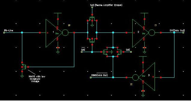
ISSN:2229-6093
                                  Sushil Bhushan et al, Int. J. Comp. Tech. Appl., Vol 2 (5), 1275-1282

         1. CELL DESIGN CONCEPT                                         and wordline2 maintained on VIdle1 and
         Fig. 1 shows a circuit equivalent to a                         VIdle2, respectively. Fig. 2 shows leakage
         developed 4T SRAM cell using supply                            current of cell for data retention when ‘1’
         voltage of 1.1V in 45nm CMOS                                   stored in cell. Most of leakage current of
         technology.                                                    access transistors is sub-threshold current
                                                                        since these transistors maintained in sub-
                                                                        threshold condition. Simulation result in
                                                                        standard 45nm technology shows if
                                                                        during idle mode of cell, BL and BLB
                                                                        maintained at VDD and GND respectively,
                                                                        and VIdle1=0.5V and VIdle2=1.1V ‘1’ stored
                                                                        in cell without refresh cycle and thus in
                                                                        idle mode above condition satisfied

             Fig. 1 New 4T SRAM cell in 45nm
                             technology
         When '0' stored in cell, load and driver
         transistor are ON and there is feedback
         between ST node and STB node,
         therefore ST node pulled to GND by
         drive transistor and STB node pulled to
         VDD by load transistor. And when '1'
         stored in cell, load and driver transistor
         are OFF and for data retention without                         Fig. 2 4T SRAM cell in idle mode when
         refresh cycle following condition must be                                 ‘1’ stored in cell
         satisfied.
            Ioff-NMOS-access ≥ 3 × (IDS-Load - IG-Driver)               Output waveform of the 4T memory cell
            Ioff-PMOS-access ≥ 3 × (IDS- Driver - IG- Load)             design is shown in the figure no.3.
         For satisfying above condition when '1'
         stored in cell, we use leakage current of
         access transistor, especially sub threshold
         current of access transistors. For this
         purpose during idle mode (when read and
         write operation don’t performed on cell)
         of cell, BL and BLB maintained at VDD
         and GND, respectively and word-line1

IJCTA | SPT-OCT 2011                                                                                           1276
Available online@www.ijcta.com
ISSN:2229-6093
Sushil Bhushan et al, Int. J. Comp. Tech. Appl., Vol 2 (5), 1275-1282
Fig.3 Output waveform of the 4T memory
cell design. Fig. 4 6T SRAM cell in idle mode when
The conventional 6T SRAM memory cell ‘1’ stored in cell
is composed of two cross-coupled CMOS 2. WRITE AND READ OPERATION
inverters with two pass transistors When a write operation is issued the
connected to complementary bit-lines [7]. memory cell will go through the
Fig. 4 shows this well known architecture, following steps.
where the access transistors AXR and 1) Bit-line driving: For a write,
AXL are connected to the word-line (WL) complement of data placed on BLB,
to perform the access write and read and then word-line1 asserted to VDD,
operations thought the column bit-lines but voltages on word-line2 and BL
(BL and BLB). All transistors have maintained at idle mode (Vword-
minimum length (Lmin), while their line2=VIdle2 and VBL=VDD ).
width is a design parameter. The value of 2) Cell flipping: this step includes two
WP defines all PMOS transistors width states as follows.
and WN defines the NMOS driver (a) complement of data is zero: in this
transistors width, while WAX the width state, STB node pulled down to GND
of the access transistors. by NMOS access transistor, and
therefore the drive transistor will be
OFF, and ST node will be floated and
then pulled p to voltage of BL (VDD)
by leakage current (most of this
current is sub-threshold current) of
IJCTA | SPT-OCT 2011 1277
Available online@www.ijcta.comISSN:2229-6093
Sushil Bhushan et al, Int. J. Comp. Tech. Appl., Vol 2 (5), 1275-1282
PMOS access transistor, and thus load ST node, power consumption is very
transistor will be OFF. small.
(b) complement of data is one: in this 4) Sensing: After word-line2
state, STB node pulled up to VDD-Vtn deactivate the sense amplifier is
by NMOS access transistor, and turned on to read data on BL. Fig. 5
therefore the drive transistor will be shows circuit schematic of sense
ON , and ST node will be pulled down amplifier that used for reading data
to GND, thus load transistor will be from new cell.
ON and STB node pulled up to VDD. 5) Idle mode: At the end of read
3) Idle mode: At the end of write operation, cell will go to idle mode
operation, cell will go to idle mode and word-line2 and BL asserted to
and word-line1 and BLB asserted to VIdle2 and VDD, respectively.
VIdle1 and GND respectively. When a
read operation is issued the memory
cell will go through the following
steps.
(a) Bit-line Pre-charging: For a read,
BL pre-charged to VDD, and then
floated. Since, in idle mode BL
maintained at VDD, this step didn’t
include any dynamic energy
consumption.
(b)Word-line activation: in this step
word-line2 asserted to GND and two
states can be considered:
Fig. 5 Circuit schematic of Sense
(1) Voltage of ST node is low: when,
amplifier
voltage of ST node is low, the voltage
of BL pulled down to low voltage by
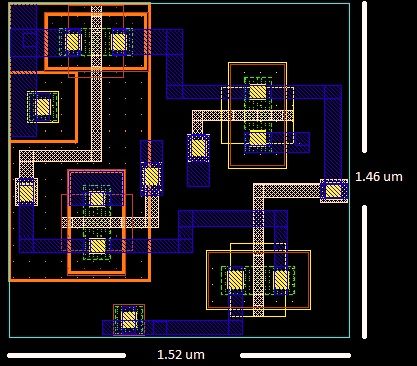
3. CELL SIZE
PMOS access transistor. We refer to
Fig. 6 shows possible layout of 6T SRAM
this voltage of BL as VBL-Low.
cell in standard 45nm CMOS technology
(2) Voltage of ST node is high: when
design rules.
voltage of ST node is high, the voltage
of BL and ST node equalized (we
refer to voltage of BL in this state as
VBL-High). Since in this state, there is
very small different between BL and
IJCTA | SPT-OCT 2011 1278
Available online@www.ijcta.comISSN:2229-6093
Sushil Bhushan et al, Int. J. Comp. Tech. Appl., Vol 2 (5), 1275-1282
Fig. 7 layout of 4T SRAM cell
4. POWER CONSUMPTION
Fig. 6 layout of 6T SRAM cell
In each cycle, a read or write operation
Also for comparison, in Fig. 7 shows
performed on one cell in SRAMs.
layout of 4T SRAM cell and 6T SRAM
Therefore dynamic energy consumption
cell in standard 45nm CMOS technology
in SRAMs consumed due to the charging
design rules. The 6T cell has the
and discharging capacitances during read
conventional layout topology and is as
and write operation, and thus during each
compact as possible. The 6T SRAM cell
cycle of SRAMs a certain amount of
requires 3.438 um2 area in 45nm
energy is drawn from the power supply
technology, whereas 4T SRAM cell
and dissipated. The power consumption
requires 2.2192um2 area in 45nm
of each cycle depended on type of
technology. These numbers do not take
operation (read or write). Furthermore,
into account the potential area reduction
when the capacitor charged from GND to
obtained by sharing with neighboring
VDD and then discharged to GND,
cells. Therefore the new cell size is
amount of energy drawn from the power
35.45% smaller than a conventional six-
supply and dissipated, equals CLVDD 2 .
transistor cell using same design rules.
And stored energy on the capacitor CL
with voltage VC equals ½ CLVC2. Thus
each time the capacitor CL charged from
VC to VDD and then discharged to VC
amount of power drawn from the power
supply and dissipated, obtained by
following expression.
Pav = [(1/T) 0 ∫T I dt] × V [1]
IJCTA | SPT-OCT 2011 1279
Available online@www.ijcta.comISSN:2229-6093
Sushil Bhushan et al, Int. J. Comp. Tech. Appl., Vol 2 (5), 1275-1282
In following power consumption of 4T Pconsumed-6T = Pav-6T-Vin - Pav-6T-Vout
and 6T SRAM cell investigated =5.682×10- 10 w = 0.5682nw
practically.
B. Power Consumption of 4T-SRAM
A. Power Consumption of 6T Cell
Conventional SRAM Cell There are four premiere capacitances in
There are four premiere capacitances in 4T SRAM cell. These capacitances
6T SRAM cell. These capacitances include BL and BLB capacitances, word
include bit-lines (BL and BLB) lines capacitances, ST capacitance and
capacitance, word-line capacitance, ST STB capacitance. BL and BLB
capacitance and STB capacitance. Bit-line capacitances are mainly composed drain
(BL and BLB) capacitance is mainly junction capacitance of access transistor
composed drain junction capacitance of of 4T SRAM cell. Next large capacitance
access transistor of 6T SRAM cell. Next in 4T SRAM cell is word-lines
large capacitance in 6T SRAM cell is capacitance and mainly composed of gate
word line capacitance and mainly capacitance of access transistors of 4T
composed of gate capacitance of access SRAM cell. And finally next capacitances
transistor of 6T SRAM cell. Next in 6T SRAM cell are ST capacitance and
capacitances in 6T SRAM cell are ST STB capacitance. These capacitances
capacitance and STB capacitance. These mainly composed drain junction
capacitances mainly composed gate capacitance of access transistors of 4T
capacitances and drain junction SRAM cell and gate capacitances and
capacitance of PMOS load transistors and drain junction capacitance of PMOS load
NMOS drive transistors of 6T SRAM transistors and NOMS drive transistors.
cell. Average power deliver by the circuit
Average power deliver by the circuit initially on the side of the Vin is
initially on the side of the Vin is Pav-4T-Vin = [(1/T) 0 ∫T I dt] × Vin [4]
Pav-6T-Vin = [(1/T) 0 ∫T I dt] × Vin [2] Here Pav-4T-vin = average power of 4T
Here Pav-6T-vin = average power of 6T from Vin supply
from Vin supply Pav-4T-Vin = 5.483×10⁻¹³ w
Pav-6T-Vin = 5.682 ×10⁻¹⁰ w Average power on the output of the
Average power on the output of the circuit is
circuit is Pav-4T-Vout = [(1/T) 0 ∫T I dt] × Vout [5]
Pav-6T-Vout = [(1/T) 0 ∫T I dt] × Vout [3] Pav-4T-Vout = 3.928 ×10 w -19
-29
Pav-6T-Vout = 7.01×10 w Power consumed by the 4T memory cell
Power consumed by the 6T memory cell is
is
IJCTA | SPT-OCT 2011 1280
Available online@www.ijcta.comISSN:2229-6093
Sushil Bhushan et al, Int. J. Comp. Tech. Appl., Vol 2 (5), 1275-1282
Pconsumed-4T = Pav-4T-Vin - Pav-4T-Vout = Because average power will be the same
5.482×10⁻¹³ w = 0.5482pw at all the values of the time constant. At
the end side of the circuit the average
C. Waveforms of 6T & 4T for power power will shown in the circuit. As per
consumption the 6T memory cell the same process
done for the 4T memory cell and the
This waveform shows the 6T memory graph is shown as fig .9.
power on the initial side of the circuit. D. Power Consumption Comparison
Cell ratio is an important parameter of
SRAM cells. This parameter defined as
the ratio of the channel width of driver
transistor of memory cell to channel
width of access transistor of memory cell
SI. SRAM Avg. Avg. Power
No. cell power on power on consumed
Vin Vout
1 6T 5.682×10- 7.01×1029w 0.5682nw
10
w
Fig. 8 Power consumption waveform of 2 4T 5.483×10- 3.928×10- 0.5482pw
13 19
6T w w
Which is connected to the Vin having [6]. As cell ratio increased also the area of
supply of 1.1V and this waveform is cell increased.
shown in the circuit which is constant
throughout the all values of the time CONCLUSION
constant. With the aim of achieving a high-density
SRAM, we developed a 4T SRAM cell.
This cell takes 35.45% less cell area with
respect to conventional 6T memory cell
and consumes less power with respect to
6T conventional memory cell. Read
operation perform from one side of cell,
and write operation perform from another
side of cell, and swing voltage reduced on
word-lines thus power during read/write
operation reduced.
Fig. 9 Power consumption waveform of
4T
IJCTA | SPT-OCT 2011 1281
Available online@www.ijcta.comISSN:2229-6093
Sushil Bhushan et al, Int. J. Comp. Tech. Appl., Vol 2 (5), 1275-1282
REFERENCES [5] A. Kotabe, K. Osada, N. Kitai, M.
[1] K. Osada, Y. Saitoh, E. Ibe, and K. Fujioka, S. Kamohara, M. Moniwa, S.
Ishibashi, “16.7-fA/cell tunnel Morita, and Y. Saitoh, “A Low-Power
leakage- suppressed 16-Mb SRAM for Four-Transistor SRAM Cell With a
handling cosmic-ray-induced multi Stacked Vertical Poly-Silicon PMOS
errors,” IEEE J. Solid-State Circuits, and a Dual-Word-Voltage Scheme,”
vol. 38, no. 11, Nov. 2003, pp. 1952– IEEE J. Solid-State Circuits, vol. 40,
1957. no. 4, April 2005, pp. 870-876.
[2] Fdf M. Yamaoka, Y. Shinozaki, N. [6] K. Noda, K. Matsui, K. Imai, K.
Maeda, Y. Shimazaki, K. Kato, S. Takeda, and N. Nakamura, “A load
Shimada, K. Yanagisawa, and K. less CMOS four-transistor SRAM cell
Osada, “A 300-MHz, 25 A /M bit in a 0.18- logic technology,” IEEE
leakage on-chip SRAM module Trans. Electron. Devices, vol. 48, no.
featuring process-variation immunity 12, Dec. 2001, pp. 2851–2855.
and low-leakage-active mode for [7] G. Torrens, et al. 2008. Analysis of
mobile-phone application processor,” Radiation Hardening Techniques for
in IEEE Int. Solid-State Circuits Conf. 6T SRAM with Structured Layout.
Dig. Tech. Papers, Feb. 2004, pp. IEEE Int. Reliability Physics Sym.
494–495.
[3] K. Ishibashi, K. Takasugi, K. Komi-
yaji, H. Toyoshima, T. Yamanaka, A.
Fukami, N. Hashimoto, N. Ohki, A.
Shimizu, T. Hashimoto, T. Nagano,
and T. Nishida, “A 6-ns 4-Mb CMOS
SRAM with offset-voltage insensitive
current sense amplifiers,” IEEE J.
Solid-State Circuits, vol. 30, no. 4,
Apr. 1995, pp. 480–486.
[4] T. Yamanaka, T. Hashimoto, N. Ha-
segawa, T. Tanaka, N. Hashimoto, A.
shimizu, N. Ohki, K. Ishibashi, K.
Sasaki, T. Nishida, T. Mine, E.
Takeda, AND T. Nagano, “Advanced
TFT SRAM cell technology using a
phase-shift lithography,” IEEE Trans.
Electron. Devices, vol. 42, no. 7, Jul.
1995, pp. 1305–1313.
IJCTA | SPT-OCT 2011 1282
Available online@www.ijcta.comYou can also read