Recon gurable Antennas: A Review of Recent Progress and Future Prospects for Next Generation
←
→
Page content transcription
If your browser does not render page correctly, please read the page content below
Progress In Electromagnetics Research, Vol. 171, 89–121, 2021

 Reconfigurable Antennas: A Review of Recent Progress and Future
                  Prospects for Next Generation

               Ryan J. Beneck* , Arkaprovo Das, Galestan Mackertich-Sengerdy,
               Ryan J. Chaky, Yuhao Wu, Saber Soltani, and Douglas H. Werner

                                                    (Invited Paper)

Abstract—Reconfigurable antennas are devices that can dynamically alter their geometry and/or
electromagnetic properties to facilitate different behaviors. Numerous approaches for achieving
reconfigurability have been studied over the past 20 years, mainly consisting of mechanical, electrical,
optical, and metamaterial methods. This review presents the most notable works and advancements in
this field while placing a significant focus on antennas with explicit practical applications in the emerging
areas of millimeter waves, 5G/6G communications, Internet-of-Things (IoT), high-throughput satellites,
and miniaturized systems among several others. The various reconfiguration methods mentioned will
be compared, and their benefits and drawbacks discussed.

1. INTRODUCTION

The broad subject of Reconfigurable Systems [1–6] has garnered significant attention over the last few
decades and has been a topic of active research in the recent past. Reconfigurable antennas [7] constitute
an extensive segment of reconfigurable systems aimed at achieving reconfigurability primarily at the
RF, microwave and millimeter-wave regimes of the frequency spectrum. With technology trends and
applications such as 5G communications, Internet-of-Things (IoT), autonomous vehicles, integrated
space and terrestrial networks gaining prominence, the need for developing novel and cutting-edge
design technologies to achieve reconfigurability in antenna systems is even more necessitated. This
review article is directed towards furnishing the readers with a perspective of recent advancements
in the field of reconfigurable antennas, the technological innovations that demonstrate reconfigurable
characteristics, the latest growth trends and traction in this discipline and the authors’ standpoint on
futuristic prospects of technologies that could be implemented into commercialized applications. It is
noteworthy that there have been several review papers published previously on reconfigurable antennas.
However, a significant number of new and innovative developments have been reported since these papers
first appeared. This review article therefore focuses mainly on providing a summary of significant recent
developments in the field as well as some insights into the future prospects for next generation systems.
      Reconfigurable antennas are antennas or an array of antenna elements that can dynamically
achieve a reversible alteration of operating frequency, radiation-pattern properties, polarization modes,
bandwidth characteristics or a combination of a few or all of these aspects to suit a specific application.
These antennas have a major advantage of being multi-functional in nature, which subsequently reduces
the number of antennas required and hence the total occupied footprint for performing multiple specific
objectives. Frequency reconfigurable antennas can dynamically tune-in to different frequencies of
  Received 11 August 2021, Accepted 11 October 2021, Scheduled 16 October 2021
* Corresponding author: Ryan J. Beneck (rbeneck95@gmail.com).
The authors are with the Computational Electromagnetics and Antennas Research Laboratory (CEARL) at The Pennsylvania State
University, USA.
90                                                                                           Beneck et al.

operation, thereby alleviating the need to design multi-band antenna systems. Pattern reconfigurable
antennas can steer the main radiation beam, place nulls at intended angular locations, and alter the
pattern shape, directivity, and gain of the antennas depending on the applications they cater to.
This contrasts with the smart and adaptive antenna technology where the adaptive beam switching
operation is largely dependent on an external beam-forming network instead of an internally equipped
tuning mechanism. Polarization reconfigurable antennas on the other hand can switch between different
polarization states, for example — switch from a vertically polarized pattern to a circularly polarized
one. This multi-functional trait of reconfigurable antennas has attracted a lot of interest over the last
few years. Figure 1 shows the growth in the number of technical articles published in IEEE journals
and conference proceedings since 2000.

                          2500

                          2000

                          1500

                          1000

                            50

                             0
                                 2001-2004 2005-2008 2009-2012 2013-2016 2017-2020

Figure 1. Bar chart representing the growth of IEEE publications related to “Reconfigurable Antennas”
over the last 20 years.

      Reconfigurability in an antenna system is generally achieved by dynamically modifying the path
traversed by the currents on the structure or by changing the antenna’s effective aperture. Additionally,
for an array of antenna elements, this is traditionally accomplished by customizing the amplitude and
phase excitations of the individual radiators. There are a plethora of techniques described in the
literature that aid in realizing the aforementioned objectives. The most popular electrical approach
among them is to incorporate RF micro-electromechanical systems (MEMS) and active switches in
the antenna design configuration [8–11], which subsequently generates a dynamic switching response
to effectively change the current distribution. Recently, artificially engineered materials such as
metamaterials and metasurfaces have been demonstrated to be effective in obtaining reconfigurable
and tunable characteristics for antenna applications [2]. Alternatively, switching mechanism can also
be triggered by invoking optically induced phenomena such as photoconductive effects [12], Optically
Induced Plasmas (OIP), etc. Furthermore, mechanical reconfigurability of several parts of the antenna
system can also result in tunable electrical characteristics [7]. Figure 2 depicts different methods and
technologies used for achieving antenna reconfiguration. The work is broadly classified into 4 sub-
categories: mechanical, electrical, optical and metamaterial methods.
      The remainder of the paper describes each of the reconfiguration methods in further detail. Section 2
highlights the mechanical methods that have been employed for reconfiguration. Although not sorted
according to priority, mechanical methods being the oldest option have been placed on the top of the list.
Section 3 enumerates the pros and cons of several electrical technologies to achieve reconfiguration, while
optically induced reconfiguration mechanisms are explained in Section 4. Section 5 outlines the role of
artificially engineered materials such as metamaterials, metasurfaces and frequency selective surfaces
in obtaining reconfigurable characteristics, with emphasis on space and next generation terrestrial
applications. Section 6 concludes the paper with notes on future prospects.

2. MECHANICAL METHODS

One of the first reconfigurable antennas consisted of the integration of mechanical components into
the antenna’s operation. In 1935 a rhombic antenna radiation pattern was altered by adjusting
Progress In Electromagnetics Research, Vol. 171, 2021                                                                             91

                                  Varactors
                                                                                               Laser Diodes
                                    MEMS
                                                                                         Integrated Optical Fibres
                         Diode and Transistor Switches
                                                                                         Photoconductive Switches
                                                 Electrical
                                                                               Optical

          Conductivity
     Phase Change Materials
        Resistive Memory
         Reconfigurable
     Permittivity/Permeability

                                  Material
                                                              Reconfigurable
                                                                 Antenna
                                                               Technology

                                                                               Metamaterial
                                                                                              Frequency Selective Surfaces
            Gears, Linkages, Pulleys
                    Origami
                                          Mechanical                                              Transparent Surfaces
               Flexible Materials                                                                  Foldable Structures
                    Fluidics                                                                Reconfigurable Intelligent Surfaces
             Shape Memory Alloys

Figure 2. Visual summary of the broad classification of different methods to achieve reconfiguration.

counterweights changing the inclusion angle of the wire elements [13]. One of the most famous
applications of mechanical methods is the Gregorian dome and carriage house of the Aricebo
observatory [7]. Recently, there have been advancements in the mechanical methods such as the
implementation of dielectric fluid loaded antennas, conductive fluid antennas, gearing and linkage
systems, and origami-based antennas.
     Some of the most popular mechanical based antennas are the gear/linkage-based systems. These
are antennas or antenna systems that consist of a rotating/translating layer that can alter the operating
frequency [14, 15], steer the resultant beam to the desired direction [16–19], create ultrawideband or
stopband frequency operation [20] or change the resultant polarization [21, 22]. Another method to
introduce reconfiguration can be achieved by implementing origami techniques. Origami (the art
of paper folding) has similar reconfiguration capabilities such as the polarization and/or frequency
reconfiguration [23, 24]. However, utilizing the art of origami, antennas can be stored or transported
as flat sheets (reducing total package size) and when they reach their application destination, are
folded/unfolded into the operational shape [25, 26]. The shape modification for reconfiguration is not
limited to strictly origami methods. The lamination of asymmetric glass fibers into the substrate and
activating springs fabricated from Ni/Ti shape memory causes the substrate to deform into 2 differing
shapes. This mechanical reconfiguration method allows the resultant beam to be steered to two differing
angles [27]. Figure 3 shows an origami segmented helix antenna with reconfigurable polarization.
     An interesting application of a mechanically reconfigurable antenna is the high gain slotted
waveguide with a simple rotating shutter system for 5G applications (shown in Figure 4). It
demonstrates that even at the higher 5G frequencies a robust and simple mechanical solution is
achievable.
     Some of the more interesting applications of mechanical based reconfiguration methods are their
implementation into high-power systems. As presented by Campbell et al., mechanical methods used
with a 2D unit-cell and then later a 3D unit-cell (shown in Figure 5) can achieve a target reflection phase
angle behavior under high power microwave conditions [28]. This solution was then demonstrated by the
successful completion of a fabricated prototype [29]. Some other mechanical reconfiguration methods
applied to high power applications involve the modification of the half-power beamwidth (HPBW) of a
horn antenna by changing the location of metal flaps [30]. This method was successful in changing the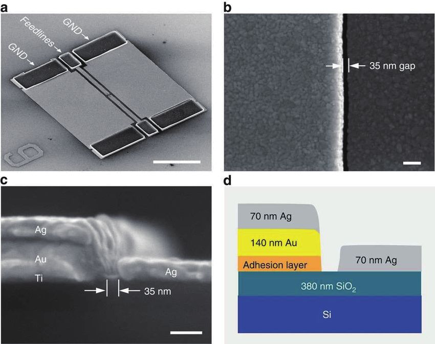
92                                                                                          Beneck et al.

                                     (a)                           (b)

Figure 3. Segmented helix antenna fabricated using origami methods. (a) Left-handed state. (b)
Right-handed state. ⃝
                    c 2018 IEEE. Reprinted, with permission, from [23].

                               (a)                                   (b)

Figure 4. (a) Omnidirectional ring based slotted waveguide array as fabricated. (b) Radiation pattern
mechanically configured array at 27.3 GHz with 17.4 dBi of realized gain. ⃝ c 2017 IEEE. Reprinted,
with permission, from [17].

HPBW from 58.7 to 16.5 degrees.
     Fluidic devices are another interesting class of antennas that achieve reconfigurability by adjusting
the fluid level within a device to create a reconfigurable resonant chamber. This is done by either
adjusting the fluid composition and channels, or by having shaped fluid filled containers to achieve
novel performance. These antennas can use pure water, sea water, ionic liquids, room-temperature
liquid metals, colloidal dispersions in dielectric oils or various other liquids [3, 31–37].
     The mechanical methods that are described above are just a small sub-set of all the existing
mechanical methods used for reconfiguration. There are several other mechanical methods that are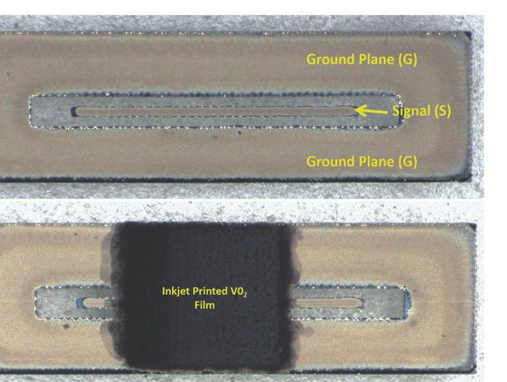
Progress In Electromagnetics Research, Vol. 171, 2021                                                  93

                            (a)                                                   (b)

Figure 5. (a) Fabricated and assembled mechanically reconfigurable metamaterial enabled high power
antenna. (b) Simulated and measured far-field gain patterns for broadside and steered configurations.
⃝c 2020 IEEE. Reprinted, with permission, from [29].

available for 5G and future communication applications. These include physically deforming the
parabolic reflector surface using flexible materials and liquid-metals to stretch and fold the antenna
to achieve reconfiguration, and textile-based antennas that are frequency reconfigurable [38–40].

3. ELECTRICAL METHODS

The electrical techniques used for actuating reconfiguration in antennas are broadly dependent on
effective switching mechanisms. This can be realized either by using electronic and mechanical switches
such as PIN diodes, MEMS switches, etc. or by effectively altering the constituent properties of
materials. Subsections 3.1–3.3 illustrate several electronic and electro-mechanical switches used for
the purpose. On the other hand, the use of material properties for achieving reconfiguration is detailed
in Subsections 3.4–3.7.

3.1. Conventional Diode and Transistor Switches
The most common electronic switching technique is the usage of PIN diodes due to its affordability,
excellent power handling capability, scalability, prolonged lifetime, simple control, compactness, ease of
fabrication for optimal results, higher switching speed in the orders of nanoseconds, and reliability [41–
43]. As the control current is varied between the HIGH and LOW states, these diodes facilitate switching,
pulse modulation, phase shift and attenuation of the radio frequency signals [44]. However, the PIN
switches suffer from a few disadvantages due to their non-linearity, lower isolation, high power losses
and high insertion losses [41–43]. The insertion loss in these switches was found to be in between 0.4
and 0.7 dB [45]. With increasing number of PIN diodes in the system, the biasing circuitry becomes
increasingly complicated, and the insertion loss considerably increases [45].
     On the other hand, GaAs FET switches exhibit higher switching speeds, better isolation properties,
lesser insertion losses, compact sizes, lower power consumption, easier integration with the antenna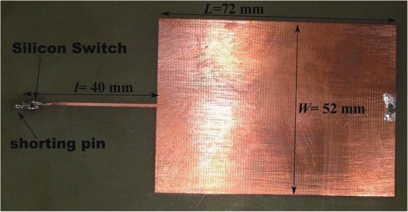
94                                                                                          Beneck et al.

systems, lower assembly cost and low ON state resistances [43]. FET switches, unlike PIN diodes, do
not need RF chokes in their biasing networks. As the biasing technique is simpler, the FET switches
exhibit no adverse effects in the pattern, gain and efficiency of the antenna. CMOS switches exhibit
high power handling capabilities, easier integration into the antenna design and easier control. Even for
higher voltage amplitudes, the CMOS switches exhibit a linear response. However, a smaller number of
tuning states can only be realized with these switches [46]. Figure 6 depicts the top and bottom views
of a reconfigurable antenna for 2.5 GHz operation. Here the reconfiguration is affected by using PIN
diodes as switches. Recently, many reconfigurable antennas using PIN diodes as switches have been
reported for frequency [47, 48], pattern [48–51], and polarization [48, 51] reconfiguration.

                                     (a)                                (b)

Figure 6. Reconfigurable antenna for 2.5 GHz operation: (a) Photograph of the top view. Inset: switch
structure. (b) Photograph of the bottom view. Inset: dc bias lines. ⃝c 2017 IEEE. Reprinted, with
permission, from [46].

3.2. Varactor Switches and Tuned Capacitances
Varactors are voltage-controlled capacitors with fast switching speeds and can be easily integrated into
antenna circuitry due to their smaller sizes [42, 52]. Varactors are used for fast and easier tuning and
provide a broader tuning range [52]. These devices are compact, readily available commercially, and low-
priced. As varactor diode switches are operated using reverse bias voltages, a lower current consumption
is required as compared to PIN and MEMS switches for their activation, thus resulting in lower power
consumption [53]. A minimum number of varactor switches can provide multiple modes with more
flexibility [53]. On the flip side, the use of varactors for reconfiguration purposes is hindered by their
nonlinear response and high voltage requirements [42]. Figure 7 below shows the use of varactor diodes
in conjunction with a metasurface-based Artificial Magnetic Conductor (AMC) to miniaturize a planar
crossed end-loaded dipole (ELD) antenna [54, 55]. This strategy enables the operation of the tuned
antenna over a frequency range of one to two octaves as well as facilitates a reconfigurable polarization.
     In a similar context, there has been a substantial amount of literature that refers to the use of
switchable capacitances for achieving reconfigurability. This is traditionally attained by using lumped
capacitor components, while other methods of generating the capacitance values are also reported.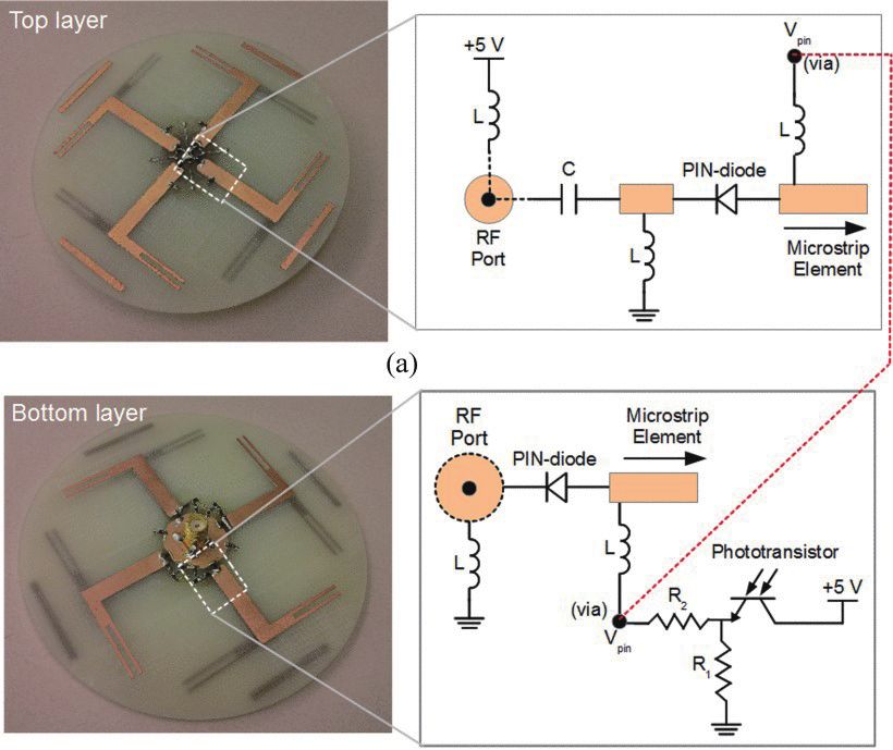
Progress In Electromagnetics Research, Vol. 171, 2021                                               95

                                                 (a)

                                                 (b)

Figure 7. Antenna geometry and photographs. (a) Side-view schematic of the antenna. The thickness
from the ground plane to the ELDs is 4 cm, while the total antenna thickness approaches 4.5 cm when
including circuit components on both the top and bottom circuit boards. (b) Photographs showing the
details of antenna and the tunable AMC. ⃝ c 2016 IEEE. Reprinted, with permission, from [54].

It is noteworthy to mention that the use of switchable capacitances can accomplish reconfigurability
for both resonant and leaky-wave antennas (LWA). LWAs are antennas that leak radiation from the
structure when a guided-wave mode propagates through them. This property of LWAs enables beam-
steering capabilities as the frequency is varied. Although the steering angle of the main lobe depends
on the propagation constant of the propagating mode, β, a lack of control of the main beam can still
stem from the non-linear dependence of β on frequency due to dispersion. Furthermore, for band-
limited systems, the maximum allowable frequency bandwidth might be restricted while the scanning
coverage desired is wider. In those cases, dependence on frequency of operation to achieve beam-
steering capabilities can severely hinder the scan coverage of the antenna. These factors necessitate
the need for developing LWAs equipped with a potential for reconfiguration that can steer the main-
beam at a fixed frequency of interest, a technique also known as ‘fixed-frequency beam scanning’. It
has been shown in [56] that the propagation constant β can also be altered at a fixed frequency by
changing the admittance of the radiating wall of the LWA. Exploiting this property, the work in [57]
proposes genetic-algorithm optimized switch configurations that optimally switch between 35 equally-
spaced 0.2 pF capacitors loading a reconfigurable half-width microstrip LWA to achieve beam-steering.
Suntives and Hum in [58, 59] make use of a series-shunt configuration of lumped capacitors to alter the
wall admittance of the LWA. Deviating from the usage of traditional passive lumped elements, the recent
work in [60] uses a PIN-diode to switch ON/OFF two gap-coupled capacitances loading a half-width
microstrip LWA. This double-gap capacitor technique enabled the antenna prototype to scan the main
beam forward between +28◦ and +67◦ and backward between −27◦ and −66◦ at 4.2 GHz.
96                                                                                         Beneck et al.

3.3. MEMS Switches
MEMS switches are traditionally limited in terms of packaging, reliability and power handling
capabilities [8, 9]. These switches exhibit a slower response and a lower tunable range as compared to
their PIN diode and varactor counterparts. Whereas, compared to the discrete components’ integration
into the antenna design, monolithic fabrication of antenna and switches together minimizes the losses
and parasitic effects [41]. Furthermore, MEMS switches require complex matching networks [42].
They also need additional voltage upconverter chips of 30 to 90 V conversion levels if used in portable
communication devices. The process of assembling these switches into Printed Circuit Boards (PCBs)
is reportedly difficult. The requirement of higher voltages for activation is another disadvantage of
MEMS switches which makes them less reliable for practical use [41–43]. In [10], a parasitic layer-based
multifunctional reconfigurable antenna (MRA) with an interconnecting MEMS switch is presented,
as shown in Figure 8. The antenna tunes its operating polarization/radiation pattern according to
switch combinations. In recent years, examples of reconfigurable spiral-shaped monopole antennas [61],
concentric ring structured reconfigurable antennas [62] and frequency reconfigurable antennas [63] using
MEMS switches have also been demonstrated.

Figure 8. Three-dimensional schematic of the “MRA parasitic” with a magnified view of adjacent pixels
and an interconnecting MEMS switch (for the sake of illustration, the parasitic layer is suspended on
top of the patch layer). ⃝
                         c 2012 IEEE. Reprinted, with permission, from [10].

     In general, the installation of electrical switching components within antenna structures increases
the circuit intricacies and enhanced losses since these switches use biasing connections for activation.
This phenomenon adversely affects the radiation pattern of the antenna [42]. In this context, it is
noteworthy to explain some designs which are least affected by the above mentioned issues. In many
recently reported works, DC bias lines are not required for several novel geometries that employ MEMS
switches. This results in easier fabrication and improved radiation patterns as any leakage loss or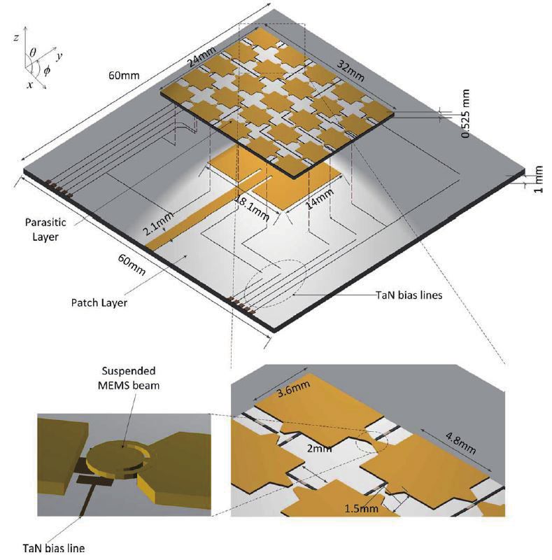
Progress In Electromagnetics Research, Vol. 171, 2021                                                 97

coupling loss with the bias lines can be readily mitigated. In some designs, the biasing circuit is
integrated into the antenna plane for PIN diodes without any vias, which in turn reduces the losses
associated with bias lines [11]. FET switches can also be activated by a digital signal without requiring
a DC bias or biasing networks as reported in [43].

3.4. Resistive Memory and Memristors
Memristors and resistive memory devices can change their resistances based on external stimuli [64, 65].
Notably, they are both passive and require no additional energy to maintain a resistance state once
reached [66]. Memristors are sometimes combined with other circuit elements and can be used in the
design of tunable filters which are commonly implemented to switch between band-pass and band-stop
modes. The operation of these filters in band-pass mode allows a signal to be better received in low
noise situations, while band-stop mode eliminates unnecessary signals in noisy environments. These
filters are therefore a popular choice for use in 5G applications. Although tunable filters predominantly
consist of conventional active devices such as transistors, relays, PIN diodes, or MEMS, the use of
memristors for this purpose consumes less energy and has better performance potential compared to
traditional devices [67, 68]. Two examples of reconfigurable devices that incorporate memristors are
shown in Figure 9 below.

                      (a)                                                     (b)

Figure 9. (a) Diagram of a memristor-enabled reconfigurable band-switching antenna. (b) Diagram
of a polarization reconfigurable patch antenna containing memristors. ⃝
                                                                      c 2015 IEEE. Reprinted, with
permission, from [65].

     A simulated tunable filter consisting of a memristor, varactors, and a stub-loaded stepped-
impedance resonator is presented in [69]. A tuning range from 3.4 GHz to 3.6 GHz was achieved,
which fits into one of the mid-band 5G spectra. This design was not fabricated, and a material
for the memristor was not chosen. However, the authors see great potential in this setup for use in
future 5G systems. Nevertheless, memristive switches are not only limited to this frequency range. As
reported in [70], nanoscale memristive switches have demonstrated operation from 10 GHz to 40 GHz.
This nanoscale design was fabricated on a silicon wafer with thermally grown silicon dioxide. Other
materials used in construction were gold, titanium, and silver. This device’s frequency range includes
many millimeter wave bands of the 5G spectrum, and the researchers emphasize that this technology
will likely become prominent in future consumer electronics and RF circuit applications. An example
of one of these nanoscale switches is shown in Figure 10 below.
     Another form of resistive memory switch derives from 2D materials and is known as an atomristor.
2D materials, such as graphene and h-BN (hexagonal boron-nitride) are structures which are a single
atom in thickness and have useful material properties. Many of these 2D materials have been shown to
have non-volatile resistance switching (NVRS) properties. The works in [71] and [72] show examples of
atomristor RF switches which are operational up to 50 GHz and 100 GHz respectively, and thus includes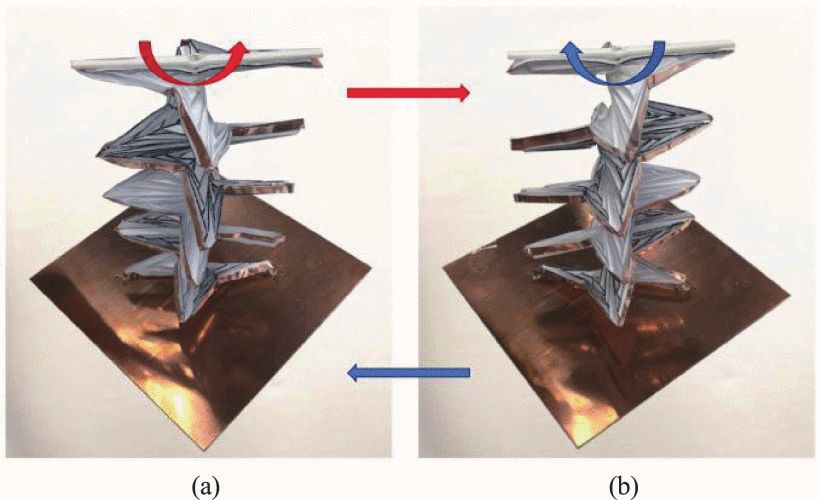
98                                                                                          Beneck et al.

                                 (a)                                   (b)

                                 (c)                                   (d)

Figure 10. (a) Nanoscale memristive RF switch. (b) Top view of air gap. (c) Cross-sectional
view of air gap and electrodes. (d) Diagram showing geometry of the device and the materials used.
Reprinted by permission from Springer Nature Customer Service Centre GmbH: Springer Nature, Nature
Communications [70] ⃝ c 2015.

several bands in the 5G millimeter wave spectrum.
     Resistive memory-based RF switches have potential for use in future 5G and X-band systems. This
newer technology has numerous performance benefits over older devices. While these switches are yet to
become commonplace, many researchers in this field see the potential of resistive memory as important
components of future 5G and X-band reconfigurable antennas.

3.5. Phase Change Materials (PCM)
In the past two decades, various research groups have focused on developing multifunctional RF devices.
Phase Change Materials (PCMs), which provide an extra freedom of tunability, have become an
inevitable choice besides the more conventional temporal and spatial modification techniques. PCMs
have been used to design devices for X-band applications rather than 5G. One example presents a
reconfigurable bandpass filter with an uplink frequency range of 7.9–8.4 GHz and a downlink range of
7.25–7.75 GHz [73]. However, it does suffer from issues of reliability and robustness. A second example
demonstrates a laser-excited RF switch [74]. As a third example, PCM based switches have been utilized
in coupled microstrip lines to achieve similar functionality [73]. In these three cases, the phase change
material used is Germanium telluride (GeTe).
     Vanadium dioxide (VO2 ) is a popular phase changing material capable of going through a fast and
reversible phase transition. At a critical temperature of 341 K, it can transition from a semi-conductor
to a metallic state. The change in optical properties in PCMs is accentuated by the transition between
two crystalline states — the monoclinic structure below the critical temperature and the tetragonal
structure above the critical temperature. By taking advantage of the fast response speed of the PCM,
high frequency RF, millimeter wave and photonic devices have been proposed with dual or even multiple
functionalities. In [75], a laser deposited VO2 based reversible RF-microwave switch was experimentally
Progress In Electromagnetics Research, Vol. 171, 2021 99
proven by researchers, which has a potential for use in various tunable high frequency communication
devices. The switches were investigated with both shunt and series configurations, which proved to
have 30–40 dB isolation from 500 MHz to 35 GHz and a 2.5 dB loss when operating in the ON-state. In
2014 [76], a single-pole single-throw (SPST) VO2 based millimeter wave switch was proposed with low
insertion loss (0.2 dB in the ON-state) and high isolation (21 dB in the OFF-state). The device reached
a 40 THz cut-off frequency with a low off-capacitance of 4 fF and a low power budget (2 V, 8 mA), which
enables high-performance millimeter FPGA operation. In 2015, a low loss (0.13 dB at 50 GHz, 0.5 dB at
110 GHz) VO2 millimeter wave switch with a 45 THz cut-off frequency was proposed, which can operate
up to the W-band spectrum [77]. The same group also reported an SPST configured series switch that
has < 1 dB insertion loss and > 12 dB isolation at 220 GHz, which is suitable for millimeter and sub-
millimeter wave applications [78]. Another notable work combined a thin VO2 film with a nanoscale
metal resonator to create a versatile multifunctional platform capable of computer control [79]. This
approach can serve as a basis for creating future reconfigurable intelligent nanophotonic systems. As a
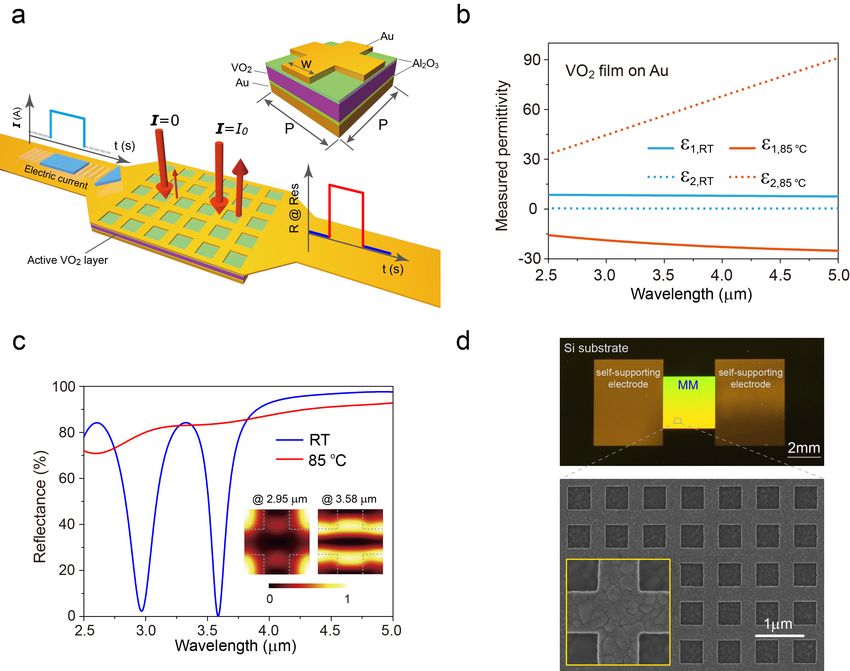
proof of concept, the researchers used this method to create a hybrid metamaterial absorber (Figure 11)
and for infrared camouflage. In [80–82], researchers demonstrated for the first time a VO2 -ink-printed,
thermally controlled reconfigurable mechanism on a custom silver-organo-complex (SOC) ink supported
flexible Kapton substrate, which was experimentally validated using antenna and switch configurations
(PIFA, CPW switch) for different frequency ranges (Figure 12 shown below).
(a) (b)
(c) (d)
Figure 11. (a) Diagram of metamaterial absorber with gold (Au) and VO2 layers. (b) Permittivity
of VO2 at different temperatures. (c) Simulated Reflectance of the absorber. (d) Photo of
the absorber from an electron microscope. [79] ⃝ c Liu et al. 2016, licensed under CC BY 4.0.
http://creativecommons.org/licenses/by/4.0/.100 Beneck et al.
(a) (b)
(c) (d)
Figure 12. (a) Photo of fabricated series and shunt switches on Sapphire wafer. (b) Microscopic images
of inkjet-printed CPW structure for shunt switches and inkjet-printed VO2 film on top of printed CPW
structure. (c) Fabricated prototype of the VO2 -based PIFA antenna. (d) The measured reflection
coefficient of the antenna with the VO2 switches in the ON/OFF state in flat condition. Adapted
from [81] ⃝c 2018 WILEY-VCH Verlag GmbH & Co. KGaA, Weinheim.
Another class of PCMs that recently attracted tremendous attention in the RF community is
chalcogenides, such as GeTe (Germanium Telluride), and GeSbTe (Germanium-Antimony-Tellurium or
GST). The tunability of this class of PCM is induced by the transition between the crystalline state and
the amorphous state, either electrically or thermally. Similar to VO2 , these materials also demonstrate
a critical temperature, on either side of which they exhibit a significant change in their electromagnetic
properties. These PCMs are widely implemented in photonic devices. A GeTe reconfigurable RF switch
was achieved with low ON resistance (180 Ohms) and large dynamic range (over 7000 times) [83] under
a 5 ns rise time for the electrical pulse excitation. In [84–86], a three-terminal and a 7 THz-cutoff four-
terminal topology for the RF switches were exploited to realize a high OFF/ON resistance contrast,
50 Ohm/3.5 kOhm and 1.2 Ohm/113 kOhm, respectively. In these two configurations, the phase change
from a conductive crystalline state to a high resistance amorphous state is induced by an external
current (∼ 10 mA) and an external voltage pulse modulation. In [87], a 12.5 THz cut-off inline phase
change switch (IPCS) is realized with two configurations — single-pole single-throw (SPST) and single-
pole double-throw (SPDT). The proposed IPCSs are designed with a significantly low on-resistance
(0.9 Ohm) and off-capacitance (14.1 fF), which cumulatively contribute to a high cut-off frequency.
Meanwhile, in addition to the ON/OFF state resistances as described above, some researchersProgress In Electromagnetics Research, Vol. 171, 2021 101
have emphasized different Figures of Merit (FoM) including but not limited to thermal budget,
response speed, stability, 1 dB compression point, etc. In [88], researchers modeled and experimentally
characterized the critical RF and thermal specifications such as Joule’s heating simulation, third order
intercept point, response speed and 1 dB compression point (P1 dB) of the GeTe based RF switches.
They reported a crystallization switch of 20 µs and an amorphous switch of 500 ns, while the P1 dB
of the switch was around 20 dBm, which provides a superior performance to traditional MEMS-based
switches in terms of switching speed and integration density. Another characterization of the GeTe
based RF active elements was conducted in [89], where the optimized device was demonstrated to
have a wideband low resistance (1.8 Ohm) in the ON-state and a low-profile of 300 nm thickness. In
general, the device is capable of a large OFF/ON contrast of 1.8 × 10⁴ with a 0.2 dB insertion loss up-to
40 GHz. Moreover, the GeTe switches were first fabricated with a lateral FET configuration in series
and shunt fashion [90, 91]. This switch also has an insertion loss of < 0.2 dB and an isolation of 30 dB
up to 67 GHz. A GeTe RF switch for operation at 11 THz was designed and tested under W-CDMA
signals. An insertion loss of 0.25 dB and an isolation of 24 dB was reported with a 50-µm-wide device
at 20 GHz [92]. A thermal stability analysis and the dependence of ON-state power handling capability
of GeTe RF switches on the number of conditioning cycles has been studied in [73]. It has been shown
that the power handling of a GeTe switch, thermally actuated by a tungsten heating mechanism can
be increased by ∼ 2 dB if the device is continually cycled over time for a few cycles. Furthermore, a
low power budget GeTe based RF switch was designed with a CMOS integration process, which has a
cut-off frequency of 22 THz and performs up to 65 GHz with large on-off contrast [93]. In 2018, SbTe
was introduced as a new chalcogenide material, and the alloy was utilized in the construction of an RF
switch. It was then fabricated on a TiW (Titanium Tungsten) heater substrate in a planar configuration,
and this setup yielded a high FoM [94].
3.6. Reconfigurable Permittivity and Permeability Materials
Dynamic adjustments in the permittivity and/or permeability of a material alter the effective electrical
dimensions (e.g., length) of an electromagnetic structure such as an antenna, which results in a shift
in the frequency of operation [4]. This concept has been predominantly used to design reconfigurable
antennas. There are different types of materials that can be used for this purpose and depending on
the choice; a different stimulus or method is needed to modify their constituent properties.
Ferroelectric (FE) materials, with high dielectric constant and large tunability are widely utilized in
the design of memory, sensors, actuators, and MEMS devices. The electromagnetic reconfigurability in
FE materials stems from the external biasing field, the application of which can change the constitutive
parameters. Due to their smaller footprint and low power budget, planar RF applications with FE
composites, such as FE antennas [95], have been proposed over the past two decades. Furthermore,
some FE materials with oxide doping, e.g., PSTO (lead strontium titanate oxide) and BSTO (barium
strontium titanate oxide), maintain a relatively high dielectric constant while suppressing the loss
tangent, which makes them even more suitable for high frequency RF applications. In 2001 [95],
researchers first realized a 2D beam scanning capability across 20–60 GHz by integrating the low-loss
ferroelectric material, BSTO, into the circularly arranged transverse stub design (CTS). The material
that was chosen had a low loss tangent of 0.0009 and a high dielectric contrast (permittivity) tuning
range of 19.81% (416.4–333.91). Another ferroelectric based single frequency scanning LWA [96] was
proposed based on the transverse equivalent networks model, where the conductive superstrate of a
slot array was used as both the partial reflective plane and the biased electrode. A screen-printed
barium-strontium-titanate (BST) based phase-shifter antenna array operating at 10 GHz was designed
with 100◦ of scanning range and a relatively high FoM [97]. By integrating a tunable BST layer,
researchers realized a shifter configured for left-handed operation and associated bias circuitry with a
fully planar configuration while not sacrificing the high FoM, > 52◦ /dB. Similarly, a compact screen-
printed BST RF phase shifter was demonstrated with a high FoM of 45◦ /dB and a large phase shift range
of 330◦ from 8.5 GHz to 13 GHz, which also makes use of the left-handed configuration [98]. In recent
years, alternative FE materials have been investigated. In 2021, Aspe et al. implemented interdigitated
varactors based on K0.5 Na0.5 NbO3 material to create a frequency-tunable slot-loop antenna [99]. There
has also been interest in the FE material lead magnesium niobate — lead titante for use in reconfigurable
systems [100].102 Beneck et al.
Liquid Crystal (LC) [5] is another good candidate for reconfigurable antenna technology due to its
ability to tune the dielectric constant of the material [101]. A 3%–30% [102–104] permittivity variation
ratio at different frequency ranges has been achieved by using LC. Also, LCs can be tuned thermally
and electrically between all their various crystal phases. Previously, the potential of LC to realize
reconfigurable devices has been investigated only in the optical region [105–109]. Its usage is more
preferable at higher frequencies, predominantly over 30 GHz, because of its lower loss tangent, which
makes it more competitive for 5G or millimeter-wave applications. In [110], a 5 GHz microstrip antenna
with an LC substrate was proposed with a tri-layer Taconic TLY-5 substrate architecture. It realizes an
impedance matching and broadside radiation performance from 5.75 GHz at 0 V bias to 5.3 GHz at 10 V
bias, resulting in an 8% tunability range. In 2015, an LC based reconfigurable reflectarray antenna with
a beam scanning range of 55◦ at 96–104 GHz was proposed that achieved a side lobe level of −13 dB
across the angular range [111]. A novel shape-memory-polymer, liquid crystal elastomer (LCE), was
used as an antenna substrate to enable tunability under a temperature change [112]. A k15 LC substrate
antenna was compared with a conventional RT/Duroid 5880 substrate antenna, which outperforms the
conventional counterpart with a bandwidth of 6.43%, a tuning range of 3.1% and a peak radiation
efficiency of 70% [113]. In 2018, a differential probe-fed LC based frequency tunable circular ring patch
antenna was proposed [114], in which the cavity model was utilized to analyze the differential operation
and extract the permittivity of the tunable substrate.
LCs can also be used in reconfigurable LWAs [115]. The most common approach is to incorporate
liquid crystals into a corrugated substrate integrated waveguide. These waveguides consist of a dielectric
sandwiched between two metal plates, and then the plates are connected with vias or metal posts. Many
works use a folded (or half-wave) version of this waveguide to reduce its physical size [116]. Then, by
changing the bias voltage on the liquid crystals, effects such as beam steering can be achieved.
One of the more recent areas of research that can be potentially exploited for reconfigurable antenna
applications is smart materials [117, 118]. Most of the designs in this category make use of a hollow
substrate which can be filled with liquid. The ratio of air to liquid inside the substrate can be adjusted
accordingly to modify the permittivity and/or permeability. Different liquids can be used, such as
water or certain types of oils. Other designs of this type use substrates with multiple separate cavities
which can contain the liquid. A reconfigurable monopole with an omnidirectional radiation pattern was
created using this method, and it is able to operate at four different frequency bands [119]. Additionally,
Chen et al. demonstrated a circularly polarized design [120]. In this antenna, liquid dielectric can be
injected into different areas of the substrate and thus change the CP radiation from right-handed to
left-handed and vice-versa. An example of a smart material antenna is shown in Figure 13.
(a) (b) (c)
Figure 13. (a) Diagram showing layers of smart material enabled patch antenna system. (b) Fabricated
example. (c) Reflection coefficient versus frequency for different oil levels. ⃝
c 2017 IEEE. Reprinted,
with permission, from [118].
3.7. Dielectric Gratings
A dielectric waveguide with periodic surface corrugations behaves as an LWA. These periodic
corrugations excite a periodic disturbance of waves propagating through the uniform (non-perturbed)Progress In Electromagnetics Research, Vol. 171, 2021 103
portion of the waveguide, thereby causing leaky wave radiation [121]. This property of surface
perturbation has been used over the years to design different configurations of dielectric LWAs. For
example, Hammad et al. in [122] demonstrated a ground-backed dielectric grating antenna, developed
using alumina as the antenna substrate and aluminum titanate as the grating material. The high
permittivity of the grating material results in a higher leakage constant, which facilitates a considerable
antenna size reduction. Additionally, the effects of different grating profiles including isosceles trapezoid,
isosceles triangle, right-angled triangle, etc. are also studied. In another work [123], a supercell-based
dielectric grating LWA is proposed for operation at 60 GHz. The antenna can simultaneously excite
two spatial harmonic modes thereby resulting in two radiating beams in the far-field. However, none of
these designs are equipped with reconfiguration capabilities.
Recently, to attain reconfigurability, a graphene LWA based on a dielectric grating was proposed
in [124, 125]. The antenna is designed to be operational at the terahertz band of the frequency spectrum.
In this set of works, the Surface Plasmon Polariton (SPP) propagating along the graphene surface as a
slow-wave is made to leak radiation in free-space by the introduction of a dielectric grating structure.
Furthermore, the fixed frequency beam reconfigurability is achieved by changing the biasing voltage
applied to the grapheme sheet, and hence by changing its chemical potential.
Interestingly, Hu et al. in 2014 [126] demonstrated a reconfigurable LWA based on a periodic water
grating housed on a grounded glass slab. The static configuration of water exhibits a large beam-
scanning angle, while the dynamic configuration displays its tuning or reconfiguration capabilities.
The dynamic configuration is achieved by properly controlling water flow among grooves. Using this
technique, the main beam can be tuned from −32◦ to +18◦ at 5.5 GHz. Figure 14 shows the structure
of the fabricated static LWA.
Figure 14. Photograph of static water grating LWA. ⃝
c 2014 IEEE. Reprinted, with permission,
from [126].
4. OPTICAL METHODS
Optical switches or optically excited photoconductive switches offer an alternate approach for
reconfiguring antennas and other electromagnetic devices. These switches make use of the
photoconductive effect inherent in semiconductors, whereby incident light with energy greater than
the band gap of the semiconductor is absorbed, thus exciting electrons to the conduction band and
resulting in the generation of electron-hole pairs. This generation of additional free charge carriers
in the material results in an increase in the conductance around a localized region where the light is
incident. The resultant change in conductivity may be described as a modification of both the static
and alternating conductivity due to the time-varying incident optical field [12, 127].
A simple example of the most common type of photoconductive switch (PS) is shown in
Figure 15(a). This type of PS is generally applied in PCB designs and consists of a silicon die adhered
to the substrate within a gap in the transmission line or antenna. Often, a silver-loaded epoxy is used
to improve the connection of the PS with the surrounding metallic elements [12]. A basic RC model of
the switch is shown in Figure 15(b). As the optical intensity is increased, the resistance will decrease
leading to an improved insertion loss. The resistance can also be further improved by increasing the
field’s penetration depth into the semiconductor material. Although it appears intuitive that decreasing104 Beneck et al.
(a) (b)
Figure 15. (a) Geometry of a simple silicon photoconductive switch. (b) Equivalent circuit model.
⃝
c 2006 IEEE. Reprinted, with permission, from [12].
the length of the switch would consequently improve the switch performance, capacitive coupling begins
to dominate which in turn reduces the off-state isolation of the switch [128]. Thus, there is a noticeable
and important tradeoff between acceptable insertion loss and state isolation that must be considered
when using an optical switch. One of the primary advantages of using a PS instead of other alternatives
is the electromagnetic isolation between optical and RF fields provided by this method. Considering
that only an optical source is required to trigger the switch, no complex bias network is needed. As
a result, the switches will neither introduce any nonlinear harmonics nor interfere with the outgoing
radiation through undesirable coupling effects. Additionally, the PCs have been reported to exhibit
switching times within the microseconds range [5, 129].
The development of optically reconfigurable antennas and similar electromagnetic devices can be
grouped into different categories based upon how the PS is integrated within the device: a) integration
within the radiating element, b) integration within a load or feeding network, and c) as a barrier to
outgoing waves in the case of slotted antennas. The following paragraphs will summarize the work in each
of these categories with a specific focus on the advantages and disadvantages of the various approaches,
especially with regards to the real-world deployment of future telecommunications technologies.
The first approach focuses on the integration of one or more PS within the radiating element. An
early implementation of this method was employed by the authors in [12]. In this work, a set of PS were
added symmetrically to the arms of a coplanar dipole antenna. By applying incident light delivered with
an optical fiber, the PS may be turned on and off resulting in a change in the antenna’s electrical length
with a corresponding shift in the resonant frequency. Since this class of designs includes the switch within
the radiating element, material losses due to finite conductivity in the switch become more noticeable.
In this case, the authors noted that it was necessary to increase the laser output power from 20 mW
up to 200 mW in order to recover the reported 1 dB gain loss. Depending upon the desired application,
this tradeoff may be nonnegotiable due to power and thermal dissipation requirements. Another similar
work showed that as the optical power is increased, both the conductivity and the dielectric loss tangent
of silicon will increase [130]. Thus, using higher optical powers to excite the switch is undesirable due
to these added losses. In order to limit the effect of losses in the main radiating elements, the optical
switch can instead be connected to a parasitic. In [128], the authors showed that the pattern could be
reconfigured at a single frequency by tuning the phasing between two radiating patches as a result of
a reconfigurable PS placed within the parasitic element. Given that the parasitic element, by nature,
is located further away from the higher energy feed, the paper demonstrated that their goal could be
retained using a low optical power of 30 mW.
An alternative and less expensive, albeit physically larger, approach to illuminate the PS uses
integrated laser diodes in place of an off-board laser source and optical fibers. This is the approach
undertaken in [131]. The diode is mounted on a copper plate directly behind the ground plane and
holes are drilled into this plate and substrate in order to allow the light to pass through to the PS. This
is shown in Figure 16(b). The copper plate also serves as a necessary heat sink which is able to improve
the lifetime of the laser diode. Due to its larger physical size, direct integration using this method is
likely to only be a viable solution for the Sub-6 band as opposed to mm-wave. However, this does not
exclude the possibility of using this as an on-board light source, with optical fibers employed to guideProgress In Electromagnetics Research, Vol. 171, 2021 105
(a) (b) (c)
Figure 16. Sample of different designs integrating the PS within the radiating element. (a)
⃝c 2006 IEEE. Reprinted, with permission, from [12]. (b) ⃝
c 2012 IEEE. Reprinted, with permission,
from [131]. (c) ⃝ c 2014 Deshuang Zhao et al. Reprinted from [132], licensed under CC BY 4.0.
http://creativecommons.org/licenses/by/4.0/.
the light directly to the PS. For the study in [131], the authors demonstrated a cognitive radio system
comprising an elliptic patch for the ultra-wideband (UWB) spectrum sensing component along with a
modified printed monopole with two PS’s as the reconfigurable antenna. The reconfigurable component
is capable of being tuned over three different bands within the S- and C-bands.
The second category of studies on optically reconfigured antennas involves placing the PS within
a load or the feed network. An initial study in [128] demonstrated the design of an optically controlled
reconfigurable filter by tuning transmission line stubs. However, the final performance was degraded
under low optical power. To alleviate this problem, another work by the same authors in [133] provides
a promising solution by using a shorting stub in place of the more conventional open stub in order to
reconfigure a patch antenna (Figure 17(a)). This modification enabled a large tuning range with lower
optical power. The work by Silva et al. integrated SMD capacitors with the PS in order to realize a
more complex filtenna (i.e., filtering antenna) design [134]. Furthermore, a PS was integrated into the
probe feed of a patch antenna in [135]. More recently a stacked patch for 1-bit phase shifting at 24 GHz
was demonstrated in [136]. The PS were controlled by integrating a simple PCB containing 100 mW
LED’s into the design. Though this wattage is higher than others discussed above, the LED integration
is promising in comparison to many of the designs requiring a coherent laser source. This patch antenna
is shown in Figure 17(b). As an alternative to laser sources, red, white, and violet LED’s may also be
used as a sufficient light source while operating in the Sub-6 band [137]. It is suggested here that LED’s
could become a more viable replacement option to laser excitation if lenses are also integrated into the
system in order to focus the energy onto the PS.
Lastly for this section, a novel type of optically controlled antenna that does not use the
conventional silicon die PS was studied in [138] (Figure 17(c)). The authors opted to use all off-the-shelf
phototransistors and diodes in this work. The phototransistor acts as an optically controlled current
source that will turn on or off the PIN diode by altering its bias voltage. An RF bias tee, connected to
the RF input port, for the components is also added which renders the reconfigurable design as solely
optically controlled. Remarkably, the paper indicated that a 0.3 dB insertion loss and 10 dB isolation
was obtainable using only a 20 mW laser source per switch. The paper also illustrated a successful
demonstration of a 2 × 2 array that could find application in a MIMO system due to the antennas 5
reconfigurable modes. Though the design was built for S-band, future work is expected to focus on
similar design concepts in the mm-wave band due to the potential for a low-loss switching mechanism
and use of off-the-shelf components.106 Beneck et al.
(a) (b) (c)
Figure 17. Sample of different designs isolating the PS from the radiating element. (a) ⃝
c 2014 IEEE.
Reprinted, with permission, from [133]. (b) ⃝ 2019 IEEE. Reprinted, with permission, from [136]. (c)
c
⃝
c 2014 IEEE. Reprinted, with permission, from [138].
(a) (b)
Figure 18. Sample of different designs that include PS within the apertures in order to alter the
radiation mode. (a) ⃝
c 2017 IEEE. Reprinted, with permission, from [140]. (b) ⃝
c 2017 IEEE. Reprinted,
with permission, from [143].
Finally, the third category comprises slot antennas that include PS within the apertures in order to
alter the radiation mode. The advantage in this case is that the PS is generally located further away from
the high field intensity regions near the feed. A design based on a slotted circular waveguide antenna
was investigated in [139]. By turning on or off different PS, the individual slots can be detuned resulting
in a multi-state sectoral pattern depending on the state of each of the slots. The design is promising, yet
it fails to address practical concerns associated with properly exciting each of the switches. The same
authors, in a series of works [140–142], investigated a similar design, based on a rectangular slotted
waveguide array (Figure 18(a)). Notably, the proposed device is able to reconfigure between the 28 GHz
and 38 GHz bands by activating a set of PS located atop the slots. In this series of work, a successful
implementation of a 64-bit quadrature amplitude modulation (64-QAM) scheme with photonic down
conversion was also proven. Further, the work discussed the effect of the incident optical power on
system-level diagnostics, such as the SNR, EVM (error vector magnitude), and MER (modulation error
ratio). Unfortunately, adequate performance was not achieved until the optical power reached close
to 1 W. Nevertheless, these papers are an important step in the direction towards the development of
solutions specifically for next-generation telecommunications bands. Around the same time another
group of researchers in [143] studied the application of PS within a cavity-backed slot antenna in the
Sub-6 band. A diagram of this setup is shown in Figure 18(b). The switch design in this case, requiresProgress In Electromagnetics Research, Vol. 171, 2021 107
(a) (b) (c)
Figure 19. Summary of optical switches for mm-wave applications. (a) [144] ⃝c 2019 John Wiley and
Sons. (b) Adapted from [145], licensed under CC BY 4.0, http://creativecommons.org/licenses/by/4.0/.
(c) Adapted from [146] ⃝
c 2019 John Wiley and Sons.
a series of additional fabrication steps in order to enable a smaller, less lossy PS. However, switches
placed close to the feed exhibited undesirable losses. This further underscores the point that these
optical switches work best when the switching mechanism is isolated further away from the dominant
field sources, whether feeding or radiative in nature.
Though only a very limited number of articles have discussed the application of optically
reconfigured antennas specifically for the 5G or mm-wave spectrum, some promising work has
focused on designing the required switches. For PCB-type designs, work in [144] demonstrated a
novel, self-contained, LED-illuminated grounded co-planar waveguide switch for mm-wave applications
(Figure 19(a)). By operating the LED in a low-power 200 mW mode, the switch achieved an insertion
loss of less than 2.9 dB and isolation of greater than 15 dB across the frequencies ranging from 12–
30 GHz. Recent work has also focused on the design of chip-level optically controlled switches that may
be fabricated using CMOS technology. In [145], the researchers demonstrated two photonic-integrated
switches that steer light through CPW elements using a silicon nitride waveguide. These switches are
shown in Figure 19(b). The advantage of the waveguide system removes the need to carefully arrange
optical fibers as was the case for many of the other designs discussed earlier. This design is able to
achieve isolation greater than 15 dB at 5 GHz and 20 GHz using a maximum optical power of 1.5 mW.
However, the insertion loss ranges from 20 to 40 dB across these bands, suggesting that this type of
integration would be quite lossy. It remains to be seen though, how this would compare with similarly
scaled antennas, since efficiencies will already be low. The related concept of a CPW switch in [146]
also reported an isolation of around 15 dB up to about 40 GHz and an average insertion loss of 25 dB
using an optical power of 40 mW (Figure 19(c)). Given the similar reported insertion loss, it is likely
that this loss is a factor of the CMOS-compatible fabrication technology that is used.
In summary, there have been a number of different works focused on developing optically controlled
antennas and other electromagnetic devices. The main challenges are primarily centered around
interfacing the custom semiconductor switch with a light source. As such, the development of a plug-and-
play switch component with specified working parameters would be key to fully enabling this technology.
Laser light sources are effective but tend to be more costly if they are not already included as part of
a photonic down conversion or other system. On the other hand, laser diodes offer an inexpensive
solution with a smaller footprint, while LED’s offer a yet simpler integration method. Additionally,
future work is expected to also focus on investigating the performance of other off-the-shelf solutions at
higher frequency bands, such as combined phototransistor and diode integrations as discussed above.
Consequently, if these challenges are met, the various benefits of optical control such as electromagnetic
isolation, absence of a bias network, and fast switching speeds will be within reach for deployment in
future telecommunications systems.You can also read