AX2020 32V,1A Step-down High Brightness LED Driver with 5000:1 Dimming
←
→
Page content transcription
If your browser does not render page correctly, please read the page content below
AX2020
32V,1A Step-down High Brightness
LED Driver with 5000:1 Dimming
GENERAL DESCRIPTION
The AX2020 is a continuous conduction mode inductive step-down converter, designed
for driving single or multiple series connected LED efficiently from a voltage source higher
than the total LED chain voltage. The device operates from an input supply between 8V and
32V and provides an externally adjustable output current of up to 1A. Depending upon the
supply voltage and external components, the AX2020 can provide more than 15 watts of
output power. The AX2020 includes the power switch and a high-side output current sensing
circuit, which uses an external resistor to set the nominal average output current, and a
dedicated DIM input accepts a wide range of pulsed dimming. Applying a voltage of 0.3V or
lower to the DIM pin turns the output off and switches the device into a low current standby
state.
The AX2020 is available in SOT89-5L package.
FEATURES
- Simple low parts count
- Wide input voltage range: 8V to 32V
- Up to 1A output current
- Single pin on/off and brightness control using PWM
- Up to 1MHz switching frequency
- Typical 5% output current accuracy
- High-Side Current Sense
- Hysteretic Control: No Compensation
- Adjustable Constant LED Current
- RoHS and Halogen free compliance
1/12
Axelite Confidential Materials, do not copy or distribute without written consent.
Rev.1.4 Sep.27, 2019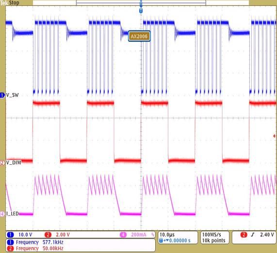
AX2020
BLOCK DIAGRAM
VIN V25
CS SW
- COMPARATOR
CSN +
130mV
GATE
DRIVER Driver
2.5V
-
70µ +
UVLO
COMPARATOR
GND
DIM
DIM
BUFFER
PIN ASSIGNMENT
The package of AX2020 is SOT89-5L; the pin assignment is given by:
Name Description
(Top View)
VIN CSN Switch Output. SW is the output of
SW
the internal driver switch.
5 GND 4
Signal and power ground. Connect
GND
directly to ground plane.
AX2020 Logic level dimming input. Drive
DIM low to turn off the current
DIM
regulator. Drive DIM high to enable
1 2 3 the current regulator.
CSN Current sense input
SW GND DIM
SOT89-5L Input Supply Pin. Must be locally
VIN
bypassed.
ORDER/MARKING INFORMATION
Order Information Top Marking
20 2 0 Part number
Y WX ID code: internal
WW: 01~26 (A~Z)
AX2020 XX X 27~52 (a~z)
Year: 8=2018
Package Type Packing 9=2019
F5: SOT89-5L Blank : Tube B=2020
A : Taping C=2021
D=2022
:
Z=2044
2/12
Axelite Confidential Materials, do not copy or distribute without written consent.
Rev.1.4 Sep.27, 2019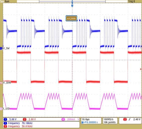
AX2020
ABSOLUTE MAXIMUM RATINGS (at TA=25°C)
Characteristics Symbol Rating Unit
Supply Voltage VIN -0.3 to 40 V
Driver output Voltage SW -0.3 to 40 V
Current sense input (Respect to VIN) CSN +0.3 to (-6.0) V
Logic level dimming input DIM -0.3 to +6 V
Switch output current ISW 1.2 A
Power Dissipation PDMAX 1.5 W
Operation Junction Temperature Range TJ -40 to 125 °C
Storage Temperature TSTG -55 to 150 °C
Thermal Resistance from Junction to case θJC 15 °C/W
Thermal Resistance from Junction to ambient θJA 50 °C/W
Note: θJA is measured with the PCB copper are (need connect to tap) of approximately 1 in2 (Multi-layer).
ELECTRICAL CHARACTERISTICS
The following specifications apply for VIN = 12V, TA=25°C, unless specified otherwise.
Characteristics Symbol Conditions Min Typ Max Units
Input voltage VIN 8 - 32 V
Under voltage lock out VUVLO VIN rising - 7 - V
UVLO Hysterisis VUVLO_hys VIN falling - 1000 - mV
Max. Switching Frequency FSW - - 1 MHZ
Current Sense
Mean current sense threshold voltage VCSN VIN–VCSN 115 130 145 mV
Sense threshold hysteresis VCSN_hys - ±15 - %
CSN Pin Input Current ICSN VIN–VCSN = 50mV - 0.5 - μA
DIM Input
DIM input voltage High VDIM_H 2.0 - - V
DIM input voltage Low VDIM_L - - 0.3 V
Max. DIM Frequency fDIM fOSC = 500kHz - - 50 kHZ
Duty cycle range of low frequency
fDIM = 100Hz 0.02% - 1
dimming DPWM_LF
Brightness control range - 5000:1 -
3/12
Axelite Confidential Materials, do not copy or distribute without written consent.
Rev.1.4 Sep.27, 2019AX2020
ELECTRICAL CHARACTERISTICS (CONTINUOUS)
The following specifications apply for VIN = 12V, TA=25°C, unless specified otherwise.
Duty cycle range of high frequency
fDIM = 20kHz 4% - 1
dimming DPWM_HF
Brightness control range - 25:1 -
DIM pull up resistor to Internal
RDIM - 300 - KΩ
supply voltage
DIM input leakage low IDIM_L VDIM = 0 - 70 - μA
Output Switch
Saturation Voltage VSAT IOUT = 0.3A - 0.8 1.0 V
Saturation Voltage VSAT IOUT = 0.8A - 1.0 1.2 V
Continuous SW Current ISWmean - - 1.0 A
SW Leakage Current ILEAK - 0.5 5 μA
Thermal Shutdown
Thermal Shutdown Threshold TSD - 150 - °C
Thermal Shutdown hysteresis TSD-hys - 35 - °C
APPLICATION CIRCUIT
RS L1
VIN 1W LED
0.4 47uH
CIN 4.7uF~100uF D
VIN CSN SW
DIM AX2020
GND
VCSN 0.130
ILED = = = 0.325A
RS 0.4
4/12
Axelite Confidential Materials, do not copy or distribute without written consent.
Rev.1.4 Sep.27, 2019AX2020
APPLICATION INFORMATION
OPERATION DESCRIPTION
The device, in conjunction with the coil (L1) and current sense resistor (RS), forms a
self oscillating continuous-mode buck converter.
When input voltage VIN is first applied, the initial current in L1 and RS is zero and there
is no output from the current sense circuit. Under this condition, the output of CS comparator
is high. This turns on an internal switch and switches the SW pin low, causing current to flow
from VIN to ground, via RS, L1 and the LED(s). The current rises at a rate determined by V IN
and L1 to produce a voltage ramp (VCSN) across RS. When (VIN-VCSN) > 150mV, the output of
CS comparator switches low and the switch turns off. The current flowing on the RS
decreases at another rate. When (VIN-VCSN) < 110mV, the switch turns on again and the
mean current on the LED is determined by ( 110 + 150 mV) / RS= 130mV / RS.
2
The high-side current-sensing scheme and on-board current-setting circuitry minimize
the number of external components while delivering LED current with ±5% accuracy, using a
1% sense resistor.
The AX2020 allow dimming with a PWM signal at the DIM input. A logic level below
0.3V at DIM forces AX2020 to turn off the LED and the logic level at DIM must be at least
2.0V to turn on the full LED current. The frequency of PWM dimming ranges from 100Hz to
more than 20 kHz.
The DIM pin is pulled high current approximately 70μA. It can be floated at normal
working. When a voltage applied to DIM falls below the threshold (0.3V nom.), the output
switch is turned off. The internal regulator and voltage reference remain powered during
shutdown to provide the reference for the shutdown circuit.
Additionally, to ensure the reliability, the AX2020 is built with a thermal shutdown (TSD)
protection and a thermal pad. The TSD protests the IC from over temperature (150°C). Also
the thermal pad enhances power dissipation. As a result, the AX2020 can handle a large
amount of current safely.
Setting nominal average output current with external resistor RS
The nominal average output current in the LED(s) is determined by the value of the
external current sense resistor (RS) connected between VIN and CSN and is given by:
IOUT = 0.130/RS (RS ≧ 0.16Ω)
This equation is valid when DIM pin is float. Actually, RS sets the maximum average
current which can be adjusted to a less one by dimming.
5/12
Axelite Confidential Materials, do not copy or distribute without written consent.
Rev.1.4 Sep.27, 2019AX2020
Output current adjustment by PWM control
A Pulse Width Modulated (PWM) signal with duty cycle PWM can be applied to the
DIM pin, as shown below, to adjust the output current to a value below the nominal average
value set by resistor RS:
0.13 × D
IOUT =
RS
(0≦D≦100%, 0.3V<Vpulse<2.5V)
RS L
VIN
0.4 47uH
CIN 4.7uF~100uF D
VIN CSN SW
DIM AX2020
PWM GND
PWM dimming provides reduced brightness by modulating the LED’s forward current
between 0% and 100%. The LED brightness is controlled by adjusting the relative ratios of
the on time to the off time. A 25% brightness level is achieved by turning the LED on at full
current for 25% of one cycle. To ensure this switching process between on and off state is
invisible by human eyes, the switching frequency must be greater than 100 Hz. Above 100
Hz, the human eyes average the on and off times, seeing only an effective brightness that is
proportional to the LED’s on-time duty cycle. The advantage of PWM dimming is that the
forward current is always constant; therefore the LED color does not vary with brightness as
it does with analog dimming. Pulsing the current provides precise brightness control while
preserving the color purity. The dimming frequency of AX2020 can be as high as 20 kHz.
Shutdown mode
Taking the DIM pin to a voltage below 0.3V will turn off the output and the supply
current will fall to a low standby level of 70μA nominal.
6/12
Axelite Confidential Materials, do not copy or distribute without written consent.
Rev.1.4 Sep.27, 2019AX2020
Capacitor selection
A low ESR capacitor should be used for input decoupling, as the ESR of this capacitor
appears in series with the supply source impedance and lowers overall efficiency. This
capacitor has to supply the relatively high peak current to the coil and smooth the current
ripple on the input supply. A minimum value of 4.7uF is acceptable if the input source is
close to the device, but higher values will improve performance at lower input voltages,
especially when the source impedance is high. The input capacitor should be placed as
close as possible to the IC.
For maximum stability over temperature and voltage, capacitors with X7R, X5R, or
better dielectric are recommended. Capacitors with Y5V dielectric are not suitable for
decoupling in this application and should not be used.
Inductor selection
Recommended inductor values for the AX2020 are in the range 47uH to 120uH.
Higher values of inductance are recommended at lower output current in order to minimize
errors due to switching delays, which result in increased ripple and lower efficiency. Higher
values of inductance also result in a smaller change in output current over the supply voltage
range. The inductor should be mounted as close to the device as possible with low
resistance connections to the SW and VIN pins.
Diode selection
For maximum efficiency and performance, the rectifier (D1) should be a fast low
capacitance Schottky diode with low reverse leakage at the maximum operating voltage and
temperature.
They also provide better efficiency than silicon diodes, due to a combination of lower
forward voltage and reduced recovery time.
It is important to select parts with a peak current rating above the peak coil current and
a continuous current rating higher than the maximum output load current. It is very important
to consider the reverse leakage of the diode when operating above 85°C. Excess leakage
will increase the power dissipation in the device and if close to the load may create a thermal
runaway condition.
The higher forward voltage and overshoot due to reverse recovery time in silicon
diodes will increase the peak voltage on the SW output. If a silicon diode is used, care
should be taken to ensure that the total voltage appearing on the SW pin including supply
ripple, does not exceed the specified maximum value.
7/12
Axelite Confidential Materials, do not copy or distribute without written consent.
Rev.1.4 Sep.27, 2019AX2020
Reducing output ripple
Peak to peak ripple current in the LED(s) can be reduced, if required, by shunting a
capacitor CLED across the LED(s) as shown below:
L
VIN
0.4 47uH
CLED
D 1uF
CIN 4.7uF~100uF
VIN CSN SW
DIM AX2020
GND
A value of 1uF will reduce the supply ripple current by a factor three (approx.).
Proportionally lower ripple can be achieved with higher capacitor values. Note that the
capacitor will not affect operating frequency or efficiency, but it will increase start-up delay
and reduce the frequency of dimming, by reducing the rate of rise of LED voltage.
By adding this capacitor the current waveform through the LED(s) changes from a
triangular ramp to a more sinusoidal version without altering the mean current value.
Operation at low supply voltage
The internal regulator disables the drive to the switch until the supply has risen above
the startup threshold (VUVLO). Above this threshold, the device will start to for this reason, the
temperature coefficients of the operating. However, with the supply voltage below the
specified minimum value, the switch duty cycle will be high and the device power dissipation
will be at a maximum. Care should be taken to avoid operating the device under such
conditions in the application, in order to minimize the risk of exceeding the maximum allowed
die temperature. (See next section on thermal considerations). The drive to the switch is
turned off when the supply voltage falls below the under-voltage threshold (VUVLO-1V).
This prevents the switch working with excessive 'on' resistance under conditions where
the duty cycle is high.
Thermal shutdown protection
To ensure the reliability, the AX2020 is built with a thermal shutdown (TSD) protection
function. The TSD protests the IC from over temperature (150°C). When the chip
temperature decreases (115°C), the IC recovers again.
8/12
Axelite Confidential Materials, do not copy or distribute without written consent.
Rev.1.4 Sep.27, 2019AX2020
TYPICAL CHARACTERISTICS
VIN VS. ICCQ VIN VS. DIMMING T HRESHOLD VOLTAGE
2.6 1
2.55
2.5 0.98
2.45 ↑Turn On
VDIM-THRESHOLD
2.4 0.96
ICCQ
2.35
(mA)
2.3 0.94
2.25 ↓Turn Off
2.2
0.92
2.15
2.1
0.9
8 12 16 20 24 28 32 8 12 16 20 24 28 32
VIN (V) VIN (V)
VIN VS. FREQUENCY (L=47μH) VIN VS. FREQUENCY (L=120μH)
700 500
600 400
FREQUENCY (KHz)
FREQUENCY (KHz)
500 300
400 200
300 100
200 0
8 12 16 20 24 28 32 8 12 16 20 24 28 32
VIN (V) VIN (V)
TEMPERATURE VS. ICCQ VIN=12V
5
4
3
ICCQ (mA)
2
1
0
-40℃ -20℃ 0℃ 25℃ 50℃ 85℃ 105℃ 125℃
Temperature
9/12
Axelite Confidential Materials, do not copy or distribute without written consent.
Rev.1.4 Sep.27, 2019AX2020
TYPICAL CHARACTERISTICS (CONTINUOUS)
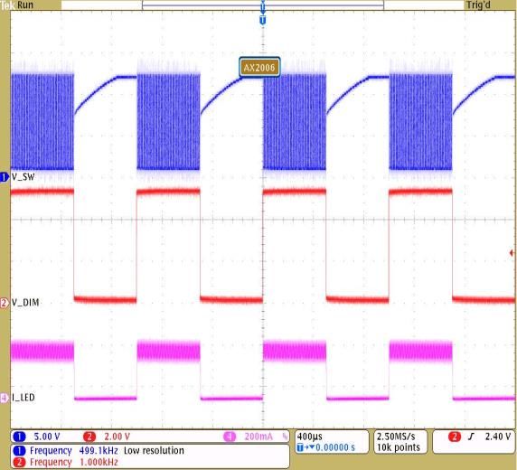
50KHz Dimming VIN=32V 50KHz Dimming VIN=12V
1KHz Dimming
10/12
Axelite Confidential Materials, do not copy or distribute without written consent.
Rev.1.4 Sep.27, 2019AX2020
PACKAGE OUTLINES
A
C
1.8
I
M
Q F
E B
4.6
P
N
0.6
1.2
F
1.1
0.6
I I
0.55
H 1.5
G Lead Pattern Recommendation (Unit: mm)
L
J
K
Dimensions in Millimeters Dimensions in Inches
Symbol
Min. Nom. Max. Min. Nom. Max.
A 4.4 4.5 4.6 0.173 0.177 0.181
B 4.05 4.15 4.25 0.159 0.163 0.167
C 1.4 1.6 1.7 0.055 0.062 0.067
E 2.4 2.5 2.6 0.094 0.098 0.102
F 0.8 - - 0.031 - -
G 3.00 REF. 0.118 REF.
H 1.50 REF. 0.059 REF.
I 0.36 0.46 0.53 0.014 0.018 0.02
J 1.4 1.5 1.6 0.055 0.059 0.063
K 0.35 0.39 0.43 0.014 0.015 0.017
L 8 TYP.
o 8 TYP.
o
M 0.38 0.47 0.6 0.015 0.019 0.024
N 0.2 0.18 0.4 0.008 0.007 0.026
P 0.48 0.57 0.67 0.019 0.022 0.027
Q - - 0.4 - - 0.016
JEDEC outline: NA
11/12
Axelite Confidential Materials, do not copy or distribute without written consent.
Rev.1.4 Sep.27, 2019AX2020
Carrier tape dimension
SOT89-5L
12/12
Axelite Confidential Materials, do not copy or distribute without written consent.
Rev.1.4 Sep.27, 2019You can also read