Electrically Parallel Three-Element 980 nm VCSEL Arrays with Ternary and Binary Bottom DBR Mirror Layers - MDPI

Page created by Brandon Norris
 
CONTINUE READING
Electrically Parallel Three-Element 980 nm VCSEL Arrays with Ternary and Binary Bottom DBR Mirror Layers - MDPI
materials
Article
Electrically Parallel Three-Element 980 nm VCSEL Arrays with
Ternary and Binary Bottom DBR Mirror Layers
Nasibeh Haghighi and James A. Lott *

                                          Faculty II Mathematics and Natural Sciences, Institute of Solid-State Physics, Center of Nanophotonics,
                                          Technische Universität Berlin, 10623 Berlin, Germany; nasibeh.haghighi@tu-berlin.de
                                          * Correspondence: james.lott@tu-berlin.de

                                          Abstract: To meet the performance goals of fifth generation (5G) and future sixth generation (6G)
                                          optical wireless communication (OWC) and sensing systems, we seek to develop low-cost, reliable,
                                          compact lasers capable of sourcing 5–20 Gb/s (ideally up to 100 Gb/s by the 2030s) infrared beams
                                          across free-space line-of-sight distances of meters to kilometers. Toward this end, we develop small
                                          arrays of electrically parallel vertical cavity surface emitting lasers (VCSELs) for possible future use
                                          in short-distance (tens of meters) free-space optical communication and sensing applications in, for
                                          example, homes, data centers, manufacturing spaces, and backhaul (pole-to-pole or pole-to-building)
                                          optical links. As a starting point, we design, grow by metal–organic vapor phase epitaxy, fabricate,
                                          test, and analyze 980 nm top-emitting triple VCSEL arrays. Via on-wafer high-frequency probe
                                          testing, our arrays exhibit record bandwidths of 20–25 GHz, optical output powers of 20–50 mW,
                                          and error-free data transmission at up to 40 Gb/s—all extremely well suited for the intended 5G
                                          short-reach OWC and sensing applications. We employ novel p-metal and top mesa inter-VCSEL
                                          connectors to form electrically parallel but optically uncoupled (to reduce speckle) arrays with
                                          performance exceeding that of single VCSELs with equal total emitting areas.

         
                                   Keywords: VCSEL; vertical cavity surface emitting laser; optical wireless communication; optical
                                          interconnects; free-space optical communication; fifth generation (5G); sixth generation (6G)
Citation: Haghighi, N.; Lott, J.A.
Electrically Parallel Three-Element
980 nm VCSEL Arrays with Ternary
and Binary Bottom DBR Mirror
Layers. Materials 2021, 14, 397.
                                          1. Introduction
https://doi.org/10.3390/ma14020397              We design, fabricate, and test three-element (triple) electrically parallel 980 nm vertical
                                          cavity surface emitting laser (VCSEL) arrays. We employ a new VCSEL epitaxial design
Received: 8 December 2020                 that includes a mix of binary (AlAs and GaAs) and ternary (AlGaAs) bottom distributed
Accepted: 11 January 2021                 Bragg reflector (DBR) layers. Binary DBR layers reduce thermal resistance and increase
Published: 14 January 2021                rollover current [1–3]. We simultaneously achieve high bandwidth (20–25 GHz), high
                                          power conversion efficiency (~30%), and relatively high (for only three VCSELs) optical
Publisher’s Note: MDPI stays neutral      output power (20–50 mW) as part of our quest to develop a key enabling component for
with regard to jurisdictional claims in   short-distance (meters to tens of meters) fifth generation (5G) and sixth generation (6G)
published maps and institutional affil-   optical wireless (free-space) communication networks and sensing systems.
iations.                                        We present our motivation and a brief history of VCSEL arrays designed specifically
                                          for free-space optical communication. We disclose a new epitaxial VCSEL layer design with
                                          a bottom distributed Bragg reflector that includes AlAs (binary) layers. We next describe
                                          our triple VCSEL array geometry and our on-wafer device testing methods. Finally, we
Copyright: © 2021 by the authors.         present new on-wafer measured results, briefly analyze the results, and, for the first time,
Licensee MDPI, Basel, Switzerland.        compare our measured emission spectra to simulated cold cavity two-dimensional (2D)
This article is an open access article    near-field surface mode wavelengths.
distributed under the terms and
conditions of the Creative Commons        1.1. Motivation
Attribution (CC BY) license (https://
                                               State-of-the-art fourth generation (4G) mobile networks employ the long-term evolu-
creativecommons.org/licenses/by/
                                          tion (4G-LTE) standard and operate at up to 100 megabits per second (Mb/s), although
4.0/).

Materials 2021, 14, 397. https://doi.org/10.3390/ma14020397                                                  https://www.mdpi.com/journal/materials
Electrically Parallel Three-Element 980 nm VCSEL Arrays with Ternary and Binary Bottom DBR Mirror Layers - MDPI
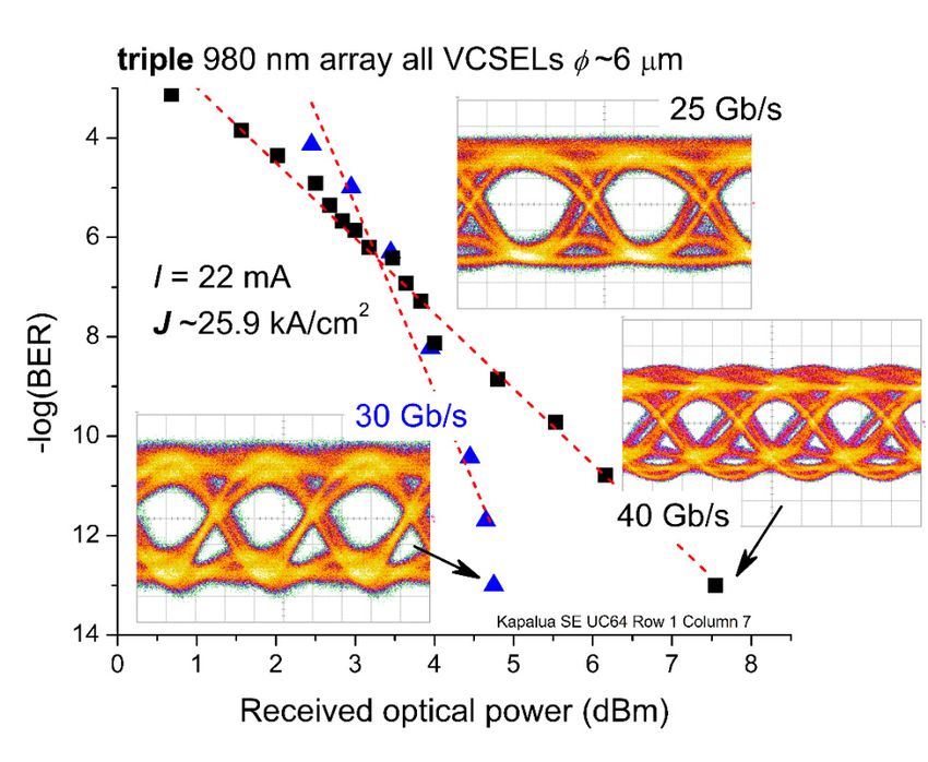
Materials 2021, 14, 397                                                                                               2 of 17

                          the average downloading data rate is only 33.88 Mb/s [4]. These networks enable high-
                          definition (HD) multimedia communication such as streaming high-definition movies and
                          online gaming. The new 5G mobile wireless infrastructure (now in the early deployment
                          stage) promises to add a plethora of ubiquitous and novel communication and sensing
                          devices and systems to existing networks, enabling massive scales of data generation, data
                          transfer, and data storage with anticipated data rates of 5 Gb/s to possibly 20 Gb/s via
                          millimeter wave transmission.
                                The 5G era promises extreme mobile coverage, mixed virtual reality, and low-latency
                          (aiming at
Electrically Parallel Three-Element 980 nm VCSEL Arrays with Ternary and Binary Bottom DBR Mirror Layers - MDPI
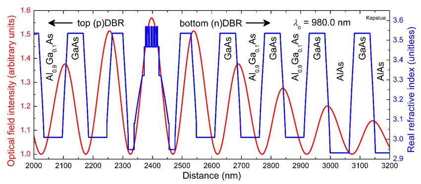
In [18], we reported the static and dynamic characteristics of a three-element electri-
                               cally parallel, optically uncoupled 980 nm VCSEL array with ϕ~7.5 μm. We achieved a
                               maximum f3dB of ~24 GHz, WPEmax of ~36%, and Lmax of ~27 mW. In this new work, we
                               characterize a binary DBR version of the same triple-array geometry but over a much
    Materials 2021, 14, 397    larger range of oxide aperture diameters, from ϕ~6 μm to 17 μm. In a new key3 of  17 of f3dB
                                                                                                               plot
                               versus L (with ϕ~6, 9, and 14 μm), we illustrate the possible bandwidth–optical output
                               power combinations of our three-element electrically parallel arrays.
                                    a maximum f 3dB of ~24 GHz, WPEmax of ~36%, and Lmax of ~27 mW. In this new work,
                                    we  characterize
                               2. Materials          a binary DBR version of the same triple-array geometry but over a much
                                              and Methods
                                    larger range of oxide aperture diameters, from φ~6 µm to 17 µm. In a new key plot of f 3dB
                                    We disclose
                                    versus          in three
                                            L (with φ~6,  9, andsubsections  our VCSEL
                                                                 14 µm), we illustrate      epitaxial
                                                                                       the possible     material layeroutput
                                                                                                    bandwidth–optical  design, our
                               three-element    VCSEL array
                                    power combinations    of our physical  geometry
                                                                 three-element          andparallel
                                                                               electrically fabrication
                                                                                                    arrays.methods, and finally our
                               on-wafer VCSEL testing methods.
                                     2. Materials and Methods
                                        WeEpitaxial
                               2.1. VCSEL disclose inDesign
                                                      three subsections our VCSEL epitaxial material layer design, our three-
                                     element VCSEL array physical geometry and fabrication methods, and finally our on-wafer
                                     We grew
                                     VCSEL       980methods.
                                            testing  nm VCSEL material layers on highly n-doped (001) surface-oriented
                               GaAs substrates via metal–organic vapor phase epitaxy (MOVPE)—in batches of 12, 3
                               inch 2.1.   VCSEL
                                      wafers     perEpitaxial
                                                       growth Design
                                                                 run. For the particular wafer set reported herein—our Kapalua
                                            We grew design—we
                               VCSEL epitaxial          980 nm VCSELstartedmaterial   layers
                                                                                    with   200onnmhighly   n-doped (001)
                                                                                                      of undoped             surface-oriented
                                                                                                                        (u)GaAs;       then, in succes-
                                     GaAs substrates via metal–organic vapor phase epitaxy (MOVPE)—in batches of 12, 3 inch
                               sion, we grew 5 nm of graded (u)AlxGa1−xAs (with x varying from 0.0 to 1.0), 157 nm of
                                     wafers per growth run. For the particular wafer set reported herein—our Kapalua VCSEL
                               (u)AlAs,     10 nm of graded (u)AlxGa1−xAs (x = 1.0 to 0.0), and 1580 nm of GaAs highly n-
                                     epitaxial design—we started with 200 nm of undoped (u)GaAs; then, in succession, we
                               doped     with
                                     grew 5 nm   silicon.  This(u)Al
                                                    of graded    thick    (n+)GaAs layer served as an n-metal (cathode) ohmic con-
                                                                      x Ga1−x As (with x varying from 0.0 to 1.0), 157 nm of (u)AlAs,
                               tact layer.
                                     10 nm The      VCSEL
                                               of graded      epitaxial
                                                           (u)Al x Ga1−x As structure    followed,
                                                                               (x = 1.0 to  0.0), and including
                                                                                                       1580 nm ofin      sequence,
                                                                                                                      GaAs                a 34-period n-
                                                                                                                               highly n-doped
                               doped with   silicon. Thisdistributed
                                         AlAs/GaAs          thick (n+)GaAs Bragg layer  served (DBR)
                                                                                    reflector    as an n-metal
                                                                                                          with 18(cathode)
                                                                                                                    nm thick     ohmic
                                                                                                                                     gradedcontact
                                                                                                                                                interfaces
                                     layer.  The   VCSEL   epitaxial  structure   followed,  including
                               (from an AlAs mole fraction x = 1.0 to 0.0 and vice versa), a three-period in sequence,   a 34-period     n-doped
                                     AlAs/GaAs distributed Bragg reflector (DBR) with 18 nm thick graded interfaces (from
                               (n)Al0.9Ga0.1As/GaAs DBR with 18 nm thick graded interfaces (from x = 0.9 to 0.0 and vice
                                     an AlAs mole fraction x = 1.0 to 0.0 and vice versa), a three-period (n)Al0.9 Ga0.1 As/GaAs
                               versa),
                                     DBR  a with
                                            λ/2 optically
                                                  18 nm thick thick
                                                                gradedcavity,    and(from
                                                                          interfaces   a 15.5-period
                                                                                             x = 0.9 to 0.0p-doped
                                                                                                             and vice with
                                                                                                                       versa),carbon        top coupling
                                                                                                                                  a λ/2 optically
                                      0.9Gacavity,
                               (p)Althick    0.1As /GaAs     DBR (with
                                                      and a 15.5-period       the same
                                                                           p-doped    with18   nm thick
                                                                                            carbon           graded(p)Al
                                                                                                     top coupling      interfaces).       We employed
                                                                                                                            0.9 Ga0.1 As /GaAs
                               five In
                                     DBRyGa(with
                                             1−yAs the
                                                     (y ~0.23)
                                                         same 18quantum
                                                                    nm thickwells      (QWs)
                                                                                  graded         surrounded
                                                                                          interfaces).            by GaAs
                                                                                                           We employed          1−xPIn
                                                                                                                             five    xy(xGa~0.14)
                                                                                                                                             1−y As barrier
                                     (y  ~0.23)  quantum    wells  (QWs)    surrounded
                               layers and two, 20 nm thick (as grown) Al0.98Ga0.02As      by  GaAs      P   (x
                                                                                                    1−xlayers,
                                                                                                          x    ~0.14) barrier    layers
                                                                                                                 selectively thermally   and   two,
                                                                                                                                                 oxidized
                                     20  nm   thick  (as grown)  Al      Ga      As layers, selectively  thermally   oxidized
                               during device fabrication, centered on optical field intensity nodes, as shown in Figure 1.
                                                                    0.98    0.02                                                   during   device
                                     fabrication, centered on optical field intensity nodes, as shown in Figure 1.

Figure 1. Simulated
        Figure           one-dimensional
                1. Simulated                    optical
                              one-dimensional optical    field
                                                      field     intensity
                                                            intensity       on resonance
                                                                      on resonance (red curve)(red  curve)
                                                                                               and real      andindex
                                                                                                        refractive real refractive
                                                                                                                         (blue curve) index
(blue curve) along the epitaxial growth direction in and around the quantum well (QW) activenmregion
        along the  epitaxial growth direction in and around   the quantum   well (QW) active region for the Kapalua  980     verticalfor the
        cavity surface emitting laser (VCSEL) design.
Kapalua 980 nm vertical cavity surface emitting laser (VCSEL) design.
Electrically Parallel Three-Element 980 nm VCSEL Arrays with Ternary and Binary Bottom DBR Mirror Layers - MDPI
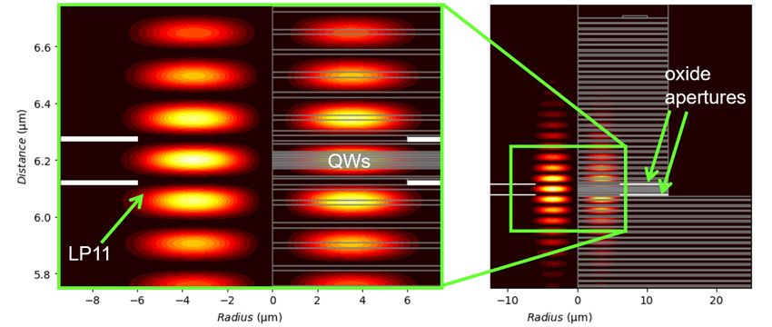
Materials 2021, 14, x FOR PEER REVIEW                                                                                                                  4 of 18

        Materials 2021, 14, 397
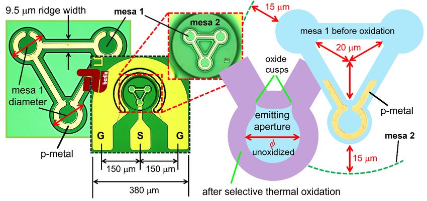
                                   2.2. VCSEL Array Geometry and Fabrication                                                                 4 of 17
                                          We fabricated VCSELs on quarter wafer pieces in our university cleanroom and ther-
                                   mal oxidation laboratory; see Figure 2 for images and illustrations of our three-element
                                   (triple)  VCSELArray
                                        2.2. VCSEL       array     deviceand
                                                               Geometry       geometry.
                                                                                  FabricationWe deposited ZnAu/Au p-metal (with cut open
                                   rings plus Weinter-ring
                                                   fabricated metal
                                                                  VCSELslines)       via thermal
                                                                              on quarter               evaporation,
                                                                                             wafer pieces                 and then
                                                                                                              in our university        etched circular
                                                                                                                                    cleanroom      and      top
                                   mesas    just  through      the     optical   cavity    with   Cl   +  BCl    in  a SENTECH
                                        thermal oxidation laboratory; see Figure 2 for images and illustrations of our three-element
                                                                                                     2         3                      Instruments       GmbH
                                   SI 500   (Berlin,
                                        (triple) VCSEL  Germany)
                                                            array deviceinductively
                                                                              geometry.coupled       plasma
                                                                                           We deposited          (ICP) reactive
                                                                                                             ZnAu/Au       p-metalion    etching
                                                                                                                                     (with  cut open(RIE) sys-
                                        rings  plus   inter-ring    metal   lines)   via thermal   evaporation,      and
                                   tem using photoresist as an etching mask. We monitored the etch depth in situ (during  then  etched   circular  top
                                        mesas justetching)
                                   the ICP-RIE       through the  byoptical    cavity the
                                                                        measuring       withoptical
                                                                                             Cl2 + BCl   3 in a SENTECH
                                                                                                       power     reflectance Instruments
                                                                                                                                 of several GmbH
                                                                                                                                               wafer SI surface
                                        500 (Berlin, Germany) inductively coupled plasma (ICP) reactive ion etching (RIE) system
                                   points   at λo = 632.8 nm. After performing a selective thermal oxidation at 420 °C at 50 mbar
                                        using photoresist as an etching mask. We monitored the etch depth in situ (during the
                                   in a ICP-RIE
                                        chamberetching)
                                                     filled with        N2 + H2Othe
                                                               by measuring          vapor,   wepower
                                                                                         optical   etched     a secondofcircular
                                                                                                           reflectance       several mesa
                                                                                                                                      wafer down
                                                                                                                                              surfacejust into
                                   the 1580
                                        pointsnm    thick
                                                 at λ        (n+)GaAs
                                                       o = 632.8            and performing
                                                                    nm. After       then deposited       Ni/AuGe/Au
                                                                                                  a selective                n-metal (cathode)
                                                                                                                 thermal oxidation      at 420 ◦ C at in horse-
                                   shoe50shapes
                                            mbar in around
                                                        a chamberthe filled
                                                                        bottom withmesas.
                                                                                       N2 + HNext,     we spun-on
                                                                                               2 O vapor,    we etched   and  pre-baked
                                                                                                                           a second          photosensitive
                                                                                                                                      circular   mesa
                                        down just into the
                                   benzocyclobutene          (BCB)1580to nm   thick
                                                                           help       (n+)GaAsthe
                                                                                   planarize      and   then deposited
                                                                                                      arrays   (to createNi/AuGe/Au          n-metalfor sub-
                                                                                                                             a quasi-flat surface
                                        (cathode) in horseshoe shapes around the bottom mesas. Next, we spun-on and pre-baked
                                   sequent pad metal deposition), and then exposed the BCB to ultraviolet (UV) radiation
                                        photosensitive benzocyclobutene (BCB) to help planarize the arrays (to create a quasi-flat
                                   and surface
                                          developed       (removed) BCB above the p-metal and n-metal. Lastly, we deposited
                                                  for subsequent pad metal deposition), and then exposed the BCB to ultraviolet
                                   Cr/Pt/Au     contact and
                                        (UV) radiation      metal      via standard
                                                                  developed      (removed)UVBCB
                                                                                              contact
                                                                                                    abovephotolithography
                                                                                                            the p-metal and n-metal.in a lift-off   process in
                                                                                                                                           Lastly, we
                                   the shape
                                        depositedof co-planar
                                                     Cr/Pt/Au contactground–signal–ground
                                                                              metal via standard UV    (GSG)     pads
                                                                                                           contact       to facilitate on-wafer
                                                                                                                     photolithography     in a lift-offprobing
                                   The process    in the shape
                                         linear spacing            of co-planar
                                                              of the     GSG pads   ground–signal–ground
                                                                                        (the center of the(GSG)   S padpads   to facilitate
                                                                                                                          to the  centerson-wafer
                                                                                                                                             of each G pad)
                                   was 150 μm. Our co-planar GSG pad configuration had a fixed width of 480ofμm
                                        probing.   The   linear   spacing   of  the  GSG   pads  (the  center  of  the S pad  to the centers      each(as indi-
                                        G pad) was 150 µm. Our co-planar GSG pad configuration had a fixed width of 480 µm (as
                                   cated in Figure 2) and heights that varied from roughly 350 (Row 0) to 370 μm (Row 9)
                                        indicated in Figure 2) and heights that varied from roughly 350 (Row 0) to 370 µm (Row 9).
                                   To facilitate    on-wafer
                                        To facilitate  on-wafer testing,
                                                                    testing, weweplaced
                                                                                     placedourour   triple
                                                                                               triple  arraysarrays
                                                                                                               withinwithin
                                                                                                                        the GSGthepadGSG     pad configura-
                                                                                                                                       configuration
                                   tion shown
                                         showninin      Figure
                                                    Figure        2, i.e.,
                                                              2, i.e.,     the same
                                                                       the same    contactcontact   pad geometry
                                                                                            pad geometry      we used for wesingle
                                                                                                                              used VCSELs.
                                                                                                                                     for single VCSELs.

            Figure
     Figure 2.      2. Illustration
               Illustration   of theoftriple
                                        the triple VCSEL
                                               VCSEL      array
                                                        array   geometry via
                                                               geometry    via aa collage
                                                                                   collageofof
                                                                                             microscope images
                                                                                               microscope      and schematics.
                                                                                                           images              We show
                                                                                                                    and schematics.  We show
            unoxidized    areas in light blue and  oxidized areas
     unoxidized areas in light blue and oxidized areas in purple. in purple.

                                              We constructed electrically parallel, optically uncoupled triple (three-element) 980 nm
                                         We constructed
                                       VCSEL                  electrically
                                                arrays with variable  oxide parallel,    opticallyand
                                                                             aperture diameters     uncoupled       triple (three-element)
                                                                                                        variable inter-VCSEL     pitch (sep-    980
                                   nm VCSEL       arrays with
                                        aration distance)       variable
                                                          as follows       oxide
                                                                      [17,18]. Theaperture
                                                                                    top mesasdiameters       and variable
                                                                                                (mesa 1) consisted   of threeinter-VCSEL
                                                                                                                               circles with pitch
                                   (separation
                                        identical distance)
                                                  diameters, as  follows
                                                              each         [17,18].
                                                                    centered on one The
                                                                                      of thetop  mesas
                                                                                             three        (mesa
                                                                                                   imaginary      1) consisted
                                                                                                               vertices            of three circles
                                                                                                                         of an equilateral
                                        triangle. The mesa  1 diameters  ranged  from  22  µm  (Row  0) to 31 µm  (Row   9).
                                   with identical diameters, each centered on one of the three imaginary vertices of an equi-We  connected
                                        the triangle.
                                   lateral  three top mesa  circles 1
                                                      The mesa      with 9.5 µm wide
                                                                      diameters         (rectangular)
                                                                                   ranged     from 22ridge
                                                                                                         μm connectors.
                                                                                                              (Row 0) toEach 31 μmtop (Row
                                                                                                                                      mesa, 9). We
                                        thus, had a distinct open triangular pattern with solid circular corners. We centered 3.5 µm
                                   connected the three top mesa circles with 9.5 μm wide (rectangular) ridge connectors. Each
                                       wide p-metal contacts on our top mesas, but with ring patterns on the three corners. We
                                   top mesa, thus, had a distinct open triangular pattern with solid circular corners. We cen-
                                   tered 3.5 μm wide p-metal contacts on our top mesas, but with ring patterns on the three
                                   corners. We electrically isolated the ridge connectors via selective thermal oxidation; thus
                                   we oxidized a minimum length of 9.5/2 μm in from the exposed mesa 1 edges after the
Electrically Parallel Three-Element 980 nm VCSEL Arrays with Ternary and Binary Bottom DBR Mirror Layers - MDPI
Materials 2021, 14, 397                                                                                          5 of 17

                          electrically isolated the ridge connectors via selective thermal oxidation; thus, we oxidized
                          a minimum length of 9.5/2 µm in from the exposed mesa 1 edges after the first dry etch,
                          and simultaneously formed circular oxide apertures within the metal rings (possibly with
                          negligible cusps as shown in Figure 2). The inter-VCSEL spacing (VCSEL center to VCSEL
                          center) varied from about 54 µm (Row 0) to 62 µm (Row 9). The three VCSELs (in each
                          array) shared a circular bottom mesa (mesa 2) with diameters ranging from 114 µm (Row 0)
                          to 132 µm (Row 9). The radial distance from the centers of the bottom mesas to the nearest
                          inner edges of the top mesas was constant at 20 µm for all triple arrays (Rows 0 to 9).
                          Likewise (see the dimensions in Figure 2), the radial distance from the outer edges of
                          the top mesas to the edges of bottom mesas was constant at 15 µm for all triple arrays
                          (Rows 0 to 9).

                          2.3. VCSEL Charcaterization Methods
                                We measured the triple VCSEL array characteristics using the methods and test
                          equipment we described in [17–20]. Herein, we performed all measurements at ambient
                          room temperature (RT ~23 ◦ C) on three separate test stations in our university laboratory.
                          We placed our fabricated quarter wafer pieces (one at a time) on a first probe station
                          platen (a flat metal surface with several small vacuum holes), holding the wafer in place
                          via a vacuum but otherwise without heat sinking. By means of high-frequency GSG
                          probes, we directly contacted the VCSEL array under test. Via our proprietary LabVIEW
                          (computer) program, we swept the bias current (I) with a Keithley 2400-LV current source
                          and measured the static light output power (L) and voltage (V), thus producing LIV curves.
                          We measured L with a calibrated integrating sphere which included a photodiode (PD,
                          with a wavelength sensitivity range well below and above 980 nm). With another Keithley
                          2400-LV, we measured the current from the integrating sphere plus PD and converted
                          the current to an optical power. We placed a 90% blocking neutral density filter (with
                          antireflecting coatings at 980 nm) between our VCSEL under test and the entrance to the
                          integrating sphere to limit the input optical power. On a second probe station, we placed a
                          GSG probe onto the VCSEL array and applied a static (direct current, DC) as before via
                          a LabVIEW program (either a fixed bias current or a series of bias currents). We placed
                          a cleaved-end OM1 multiple-mode optical fiber (MMF) directly onto the three VCSELs
                          (butt-coupled). We connected the opposing end of the OM1 MMF patch cord (typically
                          0.5 or 1 m in length) to an Ando model AQ 6317C optical spectrum analyzer (Yokogawa
                          Electric Company Limited, Hiroshima, Japan) and recorded the emission spectra.
                                On the same second probe station, we performed small-signal frequency response (i.e.,
                          S21 scattering parameter) measurements under the control of another LabVIEW program
                          via standard daisy-chained general-purpose interface bus (GPIB) cables connected to the
                          test equipment. We connected port 2 of an Hewlett-Packard 8722C (Palo Alto, CA, USA)
                          Vector Network Analyzer (VNA) to our VCSEL via a high-frequency metal line and GSG
                          probe (which electrically excited the VCSEL array with a direct current (DC) bias (from
                          a Keithley 2400-LV current source) plus a sinusoidal −20 dBm (10 µW) source signal
                          created by the VNA. We butt-coupled the same OM1 MMF (used in our spectral emission
                          measurement) to the VCSEL array under test and connected the opposing end to a New
                          Focus (San Jose, CA, USA) model 1424 photodetector with a bandwidth of 25 GHz. The
                          New Focus photodetector was connected directly to the VNA’s port 1. We calibrated the
                          VNA test setup to mitigate errors prior to our S21 measurements. Note that we (actually)
                          measured the S12 parameters since we connected the VNA’s port 2 (electrically) to the
                          VCSEL via a high-frequency (HF) transmission line and we connected the photoreceiver
                          (electrically) to the VNA’s port 1. Since the VNA was a two-port two-path VNA, the port
                          connections were interchangeable. This was simply because port 2 was closer to our probe
                          station and VCSEL under test. The result was identical if we switched the port connections.
                          By convention, we report the frequency response as S21 parameters.
Electrically Parallel Three-Element 980 nm VCSEL Arrays with Ternary and Binary Bottom DBR Mirror Layers - MDPI
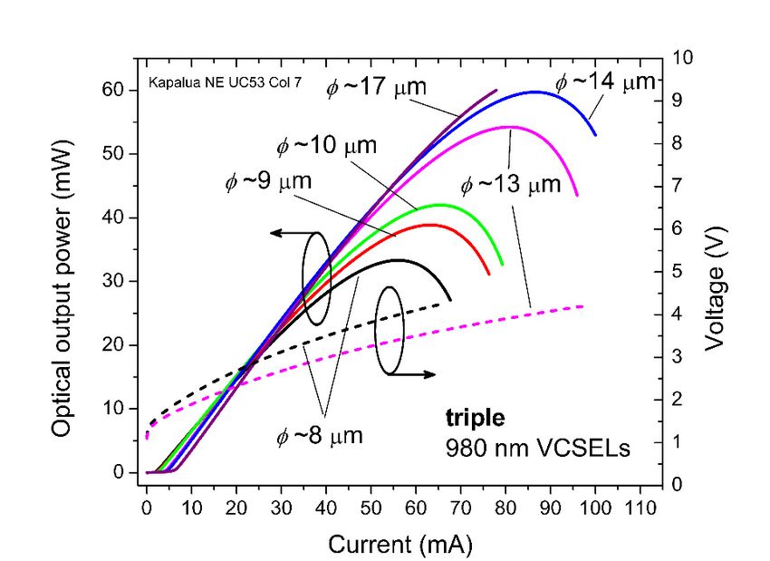
Materials 2021, 14, 397                                                                                           6 of 17

                                Lastly, for data transmission measurements using two-level pulse amplitude modula-
                          tion at 25 to 40 Gb/s (see [18] for a schematic of the test setup), we placed the fabricated
                          wafers onto a third test station and made electrical contact with a GSG probe on one array
                          at a time. Via an SHF 12100B (Berlin, Germany) bit pattern generator (which received
                          a clocking signal from an Agilent E8257D (Santa Clara, CA, USA) signal generator) and
                          a bias-tee, we excited the VCSEL array with a DC bias current plus (as a large signal
                          peak-to-peak voltage (typically ~610 mV) on top of the DC bias), a standard pseudorandom
                          bit (or binary) sequence (PRBS) of word length 27 − 1.
                                Via an OM1 MMF patch cord (~1 m in length), we coupled the array emission into
                          a highly sensitive u2t (Berlin, Germany) photoreceiver (a custom-built PD and amplifier
                          with a bandwidth of 30 GHz), and, in turn, we sent the resultant electrical signal into either
                          an Agilent DCA J86100C (Santa Rosa, CA, USA) digitizing oscilloscope (to measure eye
                          patterns) or into an SHF 11100B (Berlin, Germany) error analyzer (ER) to measure the bit
                          error ratio. We first optimized the eye pattern at 40 Gb/s by adjusting the bias current, the
                          magnitude of the peak-to-peak large signal PRBS signal, and, if necessary, the position of
                          the OM1 MMF. We then switched the OM1 MMF from the digitizing oscilloscope to the
                          error analyzer, and, while measuring the bit error ratio (BER) in real time, we tweaked the
                          voltage detection level (within the eye pattern) to optimize the BER. Then, we proceeded
                          with the actual BER test measurements. First, without optical attenuation, we ran the
                          PRBS for 30 s or longer and recorded the BER. We measured the optical power entering
                          the u2t photoreceiver with a JDSU OLP-55 (Milpitas, CA, USA) optical power meter. We
                          then repeatedly reconnected the fiber to the u2t photoreceiver, added ever higher optical
                          attenuation (to add errors) using a JDSU OLA-54 variable optical attenuator, and repeated
                          the BER measurement.

                          3. Results
                               We performed all measurements at room temperature (the ambient T was ~23 ◦ C) in
                          our university laser diode testing laboratory without heat sinking via on-wafer probing.
                          Herein, we present results from two fabricated quarter wafer pieces (from a 3 inch diameter
                          starting wafer), designated Kapalua NE (which we thermally selectively oxidized for
                          111 min) and Kapalua SE (which we thermally selectively oxidized for 135 min). Each
                          processed quarter wafer contained roughly eight unit cells (UCs). Each repeated unit cell
                          contained 184 VCSELs (single VCSELs, triple VCSEL arrays, septuple VCSEL arrays, and
                          more). We focus herein solely on selected columns of triple VCSELs (groups of 10 adjacent
                          triple arrays in Rows 0 to 9 in each unit cell). The triple VCSEL arrays on Kapalua NE
                          had oxide aperture diameters ranging from ~8 to 17 µm (Rows 0 to 9) with corresponding
                          top mesa diameters of 22 to 31 µm, whereas the triple VCSEL arrays on Kapalua SE had
                          oxide aperture diameters ranging from ~5 to 14 µm (Rows 0 to 9) with the same top mesa
                          (mesa 1) diameters.

                          3.1. Static Optical Output Power–Current–Voltage Characteristitcs
                               In Figure 3, we plot example static (direct current, DC) LIV curves for triple 980 nm
                          VCSEL arrays with variable oxide aperture diameters from (estimated) φ~8 to 17 µm. The
                          maximum L (at the LI rollover points) vary from about 30 mW (or ~10 mW per φ~8 µm
                          VCSEL) to more than 60 mW (or ~20 mW per φ~17 µm VCSEL). The triple VCSEL array
                          (on the NE quarter wafer) with φ~8 µm lies in Row 0 with a top mesa 1 diameter of 22 µm.
                          The triple VCSEL with φ~17 µm lies in Row 9 with a top mesa 1 diameter of 31 µm.
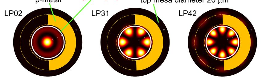
Electrically Parallel Three-Element 980 nm VCSEL Arrays with Ternary and Binary Bottom DBR Mirror Layers - MDPI
Materials 2021,
  Materials     14,14,
            2021,   x FOR  PEER
                       x FOR    REVIEW
                             PEER REVIEW                                                                                                                      7 of718of 18
     Materials 2021, 14, 397                                                                                                                                      7 of 17

                                    Figure 3. Measured static optical output power and voltage as functions of applied direct current
                                   Figure
                                    (DC)  3. Measured
                                         bias
                                       Figure current  forstatic
                                              3. Measured   980  optical
                                                                 nm
                                                              static      output
                                                                     triple
                                                                     opticalVCSELpower
                                                                                  arrays
                                                                             output     and
                                                                                    power   voltage
                                                                                         with
                                                                                          and oxide  as as
                                                                                                        functions
                                                                                                    aperture
                                                                                               voltage             ofof
                                                                                                                      applied
                                                                                                              diameters
                                                                                                           functions           direct
                                                                                                                         (ϕ) from
                                                                                                                        applied       current
                                                                                                                                   ~8 to
                                                                                                                                 direct  17
                                                                                                                                        current
                                    μm.(DC)
                                   (DC) biasbias
                                             current  for  980  nm   triple VCSEL  arrays with oxide  aperture  diameters   (ϕ) from  ~8
                                                 current for 980 nm triple VCSEL arrays with oxide aperture diameters (φ) from ~8 to 17   toµm.
                                                                                                                                             17
                                   μm.
                                              In In
                                                  Figure
                                                     Figure4, 4,
                                                              we weplot
                                                                      plotthe
                                                                            thecorresponding           differentialseries
                                                                                 corresponding differential             seriesresistance
                                                                                                                                  resistance(R(R  diff==∆V/
                                                                                                                                                diff       ΔV/∆IΔI ininΩ)
                                    Ω)and   In
                                          andthe Figure
                                                  thewall 4,  we
                                                       wallplug     plot   the
                                                              plugefficiency    corresponding
                                                                      efficiency(WPE(WPE= =100           differential
                                                                                                    ·L/(I·V) as
                                                                                                 100·L/(I·V)              series
                                                                                                                as aapercentage),    resistance
                                                                                                                       percentage),both   bothas   (R
                                                                                                                                                asfunctions =  Δ
                                                                                                                                                     functionsofof
                                                                                                                                                       diff       V/ Δthe
                                                                                                                                                                       I in
                                   Ω)
                                    theand
                                         applied the forward
                                            applied   wall   plug
                                                       forward    DC efficiency
                                                                    DC  bias
                                                                          biascurrent(WPE
                                                                                current    for=the
                                                                                         for      100·L/(I·V)
                                                                                                 the triple
                                                                                                       triplearraysas awith
                                                                                                               arrays    percentage),
                                                                                                                         with    ϕ~8µm
                                                                                                                               φ~8      μmand
                                                                                                                                            both
                                                                                                                                            and   ϕ~13
                                                                                                                                                φ~13     µm.μm.For
                                                                                                                                                    as functions   Fortheof
                                            ϕ~8µm
                                    theapplied
                                   the   φ~8       μmtriple
                                                       triple array,
                                                      forward       DCthe
                                                               array,    the maximum
                                                                          biasmaximum
                                                                                current for WPE           aboutarrays
                                                                                                  theistriple
                                                                                                         about     30%near
                                                                                                                  30%    near
                                                                                                                            withII==ϕ~8   μm
                                                                                                                                     1010mA,
                                                                                                                                          mA,while
                                                                                                                                                while
                                                                                                                                               and         Rdiff
                                                                                                                                                        Rdiff
                                                                                                                                                       ϕ~13     μm.drops
                                                                                                                                                               drops   For
                                    from
                                   the   from
                                         ϕ~8     μmroughly
                                               roughly    70 70
                                                      triple  Ω  Ω Iat= Ithe
                                                                 at
                                                               array,     = mA
                                                                         10  10  mA    to roughly
                                                                                   to roughly
                                                                              maximum         WPE   30 30
                                                                                                        Ω  Ω Iat= I5030%
                                                                                                           at
                                                                                                        is about     = mA.
                                                                                                                       50 mA.ForFor
                                                                                                                           near    Ithe the
                                                                                                                                         ϕ~13
                                                                                                                                      = 10 mA, μm
                                                                                                                                            φ~13    µm    triple
                                                                                                                                                     triple
                                                                                                                                                 while       Rarray,array,
                                                                                                                                                               diff drops
                                    the  the    maximum
                                            maximum        WPE WPE is  is about
                                                                      about    32% 32%nearnear
                                                                                            I
                                   from roughly 70 Ω at I = 10 mA to roughly 30 Ω at I = 50 mA. = I
                                                                                                  15=  15
                                                                                                       mA, mA,    while
                                                                                                              while    R   R
                                                                                                                        diff drops drops
                                                                                                                                       fromfrom   roughly
                                                                                                                             diffFor the ϕ~13 μm triple array,
                                                                                                                                             roughly       45  Ω45 atΩI at
                                    = 10
                                   the   I  =   10  mA   to
                                             mA to roughly
                                         maximum            roughly
                                                          WPE is  30about30  Ω  at
                                                                       Ω at I 32%  I  =
                                                                                = 45 mA.45  mA.
                                                                                       near Since   Since
                                                                                              I = 15the  mA,the
                                                                                                            threethree
                                                                                                               while     VCSELs
                                                                                                                     VCSELs            are electrically
                                                                                                                                  are electrically
                                                                                                                         Rdiff drops     from roughly       in parallel,
                                                                                                                                                       in parallel,
                                                                                                                                                               45 Ω at I
                                    R    Ris
                                       diff diff  is one-third
                                                one-third    the  the   differential
                                                                   differential         series
                                                                                    series        resistance
                                                                                             resistance      of  of one
                                                                                                                 one   of   of
                                                                                                                            thethe    three
                                                                                                                                  three     VCSELs
                                                                                                                                          VCSELs          (neglecting
                                                                                                                                                      (neglecting
                                   = 10 mA to roughly 30 Ω at I = 45 mA. Since the three VCSELs are electrically in parallel,
                                         any     resistance   differences      among  thethe    three   VCSELs       due
                                                                                                                       to to
                                                                                                                           thethe    array  geometry).
                                   Rany      resistance    differences      among          three     VCSELs      due
                                     diff is one-third the differential series resistance of one of the three VCSELs (neglecting
                                                                                                                                 array   geometry).
                                   any resistance differences among the three VCSELs due to the array geometry).

                                    Figure   4. Extracted
                                        Figure             differential
                                                 4. Extracted           series
                                                              differential     resistance
                                                                           series         andand
                                                                                  resistance  wall plug
                                                                                                 wall   efficiency
                                                                                                      plug         versus
                                                                                                           efficiency     DCDC
                                                                                                                      versus bias current
                                                                                                                                bias current for
                                    for the
                                         the 980
                                             980nmnmtriple
                                                      tripleVCSEL
                                                            VCSELarrays
                                                                     arraysininFigure
                                                                                Figure33with
                                                                                         withφ~8
                                                                                              ϕ~8and
                                                                                                  and13  μm.
                                                                                                       13µm.

                                   Figure 4. Extracted differential series resistance and wall plug efficiency versus DC bias current
                                             Next,
                                          Next,     in Figure
                                                in Figure      5, plot
                                                           5, we   we the
                                                                        plotunitless
                                                                              the unitless external
                                                                                     external         differential
                                                                                              differential quantum quantum     efficiency
                                                                                                                      efficiency  ηQE =
                                   for the 980 nm triple VCSEL arrays in Figure 3 with ϕ~8 and 13 μm.
                                         QE =Δ(qλ
                                    (qληo/hc)(         versus∆I)
                                               L/ΔoI)/hc)(∆L/    versusqI,iswhere
                                                              I, where             q is the
                                                                             the charge   oncharge on one electron,
                                                                                             one electron,          h is Planck’s
                                                                                                           h is Planck’s  constant,constant,
                                                                                                                                     λo is
                                       λo is the emission wavelength (980 nm), and c is the speed of light. We also plot, in Figure 5,
                                        Next, in Figure 5, we plot the unitless external differential quantum efficiency ηQE =
                                   (qλo/hc)(ΔL/ΔI) versus I, where q is the charge on one electron, h is Planck’s constant, λo is
Electrically Parallel Three-Element 980 nm VCSEL Arrays with Ternary and Binary Bottom DBR Mirror Layers - MDPI
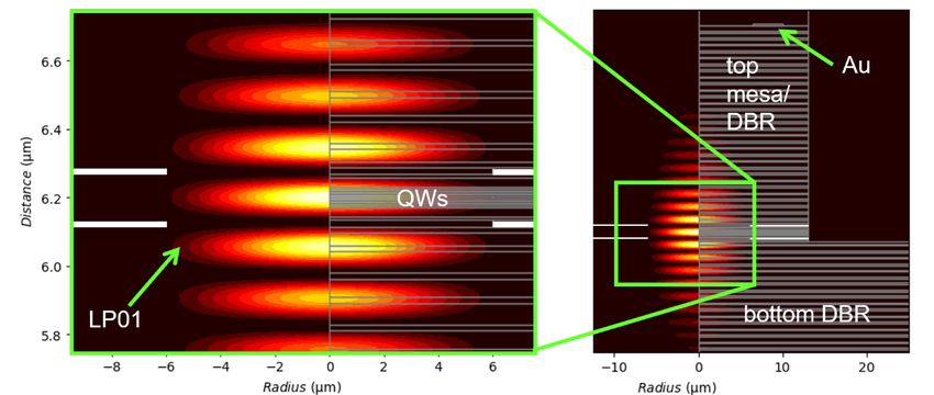
Materials 2021, 14, x FOR PEER REVIEW                                                                                                       8 of 18
   Materials 2021, 14, 397                                                                                                                      8 of 17

                                 the emission wavelength (980 nm), and c is the speed of light. We also plot, in Figure 5,
                                 the the
                                     LI slope   ηLI =η ΔL/=Δ∆L/
                                          LI slope           I (in∆IW/A)   for thefor
                                                                      (in W/A)      triple arraysarrays
                                                                                      the triple          withμm
                                                                                                   with ϕ~8      φ~8and   and μm.
                                                                                                                      µmϕ~13   φ~13For
                                                                                                                                    µm. theFor
                                                                                                                                            13 the
                                                       LI
                                 μm13 triple VCSEL      array,    η QE and ηLI peak at ~0.7 (unitless) and ~0.9 (W/A) at about I = 10
                                         µm triple VCSEL array, η QE and η LI peak at ~0.7 (unitless) and ~0.9 (W/A) at about
                                 mAI and
                                       = 10drop   to about
                                             mA and     drophalf     thesehalf
                                                                to about    magnitudes     at I ~70 mA.
                                                                                these magnitudes      at IFor
                                                                                                           ~70the
                                                                                                                mA.8 μm
                                                                                                                     Fortriple
                                                                                                                         the 8 VCSEL    array,
                                                                                                                                µm triple  VCSEL
                                 ηQE array,
                                      and ηLI  peak
                                             η QE andatη~0.65
                                                          LI  peak (unitless)
                                                                      at ~0.65 and   ~0.82
                                                                               (unitless)   (W/A)
                                                                                           and      at
                                                                                                 ~0.82 about
                                                                                                       (W/A)   I =
                                                                                                                 at5 mA
                                                                                                                    aboutand
                                                                                                                           I = drop
                                                                                                                               5 mA  to
                                                                                                                                    and about
                                                                                                                                          drop  to
                                 halfabout
                                       thesehalf
                                              magnitudes       at I ~45–50atmA.
                                                  these magnitudes            I ~45–50 mA.

                                     Figure
                                 Figure     5. Extracted
                                        5. Extracted      external
                                                      external     differential
                                                               differential     quantum
                                                                            quantum        efficiency
                                                                                      efficiency  (QE)(QE)
                                                                                                       andand  LI slope
                                                                                                           LI slope      efficiency
                                                                                                                    efficiency      versus
                                                                                                                                versus DC DC
                                 bias current for the 980 nm triple VCSEL arrays in Figure 3 with ϕ~8 and 13 μm.
                                     bias current for the 980 nm  triple VCSEL   arrays in Figure  3 with φ~8 and  13 µm.

                                     3.2. Emission Spectra and 2D Optical Mode Modeling
                                 3.2. Emission Spectra and 2D Optical Mode Modeling
                                           In Figure 6 (top), we plot the measured emission spectra of a triple 980 nm VCSEL
                                       In Figure 6 (top), we plot the measured emission spectra of a triple 980 nm VCSEL
                                     with φ~12 µm at a DC bias I = 3.5 mA (below threshold) and at I = 5.5 mA (above threshold).
                                 with ϕ~12 μm at a DC bias I = 3.5 mA (below threshold) and at I = 5.5 mA (above thresh-
                                     A common figure of merit for emission spectra (measured as a series of discrete points) is
                                 old). A common figure of merit for emission spectra (measured as a series of discrete
                                     the root-mean-square spectral width (in nm), which is calculated as follows [21–23]:
                                 points) is the root-mean-square spectral width (in nm), which is calculated as follows [21–
                                 23]:                         s
                                                                   n                                  n                            n
                                                                                                          P
                                                      ∆λ = ∑ (λi − λm )2 where λm = ∑ i λi , and Ptot = ∑ Pi ,                                       (1)
                                                                 i =1
                                                                                                         P
                                                                                                    i =1 tot                     i =1
                                    =                   −          where         =               ,       and          =           ,             (1)
                                     where n is the number of discrete measurement points, Pi is the optical power (in mW)
                                     at point
                                 where          i, λnumber
                                         n is the    i is the wavelength        at point i (in points,
                                                               of discrete measurement          nm), and        the(inoptical
                                                                                                          Pi isλm      nm) ispower
                                                                                                                               the mean      (average)
                                                                                                                                       (in mW)    at
                                     wavelength.       When    I =  5.5  mA,   we  get λ m = 984.05    nm   and   ∆λ   = 0.70
                                 point i, λi is the wavelength at point i (in nm), and λm (in nm) is the mean (average) wave- nm.
                                           We performed
                                 length. When      I = 5.5 mA,  two-dimensional
                                                                   we get λm = 984.05  cold
                                                                                          nmcavity
                                                                                              and Δmode λ = 0.70simulations
                                                                                                                  nm.         via the effective fre-
                                     quency    method       [24] as   implemented      in [25].  We    included
                                       We performed two-dimensional cold cavity mode simulations via the            near-field  images     for several
                                                                                                                                     effective  fre-
                                     example     optical   modes.      Each   allowed   mode   had    a corresponding
                                 quency method [24] as implemented in [25]. We included near-field images for several       wavelength,     which we
                                     plot asoptical
                                 example      straight    red lines
                                                       modes.    Each  in allowed
                                                                          Figure 6 mode
                                                                                    (top). For
                                                                                           hadexample,       the LP12wavelength,
                                                                                                a corresponding          mode (the only whichmodewenot
                                     labeled in Figure 6 (top)) is at λ = 983.47 nm. Comparing the measured emission spectra
                                 plot as straight red lines in Figure 6o(top). For example, the LP12 mode (the only mode not
                                     to the simulated modes, we find that (linearly polarized) modes LP01, LP11, LP21, LP02,
                                 labeled in Figure 6 (top)) is at λo = 983.47 nm. Comparing the measured emission spectra
                                     and others match well to the measured data. Note that our cold cavity simulations did not
                                 to the simulated modes, we find that (linearly polarized) modes LP01, LP11, LP21, LP02,
                                     include the impact of temperature (self-heating), spatial index of refraction variations due
                                 and others match well to the measured data. Note that our cold cavity simulations did not
                                     to injected carriers, spatial variations in QW gain, and more. In Figure 6 (bottom), we plot
                                 include the impact of temperature (self-heating), spatial index of refraction variations due
                                     the corresponding near field (surface) patterns for the LP01 and LP11 modes and for the
                                 to injected carriers, spatial variations in QW gain, and more. In Figure 6 (bottom), we plot
                                     simulated LP21, LP02, LP31, and LP42 modes. In Figure 7, we plot two-dimensional (2D)
                                 the corresponding near field (surface) patterns for the LP01 and LP11 modes and for the
                                     cross-sections of the simulated LP01 and LP11 modes. In future work, we plan to compare
                                 simulated LP21, LP02, LP31, and LP42 modes. In Figure 7, we plot two-dimensional (2D)
                                     measured and simulated near-field surface patterns.
                                 cross-sections of the simulated LP01 and LP11 modes. In future work, we plan to compare
                                 measured and simulated near-field surface patterns.
Electrically Parallel Three-Element 980 nm VCSEL Arrays with Ternary and Binary Bottom DBR Mirror Layers - MDPI
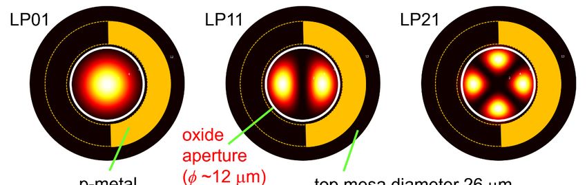
Materials 2021, 2021,
      Materials 14, x 14,
                      FOR 397PEER REVIEW                                                                                                              9 of 179 of 18

           Figure 6. (top) Measured spectral emission for a 980 nm triple VCSEL array with φ~12 µm and top mesa diameters of 26 µm,
     Figure  6. (top)
          at static    Measured
                    bias currents ofspectral
                                      I = 3.5 mAemission
                                                    (below for   a 980 nm
                                                             threshold) andtriple
                                                                             I = 5.5VCSEL
                                                                                     mA (above arraythreshold).
                                                                                                       with ϕ~12    μm
                                                                                                                  The   and top
                                                                                                                      vertical redmesa     diameters
                                                                                                                                   lines indicate   the of 26
     μm, at static  bias  currents  of  I  = 3.5 mA   (below    threshold)  and   I = 5.5  mA    (above    threshold).   The  vertical
          wavelengths of some of the simulated LP modes. (bottom) Simulated (cold cavity) two-dimensional (2D) near field (surface)     red  lines  indicate
     the wavelengths      of some
          modes (normalized         of theoptical
                                 resonant     simulated    LP modes.of(bottom)
                                                     field intensities)              Simulated
                                                                          any one VCSEL        in the(cold
                                                                                                       array.cavity) two-dimensional
                                                                                                              The array  includes 3.5 µm(2D)widenear
                                                                                                                                                  (and field
     (surface)
          3 µmmodes
                 from the(normalized      resonant
                            top mesa 1 edge)          opticalp-metal
                                                 top surface   field intensities)   of any one
                                                                       contacts, partially         VCSEL
                                                                                             removed     hereinfor
                                                                                                                 the array.
                                                                                                                   ease      The array
                                                                                                                        of viewing   (but includes   3.5 μm
                                                                                                                                           included in
     widethe
           (and   3 μm fromInthe
              simulations).      thetop    mesa 1 we
                                     simulation,    edge)   top surface
                                                        adjusted         p-metal
                                                                   the VCSEL   etaloncontacts,
                                                                                       to fit thepartially
                                                                                                   LP01 mode  removed    hereatfor
                                                                                                                 wavelength     I = ease  of viewing
                                                                                                                                    3.5 mA;   all other (but
     included   in the simulations).
          wavelengths                     In the simulation, we adjusted the VCSEL etalon to fit the LP01 mode wavelength at I = 3.5
                          followed naturally.
     mA; all other wavelengths followed naturally.
Electrically Parallel Three-Element 980 nm VCSEL Arrays with Ternary and Binary Bottom DBR Mirror Layers - MDPI
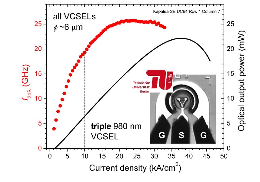
Materials 2021,2021,
     Materials  14, x14,
                      FOR397PEER REVIEW                                                                                                   10 of 10
                                                                                                                                                17 of 18

          Figure
     Figure       7. Simulated
             7. Simulated       two-dimensionalLP01
                            two-dimensional        LP01andandLP11
                                                              LP11 cold
                                                                    cold cavity
                                                                          cavitymodes
                                                                                  modes(normalized resonant
                                                                                          (normalized       optical
                                                                                                      resonant      field field
                                                                                                                optical    intensities) for a for
                                                                                                                                intensities)
          cylindrically symmetric   (rotated  2π about   the vertical line at radius = 0) 980 nm VCSEL with       µm    (corresponding
     a cylindrically symmetric (rotated 2π about the vertical line at radius = 0) 980 nm VCSEL with ϕ~12 μm (corresponding
                                                                                                            φ~12                           to to
          any of
     any one  onethe
                   of three
                      the three VCSELs
                            VCSELs    in in
                                         thethe triplearray
                                              triple   arrayininFigure
                                                                 Figure 6).
                                                                         6).

                                            As a sanity check, we used the equation in [26] to estimate (to first order) the φ for
                                          As a sanity check, we used the equation in mode
                                       the 12 µm triple VCSEL as follows. The estimated
                                                                                                 [26] tosize
                                                                                                          estimate    (to first order) the  ϕ for
                                    the 12 μm triple VCSEL as follows. The estimated       n      mode     (for
                                                                                                          size
                                                                                                                  a square aperture of io
                                                                                                              h(for  a square   aperture
                                                                                                                                         side
                                                                                                                                           of  side
                                       length b which we took as φ ≈ b is b ≈ sqrt 3π 2 /n2ave · 1/ (2π/λ1 )2 − (2π/λ0 )2
                                                                                                        
                                                                                                                                              .
                                    length b which we took as ϕ≈b) is ≈                        3 /          ∙ 1/ 2 /          − 2 /             . In
                                       In Figure 6 (top), the fundamental mode peak λ = 984.208 nm and the next higher-order
                                    Figure 6 (top), the fundamental mode peak λoo = 984.208 nm and the next higher-order
                                       mode peak λ1 = 983.980 nm when I = 3.5 mA. With the average optical cavity refractive
                                    mode
                                       indexpeak
                                               n ave λ≈1 =3.3,
                                                            983.980  nm
                                                               we find φ≈ when   I =nm
                                                                            11,997   3.5(~12
                                                                                         mA.µm).
                                                                                               WithAsthe   average
                                                                                                       a third  methodoptical  cavity refractive
                                                                                                                          to estimate   φ, we
                                    index          ≈   3.3,  we find  ϕ≈11,997   nm  (~12  μm).  As a third   method     to estimate
                                       performed selective thermal oxidation tests on several Kapalua test pieces as described        ϕ, we per-
                                    formed
                                       in [17]selective
                                               to determine thermal  oxidation tests
                                                                 the relationship      on several
                                                                                   between         Kapalua
                                                                                             oxidation  lengthtest
                                                                                                                andpieces   as described
                                                                                                                     oxidation             in [17]
                                                                                                                                  time. From
                                    to these
                                       determine
                                              data and  theour
                                                             relationship
                                                                knowledgebetween
                                                                            of the topoxidation   lengthwe
                                                                                       mesa diameters,     and   oxidation
                                                                                                              estimated    ourtime.
                                                                                                                               φ.    From these
                                    data and our knowledge of the top mesa diameters, we estimated our ϕ.
                                        3.3. Small-Signal Frequency Response
                                             We performed
                                    3.3. Small-Signal        small-signal
                                                         Frequency        modulation frequency response measurements primarily
                                                                    Response
                                        to determine the −3 dB bandwidth of our triple VCSEL arrays. As an example, in Figure 8,
                                           We performed small-signal modulation frequency response measurements primarily
                                        we plot, after correcting the data for the frequency response of the New Focus 25 GHz
                                    to bandwidth
                                        determine the     −3 dB bandwidth
                                                      photoreceiver,         of our|S21|
                                                                     the measured   triple(absolute
                                                                                           VCSEL arrays.   As an example,
                                                                                                    value magnitudes)   versusinfre-
                                                                                                                                 Figure
                                    8, we   plot,ofafter
                                        quency      a 980correcting the data
                                                          nm triple VCSEL    for with
                                                                           array the frequency
                                                                                      φ~6 µm at response  of the New
                                                                                                 DC bias currents of I =Focus   25 GHz
                                                                                                                        4, 8.5, and
                                    bandwidth photoreceiver, the measured |S21| (absolute value magnitudes) versus fre-
                                    quency of a 980 nm triple VCSEL array with ϕ~6 μm at DC bias currents of I = 4, 8.5, and
                                    18.5 mA (corresponding to bias current densities of about 4.7, 10.0, and 21.8 kA/cm2). We
                                    fit the measured |S21| data to the following equation [18]:
Materials 2021, 14, 397                                                                                                                                11 of 17

Materials 2021, 14, x FOR PEER REVIEW                                                                                                                  11 of 18
                                        18.5 mA (corresponding to bias current densities of about 4.7, 10.0, and 21.8 kA/cm2 ). We
                                        fit the measured |S21| data to the following equation [18]:
                                                                            v                                                
                                                                                             f R4                     1
                                                                             u
                                                                             u                                     1
                                                        |S21|
                                                     |S21          +·20
                                                          | = c=+ 20 log∙10 t            2                · ∙            2  (2)
                                                                                                                                 (2)
                                                                                f R2 − f−2 + (+         /2)2 1 +1 +f / f/p
                                                                                                  γ f /2π

                                        where cc (in
                                        where      (in dB)
                                                        dB) isis aa constant
                                                                     constant we  we useuse toto set
                                                                                                  set the
                                                                                                       the fitted
                                                                                                            fitted frequency
                                                                                                                    frequency response
                                                                                                                                   response to
                                                                                                                                             to the
                                                                                                                                                 the reference
                                                                                                                                                      reference
                                        level 00 dB
                                        level    dB atat the
                                                          the frequency
                                                               frequencyff == 0 Hz,   Hz, ffRR is
                                                                                                is the
                                                                                                    the relaxation
                                                                                                        relaxation oscillation resonance
                                                                                                                                    resonance frequency
                                                                                                                                                frequency (in(in
                                        GHz),
                                        GHz), γ       the damping
                                                 γ is the   damping(in     (inGHzGHzor  orequivalently
                                                                                           equivalentlyininns),        andfp fisp the
                                                                                                                  ns),and         is the parasitic
                                                                                                                                      parasitic    frequency
                                                                                                                                                frequency    (in
                                        (in GHz).
                                        GHz).        In Table
                                                 In Table    1, 1,wewe    listthe
                                                                       list     thefitting
                                                                                     fittingparameters
                                                                                               parametersand   andmeasured
                                                                                                                     measured bandwidths
                                                                                                                                   bandwidths for the 66 µm μm
                                        triple
                                        triple VCSEL
                                                VCSEL arrayarray corresponding
                                                                   corresponding to       to the
                                                                                              the measured
                                                                                                     measureddatadatain inFigure
                                                                                                                          Figure8.8.

                                        Figure 8. Measured
                                        Figure 8. Measured small-signal
                                                            small-signal modulation
                                                                         modulationfrequency
                                                                                      frequencyresponse
                                                                                                  response(|S21|)
                                                                                                              (|S21|) for
                                                                                                                       foraa980
                                                                                                                            980nm
                                                                                                                                nmtriple
                                                                                                                                   tripleVCSEL
                                        VCSEL
                                        array   array
                                              with φ~6with
                                                       µm ϕ~6  μm atcurrent
                                                           at direct direct (DC)
                                                                            current (DC)
                                                                                 bias     bias currents
                                                                                       currents I = 4, 8.5,I and
                                                                                                             = 4, 8.5,
                                                                                                                  18.5and
                                                                                                                       mA.18.5 mA.

                     Table 1. Extracted |S21|
                                         Fromfitting parameters
                                               the |S21|  data, for
                                                                 wethe Kapalua
                                                                    found  the triple
                                                                               −3 dB980 nm VCSEL modulation
                                                                                      small-signal with φ~6 µm.bandwidths (f3dB)
                                        for the triple array—i.e., the frequency f when |S21| = −3 dB in Equation (2). In Figure 9,
  DC Bias (mA)            J (kA/cm2 )     ~φ (µm) Each VCSEL          fR (GHz)       fp (GHz)       γ (ns)     f 3dB (GHz) DC L (mW)
                                        we plot f3dB as a function of DC    bias current (top plot) and as a function    of DC bias current
         4.0                  4.7                   6.0
                                        density (bottom    plot) for the  6 μm triple7.52671
                                                                      10.56701         VCSEL array.26.87444
                                                                                                       The maximum  13.0 bandwidth2.4is just
         8.5                 10.0       above 25 GHz6.0 for I ~18 to 20
                                                                      15.63646
                                                                        mA, a record 10.52691      38.10489
                                                                                        value for our  triple VCSEL 19.1arrays.   6.5
        18.5                 21.8                     6.0                   21.66922          13.91861         67.64717           25.2              15.1
                                        Table 1. Extracted |S21| fitting parameters for the Kapalua triple 980 nm VCSEL with ϕ~6 μm.
                                              From the |S21| data, we found the −3 dB small-signal modulation bandwidths (f 3dB )
                                         DC bias (mA) J (kA/cm2) ~ϕ (µm) each VCSEL fR (GHz) fp (GHz) γ (ns) f3dB (GHz) DC L (mW)
                                        for the triple array—i.e., the frequency f when |S21| = −3 dB in Equation (2). In Figure 9,
                                               4.0          4.7            6.0         10.56701 7.52671 26.87444    13.0         2.4
                                        we plot f 3dB as a function of DC bias current (top plot) and as a function of DC bias current
                                               8.5         10.0            6.0         15.63646 10.52691 38.10489   19.1         6.5
                                        density (bottom plot) for the 6 µm triple VCSEL array. The maximum bandwidth is just
                                              18.5         21.8            6.0         21.66922 13.91861 67.64717   25.2        15.1
                                        above 25 GHz for I ~18 to 20 mA, a record value for our triple VCSEL arrays.
                                              Next, in Figure 10, we plot f R and f 3dB versus (I − Ith )1/2 and extract two common
                                        dynamic VCSEL metrics: the D factor given by f R = D·(I − Ith )1/2 and the modulation
                                        current efficiency factor MCEF given by f 3dB = MCEF·(I − Ith )1/2 , where Ith is the threshold
                                        current. Thus, D = 5.69 GHz/(mA)1/2 and MCEF = 6.89 GHz/(mA)1/2 are the linear slopes
                                        in Figure 10 at the lower values of I.
Materials 2021, 14, 397                                                                                                                              12 of 17
Materials 2021, 14, x FOR PEER REVIEW                                                                                                        12 of 18

     Materials 2021, 14, x FOR PEER REVIEW                                                                                                    13 of 18
                                       Figure 9. Measured −3 dB small-signal modulation bandwidth (f 3dB ) versus direct current (DC) bias
                                  Figure 9. Measured −3 dB small-signal modulation bandwidth (f3dB) versus direct current (DC) bias
                                       I (upper plot) and versus J (lower plot) for a 980 nm triple VCSEL array with φ~6 µm.
                                  I (upper plot) and versus J (lower plot) for a 980 nm triple VCSEL array with ϕ~6 μm.

                                        Next, in Figure 10, we plot fR and f3dB versus (I − Ith)1/2 and extract two common dy-
                                  namic VCSEL metrics: the D factor given by fR = D·(I − Ith)1/2 and the modulation current
                                  efficiency factor MCEF given by f3dB = MCEF·(I − Ith)1/2, where Ith is the threshold current.
                                  Thus, D = 5.69 GHz/(mA)1/2 and MCEF = 6.89 GHz/(mA)1/2 are the linear slopes in Figure
                                  10 at the lower values of I.

                                        Figure
                                         Figure10.
                                                 10.Measured
                                                       Measured     −3 −
                                                                       dB3 bandwidth  (f3dB) (f
                                                                           dB bandwidth      and3dBrelaxation oscillation
                                                                                                    ) and relaxation      resonanceresonance
                                                                                                                       oscillation   frequencyfrequency
                                                                                                                                               (fR)     (f R )
                                        versus (I − I th)1/2 for
                                        versus (I − I )       1/2 the 980 nm  triple VCSEL    array   with ϕ~6 μm   in Figure
                                                                   for the 980 nm triple VCSEL array with φ~6 µm in Figure 9. 9.
                                                       th

                                        3.4. Data Transmission
                                            To demonstrate the potential of our triple arrays as sources for free-space optical
                                        communication, we performed large signal modulation data transmission experiments at
                                        room temperature on a triple VCSEL array with ϕ~6 μm, but across an OM1 multiple-
Materials 2021, 14, 397                                                                                                           13 of 17

                                  3.4. Data Transmission
                                          To demonstrate the potential of our triple arrays as sources for free-space optical
                                    communication, we performed large signal modulation data transmission experiments at
                                    room temperature on a triple VCSEL array with φ~6 µm, but across an OM1 multiple-mode
                                    fiber (MMF) patch cord (as we are not equipped for free-space measurements) as described
                                    in Section 2 via two-level pulse amplitude modulation (PAM-2) with a pseudorandom
                                    binary sequence (PRBS) of word length 27 − 1. With butt-coupling of the OM1 MMF (with
                                    a core diameter of 62.5 µm) directly on the φ~6 µm triple VCSEL array (where the center of
                                    each VCSEL emitting aperture lies 31.5 µm from the triple VCSEL centroid), we coupled
                                    at most ~44% of the array emission from each VCSEL into the fiber (neglecting surface
                                    reflection). For 100% coupling, we would need one or more lenses to focus the emission
                                    into the optical fiber. For free-space transmission across a room or across a street, we
                                    would similarly require a series of lenses. For a practical free-space optical communication
                                    system, we would seek purposely to detect only a fraction of the optical intensity in a given
                                    beam (of data), especially if we employ a conical beam to cover a large detection area with
                                    multiple photoreceivers.
                                          In Figure 11, we plot the negative logarithm (base 10) of the bit error ratio (BER) versus
                                    the received optical power for a DC bias I = 22 mA (J~25.9 kA/cm2 ) for bit rates of 30
                                    and 40 Gb/s. We first optimized the eye pattern for 40 Gb/s, recorded the 40 Gb/s and
                                    30 Gb/s eye patterns with zero attenuation (the inset images in Figure 11), and used the
                                    same settings for the subsequent BER test at 30 Gb/s. Interestingly, since we optimized the
                                    testing for 40 Gb/s, the received optical power for the 40 Gb/s data was smaller compared
                                    to that for the 30 Gb/s data when the −log10 (BER) was below 6. We recorded zero errors
                                    when we set the optical attenuation to 0 dB (over a period exceeding 30 s); therefore, we
Materials 2021, 14, x FOR PEER REVIEW                                                                                        14 of 18
                                    set the BER to 1 × 10⁻¹³ . At 40 Gb/s, we transmitted ≥1.2 × 1012 bits (≥9.3 billion         PRB
                                    sequences), and then recorded the BER. As a check, we repeated the BER tests over 2 h
                                    testing periods and found the resulting BER with zero attenuation unchanged.

                                  Figure 11. Bit error ratio (BER) versus received optical power for a 980 nm triple VCSEL array with
                                Figure
                                  φ~6 µm11.atBit
                                              30error
                                                 and 40ratio (BER)
                                                         Gb/s,  viaversus   receiveddata
                                                                    a back-to-back   optical   power fortest
                                                                                           transmission  a 980 nm triple
                                                                                                             across       VCSEL array fiber
                                                                                                                    OM1 multiple-mode
                                with  ϕ~6 μm    at 30 and  40 Gb/s, via  a back-to-back   data transmission  test across OM1
                                  (MMF) with two-level pulse amplitude modulation (PAM-2, nonreturn to zero) and a pseudorandommultiple-
                                mode fiber (MMF) with two-level pulse amplitude            modulation  (PAM-2,    nonreturn to zero) and a
                                  binary sequence (PRBS) of word length 27 − 1. We optimized the BER test settings for 40 Gb/s and
                                pseudorandom binary sequence (PRBS) of word length 27 − 1. We optimized the BER test settings
                                  used the same settings at 30 Gb/s (thus leading to the smaller received optical power at 40 Gb/s
                                for 40 Gb/s and used the same settings at 30 Gb/s (thus leading to the smaller received optical
                                  when
                                power atthe
                                          40BER
                                              Gb/sexceeds
                                                     when the 1× 10−exceeds
                                                               BER
                                                                     6 ). Inset images: eye patterns at 25, 30, and 40 Gb/s taken at the
                                                                              1 ×10⁻⁶). Inset images: eye patterns at 25, 30, and 40 Gb/s
                                  minimum     BER   (with zero added    optical
                                taken at the minimum BER (with zero added       attenuation).
                                                                                    optical attenuation).

                                4. Discussion
                                    Our 980 nm triple VCSEL arrays exhibited record combinations of bandwidth, optical
                                output power, and efficiency (WPE, ηLI, and ηQE); however, when are arrays a superior
Materials 2021, 14, 397                                                                                             14 of 17

                                      4. Discussion
                                       Our 980 nm triple VCSEL arrays exhibited record combinations of bandwidth, optical
                                 output power, and efficiency (WPE, η LI , and η QE ); however, when are arrays a supe-
                                 rior choice compared with single VCSELs for optical wireless communication or sensing
                                 applications? Consider the data in Figure 12, wherein we plot the −3 dB small-signal
                                 modulation bandwidth f 3dB versus the static (continuous wave) optical output power L for
                                 triple 980 nm VCSEL arrays with φ~6, 9, and 14 µm. We generated the plot by matching
                                 our measured f 3dB versus I data (as in Figure 9 (top)) to our static L versus I data. From the
                                 curves, we deduced that the maximum bandwidth of the 9 µm array (f 3dBmax ~24 GHz) is
                                 only slightly lower than the f 3dBmax (~26 GHz) for the 6 µm array, but the optical output
                                 power of the 9 µm array at f 3dBmax (L~35 mW) is more than double the optical output
                                 power (L~15 mW) at f 3dBmax for the 6 µm array. We may increase L to ~50 mW with our 14
                                 µm array, but with a reduced f 3dBmax of about 20 GHz.
                                       To be conservative (i.e., for reliable oxide aperture VCSEL operation), we could
                                 choose to limit the operating current density (J) for our arrays and our single VCSELs
                                 to ~10 kA/cm2 [27]. In Figure 12, we indicate the operating points where J~10 kA/cm2
                                 with green circles, and we find for the 6 and 9 µm arrays that the corresponding f 3dB is
erials 2021, 14, x FOR PEER REVIEW
                                 ~18–19 GHz but L is about threefold higher for the 9 µm array (~15 mW versus 5 mW)
                                 compared to L for the 6 µm array. As another reference point, we plot in Figure 13 f 3dB
                                 versus L for the same 9 µm triple VCSEL array and for a single reference VCSEL (fabricated
                                 from the same epitaxial material) with φ~16 µm.

                                      Figure 12. Extracted f 3dB versus static optical output power (L) for 980 nm triple VCSEL arrays with
                                     Figure     12. Extracted f3dB versus static optical output power (L) for 980 nm tripl
                                      φ~6 µm (blue circles), φ~9 µm (red squares), and φ~14 µm (magenta triangles). The green circles
                                     ϕ~6   μm (blue circles), ϕ~9 μm (red squares), and ϕ~14 μm (magenta triangles).
                                      indicate the points where the bias current density J = 10 kA/cm2 .
                                     indicate the points where the bias current density J = 10 kA/cm2.
                                            The total emitting area of the single 16 µm VCSEL and the total emitting area of the triple
                                      9 µm VCSEL array in Figure 13 are approximately equal (e.g., π·(16/2)2 ≈ 3·π·(9/2)2 )—a per-
                                             Thewould
                                      fect match    totalrequire
                                                            emitting
                                                                  φ~15.59 area
                                                                            µm forofthe
                                                                                      the  single
                                                                                        single      16 As
                                                                                               VCSEL).   μm    VCSEL
                                                                                                            a result       and the total e
                                                                                                                     (not surprisingly),
                                     triple 9 μm VCSEL array in Figure 13 are approximately 2equal (e.g., π·(1
                                      their f 3dB versus L data very closely overlap, although the triple array achieves a higher
                                      maximum optical output power. At the operating points where J~10 kA/cm , the single
                                     aVCSEL
                                        perfect andmatch
                                                     the triplewould
                                                               array arerequire       ϕ~15.59 μm
                                                                           (within experimental       for
                                                                                                  error) thethe   single
                                                                                                              same.   A keyVCSEL).
                                                                                                                             difference As a
                                      (betweentheir
                                     ingly),      the single
                                                          f3dBVCSEL
                                                               versus and Lthedata
                                                                               triple very
                                                                                      VCSELclosely
                                                                                              array) notoverlap,
                                                                                                         apparent inalthough
                                                                                                                       Figure 13 is the
                                                                                                                                     the trip
                                      far-field pattern, which, for the large-aperture single VCSEL without lensing or engineered
                                     higher
                                      placement  maximum          optical
                                                   and/or interaction   of theoutput     power.would
                                                                               VCSEL emitters,      At the
                                                                                                         likelyoperating       points
                                                                                                                take a donut shape   as wher
                                     single VCSEL and the triple array are (within experimental error) the s
                                     ence (between the single VCSEL and the triple VCSEL array) not appa
                                     the far-field pattern, which, for the large-aperture single VCSEL witho
higher maximum optical output power. At the operating points where J~10
                          single VCSEL and the triple array are (within experimental error) the same.
                          ence (between the single VCSEL and the triple VCSEL array) not apparent in
                          the far-field pattern, which, for the large-aperture single VCSEL without len
Materials 2021, 14, 397                                                                                        15 of 17
                          neered placement and/or interaction of the VCSEL emitters, would likely
                          shape as typically higher-order transverse modes dominate the emission at
                          currents    due to nonuniform current injection (i.e., current crowding near the
                           typically higher-order transverse modes dominate the emission at elevated bias currents
                          oxide
                           due toaperture
                                   nonuniform layers).
                                                current injection (i.e., current crowding near the edges of the oxide
                           aperture layers).

                           Figure 13. Extracted bandwidth f 3dB versus static optical output power (L) for a reference 980 nm
                          Figure   13. Extracted bandwidth f3dB versus static optical output power (L) for a refere
                           single VCSEL with φ~16 µm (black circles) and for a 980 nm triple VCSEL array with φ~9 µm (red
                          single  VCSEL with ϕ~16 μm (black circles) and for a 980 nm triple VCSEL array with
                           squares). Inset: the corresponding LIV curves. The emitting areas of the single VCSEL and the triple
                          squares).
                           VCSEL arrayInset:    the corresponding
                                         are approximately               LIV curves.
                                                              equal. The maximum         The
                                                                                  f 3dB for the emitting
                                                                                                single φ~16 areas of the
                                                                                                            µm VCSEL      single
                                                                                                                      is ~23 GHz. VCSEL
                          ple
                           TheVCSEL
                               maximum   array    are
                                           f 3dB for theapproximately      equal.
                                                         triple φ~9 µm VCSEL  arrayThe
                                                                                     is ~24maximum
                                                                                            GHz.         f3dB for the single ϕ~16 μm
                          GHz.   The maximum f3dB for the triple ϕ~9 μm VCSEL array is ~24 GHz.
                           5. Conclusions
                                We find that, for free-space optical communication, top-emitting electrically parallel
                           VCSEL arrays with small to medium aperture diameters become increasingly attractive
                           compared to larger-aperture single VCSELs as the required optical output power increases.
                           For large numbers of elements (~570 elements as in [28] for example), we anticipate
                           significant decreases in bandwidth for top-emitting arrays due to increased resistive and
                           capacitive losses. By neglecting far-field patterns and beam shaping (not investigated here)
                           at low to moderate optical output powers (about 50 mW or less), single VCSELs may suit
                           the application. However, for medium to high power optical wireless communication
                           and sensing, we believe that arrays are a superior choice. There remains plenty more to
                           investigate including optimized packaging schemes, substrate emitting variations of our
                           epitaxial designs, beam shaping/combining via novel array geometries and/or surface
                           lenses, bandwidth–power–efficiency trade-offs for large arrays (~37 or more elements), and
                           studies of the advantages of optically coupled and uncoupled VCSEL arrays for optical
                           wireless communication and sensing.
                                Whereas herein we investigated electrically parallel, optically uncoupled triple arrays
                           with φ~6 to 17 µm produced from our Kapalua epitaxial design, in previous work [18],
                           we investigated a three-element 980 nm VCSEL array with φ~7.5 µm produced from our
                           Ka’anapali epitaxial design. Our Ka’anapali epitaxial design is similar to our Kapalua
                           epitaxial design but with 14.5 top DBR periods (one fewer than Kapalua) and with Al-
                           GaAs/GaAs bottom DBR layers (i.e., not including AlAs binary layers in the bottom DBR).
                           For the two designs, within our experimental error, most key triple array results (Lmax ,
                           maximum f 3dB , D factor, MCEF, maximum error free bit rate, etc.) were nearly the same
                           for equal φ, indicating that the binary DBR layers (as expected) enable increased Lmax at
                           rollover compared to purely ternary DBR layers. As we increase the number of top-emitting
Materials 2021, 14, 397                                                                                                             16 of 17

                                   VCSEL elements, the heat dissipating advantages of the binary Kapalua design will likely
                                   more clearly emerge, although we believe clever packaging schemes are equally if not
                                   more important.
                                        We anticipate that our work will help lead to compact, low-cost, temperature-stable,
                                   and reliable lasers for 5G and 6G systems applications with flexible geometry and scalable
                                   optical output power (e.g., by increasing the number of lasing elements in an array). We
                                   work at 980 nm for convenience, whereas our results and conclusions apply equally well to
                                   VCSEL arrays emitting from the ultraviolet to well above 1550 nm. Wavelength selection
                                   for practical systems depends typically on the desired photodetector (e.g., 905–910 nm for
                                   shallow silicon charge coupled devices, 940 nm for silicon avalanche photodiodes (PDs),
                                   and 980 nm for InGaAs PDs), and eye safety, which may also depend on the required
                                   free-space beam shape, for example, a pencil beam versus a conical beam.

                                   Author Contributions: Conceptualization, N.H. and J.A.L.; methodology, N.H. and J.A.L.; software,
                                   N.H. and J.A.L.; validation, N.H. and J.A.L.; formal analysis, N.H. and J.A.L.; investigation, N.H. and
                                   J.A.L.; resources, N.H. and J.A.L.; data curation, N.H. and J.A.L.; writing—original draft preparation,
                                   N.H. and J.A.L.; writing—review and editing, N.H. and J.A.L.; visualization, N.H. and J.A.L.;
                                   supervision, J.A.L.; project administration, J.A.L.; funding acquisition, J.A.L. All authors have read
                                   and agreed to the published version of the manuscript.
                                   Funding: The German Research Foundation funded this work via the Collaborative Research
                                   Center 787.
                                   Institutional Review Board Statement: Not applicable.
                                   Informed Consent Statement: Not applicable.
                                   Data Availability Statement: The data presented in this study are available on request from the
                                   corresponding author.
                                   Acknowledgments: We gratefully acknowledge Maciej Dems from the Lodz University of Technol-
                                   ogy, Poland, for sending us computer programming snippets, thus enabling our cold cavity mode
                                   modeling via his PLaSK VCSEL modeling software.
                                   Conflicts of Interest: The authors declare no conflict of interest.

References
1.    Lascola, K.M.; Yuen, W.; Chang-Hasnain, C.J. Structural dependence of the thermal resistance of vertical cavity surface emitting
      lasers. In Proceedings of the IEEE LEOS Summer Topical Meeting: Vertical-Cavity Lasers, Montréal, QC, Canada, 11–13 August
      1997; pp. 79–80. [CrossRef]
2.    Larsson, A. Advances in VCSELs for communication and sensing. IEEE J. Sel. Top. Quantum Electron. 2011, 17, 1552–1567.
      [CrossRef]
3.    G˛ebski, M.; Wong, P.-S.; Riaziat, M.; Lott, J.A. 30 GHz bandwidth temperature stable 980 nm vertical-cavity surface-emitting
      lasers with AlAs/GaAs bottom distributed Bragg reflectors for optical data communication. J. Phys. Photonics 2020, 2, 035008.
      [CrossRef]
4.    Hoslin, P.; Haynes, C. What Is 6G Internet and What Will It Look Like? Available online: https://www.highspeedinternet.com/
      resources/6g-internet (accessed on 1 November 2020).
5.    Triggs, R. 5G mmWave: Facts and Fictions You Should Definitely Know. Available online: https://www.androidauthority.com
      /what-is-5g-mmwave-933631/ (accessed on 1 November 2020).
6.    NTT Docomo, Inc. 5G Evolution and 6G. Available online: https://www.nttdocomo.co.jp/english/binary/pdf/corporate/techn
      ology/whitepaper_6g/DOCOMO_6G_White_PaperEN_20200124.pdf (accessed on 1 November 2020).
7.    Chowdhury, M.Z.; Hossan, M.T.; Islam, A.; Jang, Y.M. A comparative survey of optical wireless technologies: Architectures and
      applications. IEEE Access 2018, 6, 9819–9840. [CrossRef]
8.    Chowdhury, M.Z.; Shahjalal, M.; Hasan, M.K.; Jang, Y.M. The role of optical wireless communication technologies in 5G/6G and
      IoT solutions: Prospects, directions, and challenges. Appl. Sci. 2019, 9, 4367. [CrossRef]
9.    You, X.; Wang, C.X.; Huang, J.; Gao, X.; Zhang, Z.; Wang, M.; Huang, Y.; Zhang, C.; Jiang, Y.; Wang, J.; et al. Towards 6G wireless
      communication networks: Vision, enabling technologies, and new paradigm shifts. Sci. China Inf. Sci. 2021, 64, 110301. [CrossRef]
10.   Ali, W.; Cossu, G.; Gilli, L.; Ertunc, E.; Messa, A.; Sturniolo, A.; Ciaramella, E. 10 Gbit/s OWC system for intra-data centers links.
      IEEE Photonics Technol. Lett. 2019, 31, 805–808. [CrossRef]
11.   Liverman, S.; Bialek, H.; Natarajan, A.; Wang, A.X. VCSEL array-based gigabit free-space optical femtocell communication. J.
      Lightwave Technol. 2020, 38, 1659–1667. [CrossRef]
You can also read