Enhanced hybrid optics by growing silver nanoparticles at local intensity hot spots
←
→
Page content transcription
If your browser does not render page correctly, please read the page content below
Nanophotonics 2019; 8(9): 1457–1464
Research article
Ivan Shutsko, Christian Michael Böttge, Jonas von Bargen, Andreas Henkel, Maik Meudt
and Patrick Görrn*
Enhanced hybrid optics by growing silver
nanoparticles at local intensity hot spots
https://doi.org/10.1515/nanoph-2019-0019 propagation. Dielectric optical systems are often charac-
Received January 21, 2019; revised March 12, 2019; accepted terized by long-range propagation yielding high-quality
March 13, 2019
resonators [1, 2]. On the other hand, plasmonics enables
strong confinement of light at the nanoscale. A combina-
Abstract: Silver nanoparticles (AgNPs) show an extraordi-
tion of both in one hybrid device can be highly beneficial.
nary strong interaction with light, which enables confine-
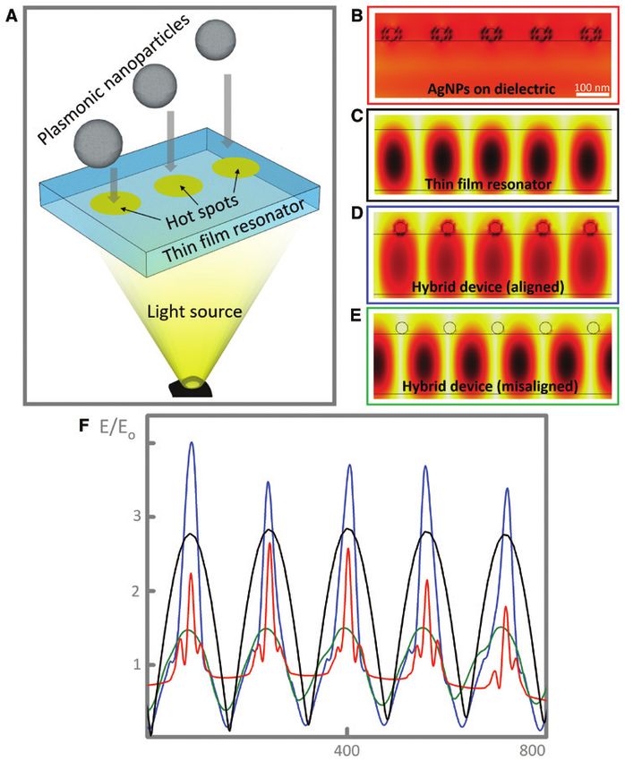
One example visualizing such benefits is shown
ment and field enhancement at the nanoscale. However,
in Figure 1. Silver nanoparticles placed on a dielectric
despite their localized nature, such phenomena are often
substrate and directly illuminated show sub-Abbe con-
sought to be exploited on a larger device length scale, for
finement and consequently field enhancement. This
example, in sensors, solar cells, or photocatalytic cells.
is depicted in red in Figure 1F, indicating the absolute
Unfortunately, this is often limited by strong absorption.
value of the electric field strength on the surface of a
One way to reduce these losses is to first focus light with
dielectric substrate and the corresponding cross section
low loss dielectric optics and then to place the AgNPs in
in Figure 1B. By placing the AgNPs on top of a thin film
that focus. Here, we present a clear experimental proof
resonator (Figure 1C and F, black curve), at the places
that growth of AgNPs from the liquid phase at a sub-
where the evanescent tails of the standing wave have
strate surface can be controlled by light. Violet light of
maximum electric field strength, this phenomenon can
405 nm and 1.5 W/cm2 is coupled into thin film resona-
be strongly enhanced (Figure 1D and F, blue curve) as
tors and locally focused at their surface. The AgNPs grow
the light interacting with the AgNPs can be collected on
at the focus position with sub-Abbe alignment accuracy.
a larger area. However, once the particles show only a
Numerical simulations confirm that this alignment causes
slight misplacement, the benefit is lost (Figure 1E and F,
an increased field enhancement within the AgNPs and is
green curve). In fact, the local field strength in case of
therefore expected to lead to an improved performance of
misalignment is even lower than for the pure AgNPs
the resulting hybrid devices.
on the dielectric substrate (Figure 1B and red curve in
Keywords: plasmonics; hybrid optics; resonators; silver Figure 1F).
nanoparticles. This example in Figure 1 shows the importance of
alignment of plasmonic nanoparticles in respect to the
thin film resonator. Such an aligned hybrid device in
1 Introduction Figure 1D, where plasmonic nanoparticles are placed on
the exact positions of maximum interaction with a thin
Hybrid optics is an emerging field enabling to combine the film resonator, will allow to locally confine an incoming
benefits of high localization with the benefits of low loss electromagnetic radiation harvested from a much larger
area. At the same time, it emphasizes the technological
challenge related to hybrid optics to produce such devices
*Corresponding author: Patrick Görrn, University of Wuppertal, in a cost-efficient way (Figure 1A).
School of Electrical, Information and Media Engineering, Chair of In particular, exact positioning of the plasmonic
Large Area Optoelectronics, Wuppertal, North Rhine-Westphalia, nanoparticles at the correct places of thin film resonators
Germany, e-mail: goerrn@uni-wuppertal.de or other focusing optical elements like lenses or tapered
Ivan Shutsko, Christian Michael Böttge, Jonas von Bargen, Andreas
waveguides will not only increase local field strength, but
Henkel and Maik Meudt: University of Wuppertal, School of
Electrical, Information and Media Engineering, Chair of Large Area
also often results in higher efficiency of hybrid devices. It
Optoelectronics, Wuppertal, North Rhine-Westphalia, Germany. also reduces the demand of rare and expensive coinable
https://orcid.org/0000-0002-3788-0318 (I. Shutsko) metals required for nanoscale confinement of visible light
Open Access. © 2019 Patrick Görrn et al., published by De Gruyter. This work is licensed under the Creative Commons Attribution 4.0
Public License.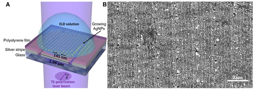
1458 I. Shutsko et al.: Enhanced hybrid optics by growing silver nanoparticles at local intensity hot spots Figure 1: The benefit of maximized interaction between the plasmonic nanoparticles and thin film resonator in a hybrid device. (A) Schematic illustration of the challenge related to hybrid optics in positioning of plasmonic nanoparticles at the hot spots of a large-area thin film resonator. (B) 20 nm AgNPs placed on a dielectric substrate. (C) Standing electromagnetic wave inside the thin film resonator. (D) 20 nm AgNPs placed on the thin film resonator at the maximum of evanescent field strength. (E) 20 nm AgNPs placed on the thin film resonator and shifted to the positions of minimum evanescent field strength. (F) Electric field strength on the surface of the dielectric with AgNPs on top (red curve), thin film resonator without AgNPs (black curve), aligned (blue curve) and misaligned (green curve) hybrid device. within large-scale optoelectronic devices. It is especially technology. In this paper, we have addressed that chal- desirable for the production of solar cells [3] or sensors lenge illustrated in Figure 1A. [4–7] and displays [8], where cost is of critical importance. The interaction of waveguide modes with plasmonic For the growing field of water splitting devices [9–11] nanostructures is studied by many research groups in the based on excitation of localized surface plasmon reso- field of hybrid optics. In recent studies [13–17], the focus was nance (LSPR) under solar radiation, this approach would put on the investigation of coupling between dielectric wave- also further reduce the amount of photocatalyst needed guide modes with plasmonically active nanoparticles such [12]. However, accurate optimum positioning of plasmonic as silver or gold nanoparticles (AgNPs or AuNPs), placed nanoparticles cannot be handled by state-of-the-art on top of a waveguide to explore the optical properties of
I. Shutsko et al.: Enhanced hybrid optics by growing silver nanoparticles at local intensity hot spots 1459
a hybrid device. In such hybrid devices, nanoparticles are characterization of the obtained nanopattern. First, the
excited through an evanescent tail of a propagating dielec- silver stripes with gaps of around 200 nm width were
tric waveguide mode. Depending on the waveguide geom- fabricated using a shadowing effect during thermal evap-
etry and the morphology of the metallic nanoparticles, this oration of silver at a certain angle onto the PDMS (polydi-
coupling leads to a fascinating modification of an optical methylsiloxan) blazed grating. Afterward, the stripes were
response of the waveguide through resonant scattering and transfer printed onto a glass substrate [42]. A polystyrene
absorption on NPs [13, 14], outcoupling through NPs [15], film spin-coated on top was flattened mechanically in
strong coupling regime [16], or energy transfer from guided order to ensure that the surface relief is not influenced
modes into plasmonic waveguide modes [17]. by the underlying silver gaps (supporting information,
Methods, influencing the growth of AgNPs, usually Figure S3A, B).
rely on the mechanical or chemical preparation of the The width of the gaps between the metal stripes and
substrate [18–31]. Hence, the substrate positions must the quality of the flattened polystyrene were characterized
be known, and the preparation often requires expensive by an atomic force microscope. A detailed description of
techniques such as electron beam or focused ion beam the sample preparation procedure can be found in the
lithography. On the other hand, nanoparticle trapping supporting information.
allows to control the positions of AgNPs with optical The second part of the experiment was the electroless
intensity gradients [32]. Unfortunately, only AgNPs that growth of the AgNPs on top of the polystyrene film from
are already grown to their maximum size can be influ- the liquid phase (ELD solution). The employed silver solu-
enced this way as the needed intensity strongly increases tion was prepared in accordance with [43] and was slightly
with lower particle diameter. Another drawback is the fact modified in order to increase the light sensitivity (50 drops
that the optical forces exist under light exposure only and of 6 v/v % ammonia solution were added additionally).
vary with the power of the incident light. In order to fix the The supporting information provides more details on elec-
particles, they must be welded to the subjacent film using troless AgNP growth.
even higher intensities, which further limits the applica- In the end, the ELD solution was cast on the polysty-
bility of nanoparticle trapping [33]. rene film and illuminated from the bottom glass side with
Nowadays, well-known bottom-up colloidal methods a CW laser with the wavelength of 405 nm and a power
allow producing sophisticated nanoparticles with perfect density of about 1.5 W/cm2. After 1 min of illumination,
control at the atomic scale [34–38]. On the other hand, using the drop of ELD solution was removed by nitrogen flow.
top-down approaches [37–39], the precise positioning and The resulting distribution of nanoparticles was analyzed
interparticle spacing could be reached [40, 41]. However, with a scanning electron microscope and an atomic force
a technique for bottom-up growing nanoparticles at the microscope (see supporting information).
desired places within a hybrid device has not been proposed.
In this paper, we will demonstrate a novel technique
for the fabrication of a hybrid device with maximized inter-
action between plasmonic nanoparticles and large-scale 3 Results and discussion
thin film resonator. We will show how to grow AgNPs from
liquid phase at the exact places of maximum intensity. Such As thin film resonator, we used a stack of a glass substrate
hot spots on the thin film resonator are formed at a reso- (ng = 1.47), silver stripes with 200 nm gaps and a period
nance condition. We utilize the absorption of light to start of 1.66 μm, and a polymer film on top (np = 1.62). Details
the growth mechanism from the atomic scale. As a conse- about the preparation are described in the methods above
quence, small light intensities can be applied and AgNPs and Supporting Information of this article (sections
are permanently fixed even at touchy films. We chose a thin “Blazed angle evaporation and transfer printing” and
film resonator produced by transfer printing and spin-coat- “Flattening of polymer film”). By illuminating the thin
ing to demonstrate the general use of our approach. film resonator (Figure 2A) from the glass bottom side with
a plane wave in TM polarization, surface plasmons are
excited propagating on both interfaces of the silver film
from the gap. On the other hand, by choosing TE polari-
2 Materials and methods zation, TE dielectric modes are excited at the gaps and
coupled into the polymer film. This way, the presented
The experiments were divided into three parts: prepara- structure of the thin film resonator is able to support both
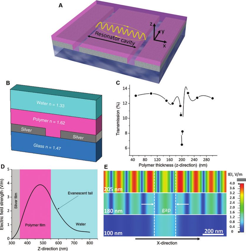
tion of a thin film resonator, AgNP growth on top, and delocalized surface plasmon waves and dielectric modes.1460 I. Shutsko et al.: Enhanced hybrid optics by growing silver nanoparticles at local intensity hot spots
Figure 2: Simulation of thin film resonator.
(A) Schematic illustration of the resonator cavity in polymer film. (B) Thin film resonator structure with water mimicking the ELD solution.
(C)Transmission of TE-polarized light (405 nm) through the thin film resonator at different thicknesses of the polymer film. (D) Evanescent
wave of the resonator mode. (E) 2D cut of absolute value of electric field strength distribution on the polymer film surface at its thicknesses
of 205, 180, and 100 nm (view from the surface side of the thin film resonator), the white dashed line indicates the area with a gap between
silver stripes.
In this work, we have focused on the resonant excitation because incident light is coupled into TE modes and guided
of TE dielectric modes in the polymer film. inside the polymer film forming a mode resonance. The
To analyze the optical properties of the resonator, a resonance is lost as soon as there is only a slight change of
numerical simulation (time and frequency domain solver the thickness of the polymer film, which can also be seen
of CST Studio Suite) is applied. The simulated structure is in the sharp drop of transmission in Figure 2C. The simula-
covered with water mimicking the ELD solution (electro- tions show that the resonance is also very sensitive to vari-
less deposition) needed for AgNP growth (Figure 2B). When ations of the gap width, even by a few percent.
the thin film resonator is illuminated with a TE-polarized The evanescent wave of the resonator mode in
plane wave at the wavelength of 405 nm, around 12–14% Figure 2D shows pronounced tails decaying over about
of the light is transmitted through, depending on the thick- 130 nm into the water (direction z). Accordingly, the
ness of the polymer film (Figure 2C). At a thickness of the electric field strength in the evanescent tail in water is
polymer film of around 205 nm, the transmission drops, three times higher than in an incident plane wave. TheI. Shutsko et al.: Enhanced hybrid optics by growing silver nanoparticles at local intensity hot spots 1461
evanescent wave amplitude varies harmonically with the of illumination is shown in Figure 3B. It confirms that
distance from the gap (direction x, Figure 2E). By decreas- growth of AgNPs was mediated at the places of maximum
ing the thickness of the polymer film, the resonance is evanescent field strength (Figure 2E).
lost and the corresponding strength of electric field in The 2D nanopattern consists of two types of lines: thick
evanescent tails drop dramatically. The evanescent wave lines with a period of 1.66 μm formed of coalescing AgNPs
on the surface of polymer film at the thicknesses of 180 above the gaps (see Figure 2A and dashed white lines in
and 100 nm is compared with a thickness of 205 nm Figure 2E) and thin lines between, with a period of around
(Figure 2E). The maxima of the plotted absolute values of 145 nm. The width of the thick lines corresponds to the width
electric field strength in the evanescent waves in Figure 2E of the gap (around 200 nm). The thin lines consist of AgNPs
show a distance of 145 nm. Therefore, it can be concluded with an average diameter of around 40 nm. The period of the
that the wavelength of the film mode is 290 nm. This value lines is 145 nm, which corresponds to half of the wavelength
is in good agreement with the wavelength of the wave of the simulated evanescent wave on the surface of the
propagating in the polymer film between silver and water polymer film λ0/(2 × neff), see Figure 2E. This feature size also
with an effective refractive index of 1.39, calculated using defines the resolution limit usually found in light-induced
the transfer matrix method. patterning. The fact that the lines are clearly distinguish-
The harmonically varying evanescent wave formed on able confirms sub-Abbe positioning accuracy of the AgNPs,
the surface of the thin film resonator serves as a driver for the which is explained by LSPR excitation. The number of the
nucleus formation and further plasmon-mediated growth of lines matches the simulated number of maxima shown in
AgNPs [44] from ELD solution. The proposed model of the Figure 2E. For a better illustration of areas with thick and
growth mechanism of AgNPs on the surface of polystyrene thin AgNP lines, we have marked them out with different
is described in detail in the supporting information. It has colors and performed a fast Fourier transform analysis of
been demonstrated before that the arrangement of AgNPs the highlighted areas with thin lines to determine the period
grown in a similar way but without focus is influenced by of the lines (see supporting information).
the parameters of the light source [43]. That has been inter- The AgNP growth rate above the gaps is higher
preted as a growth mechanism mediated by local intensity than for the particles between the gaps (Figure 3B).
variations. However, a direct control of the AgNP positions This observation is in agreement with the simulation
utilizing this phenomenon has not yet been reported. results in Figure 2E for the polymer film with 180 nm
To prove the idea that growth takes place at hot spots of thickness, where the evanescent field strength above
on the polymer film surface where the evanescent wave the gap is higher than throughout the entire surface
has the maximum value of electric field strength, the ELD area between the gaps. As it was predicted by the sim-
solution is cast on top of the 180 nm polymer film of the ulation, thickness variation of the polymer film has a
thin film resonator, which is kept under a CW laser irra- strong impact on the resonance behavior of our pre-
diation in TE polarization (Figure 3A). The scanning elec- pared structure. The thickness measurements show a
tron micrograph of the obtained nanopattern after 1 min deviation of 25 nm from the desired thickness of 205 nm.
Figure 3: Experimental creation of the optimized hybrid device by growing AgNPs at the local intensity hot spots of the thin film resonator.
(A) Schematic illustration of AgNP growth on top of the 180 nm polystyrene film of the thin film resonator. (B) Scanning electron micrographs
of the AgNPs on the polystyrene.1462 I. Shutsko et al.: Enhanced hybrid optics by growing silver nanoparticles at local intensity hot spots
Even such small thickness variations of ±10% cause sig- efficient confinement of the incoming light for the AgNPs
nificant changes in the simulated field distribution as with a diameter corresponding to LSPR. At the same time,
emphasized in Figure 2E. a small shift from the right position leads to strongly
To check the adhesion between grown AgNPs and decreased coupling between modes of thin film resonator
the polystyrene film, the structure was treated with a and AgNPs, which is shown in Figure S7A, B, C in the sup-
supersonic bath at room temperature. After 10 min, we porting information. Moreover, by examining a scattering
observed the partial removal of the particles from the cross section we observed a significant modification of the
places between the gaps. After 15 min, the thin lines were far-field scattering directions when AgNPs are shifted to
almost removed, whereas the thick lines above the gaps the optimized positions (Figure S7D).
remained almost unchanged (see morphology develop- The parameters enhanced in our hybrid device,
ment at the SEM micrographs in the supporting informa- absorption and scattering, depend not only on the align-
tion, Figure S6). This experiment supports our idea that ment of AgNPs on the hot spots but also on the shape
light exposure locally increases the adhesion of AgNPs and size of the AgNPs. For instance, the size of the AgNPs
on the substrate [45, 46] through plasmon-mediated pho- grown with the presented method is optimal for increased
tooxidation, and adhesion increases with the intensity of interaction with the incident laser beam. Therefore, the
the light confined at a hot spot. increased absorption and scattering cannot be unam-
According to Figure 1, the alignment of AgNPs at the biguously attributed to alignment using these devices. In
positions of maximum intensity should also lead to their order to experimentally prove the impact of alignment,
increased interaction with the incident light wave. While more selective parameters would be helpful. That is why
Figure 1 used a simplified resonator geometry, we now the decision was in favor of a different device, hybrid
probe the resonance behavior of the experimentally real- waveguide couplers. These show a more direct interaction
ized hybrid device consisting of the thin film resonator between two waves via interference, a mechanism that
with the AgNPs on top through numerical simulations of relies on the interplay of many AgNPs, and thus on align-
the near- and far-field optical properties. It is found that ment. These experimental results can be found in the sup-
the simulated hybrid device with AgNPs at the positions of porting information (section “Hybrid waveguide couplers
maximum interaction with the thin film resonator shows by optimized alignment of AgNPs”).
Figure 4: Scanning electron micrographs of AgNPs on 100 nm polystyrene film growing above the gaps.I. Shutsko et al.: Enhanced hybrid optics by growing silver nanoparticles at local intensity hot spots 1463
In our second set of experiments, we aimed to sup- References
press resonator TE modes in the polymer film by decreas-
ing the thickness from 180 to 100 nm where these waves [1] Poon JKS. Integrated ultra-low-loss resonator on a chip. Nat
can be neglected (Figure 2E). In this case, the resulting Photon 2018;12:255–6.
electric field on top of the polymer film is found above [2] Cai DP, Lu JH, Chen CC, Lee CC, Lin CE, Yen TJ. High Q-factor
the gaps. As predicted by the simulation in that case, we microring resonator wrapped by the curved waveguide. Sci Rep
2015;5:10078.
observed an alignment of the AgNPs on the surface of
[3] Alwater HA, Polman A. Plasmonics for improved photovoltaic
the polymer above the gaps only (Figure 4). No growth devices. Nat Mater 2010;9:205–13.
between the gaps is observed. This result also confirms [4] Peyskens F, Wuytens P, Raza A, Van Dorpe P, Baets R. Wave-
that AgNP growth between the gaps requires dielectric guide excitation and collection of surface-enhanced Raman
modes forming hot spots at the resonator (compare the scattering from a single plasmonic antenna. Nanophotonics
2018;7:1299–306.
case of 180 and 100 nm polymer thickness in Figure 2E).
[5] Wang H, Li H, Xu S, Zhao B, Xu W. Integrated plasmon-enhanced
The nanopatterning is observed on the entire area Raman scattering (iPERS) spectroscopy. Sci Rep 2017;7:14630.
of the laser spot (2 mm). The width of the grown lines [6] Cortés E, Xie W, Cambiasso J, et al. Plasmonic hot electron
varies between 200 and 220 nm, which corresponds to the transport drives nano-localized chemistry. Nat Commun
simulation of the near-field distribution on the dielectric 2017;8:14880.
surface above the gap. The diameter of the nanoparticles [7] Sánchez-González A, Corni S, Mennucci B. Surface-enhanced
fluorescence within a metal nanoparticle array: the role of sol-
stays in the range of 50–60 nm and could be varied by the
vent and plasmon couplings. J Phys Chem C 2011;115:5450–60.
used wavelength [43, 44, 47]. Furthermore, in our case, we [8] Hsu CW, Zhen B, Qiu W, et al. Transparent displays enabled by
observe a slight coalescence of nanoparticles, which can resonant nanoparticle scattering. Nat Commun 2014;5:3152.
be controlled by time and the concentration of silver ions [9] Xiao FX, Liu B. Plasmon-dictated photo-electrochemical
in the solution [48]. The surface tension has an impact on water splitting for solar-to-chemical energy conversion:
current status and future perspectives. Adv Mater Interfaces
the shape of the formed nanoparticle. The more hydro-
2018;5:1701098.
phobic the surface, the more the shape becomes spheri- [10] Warren SC, Thimsen E. Plasmonic solar water splitting. Energ
cal. Here, the shape is explained by a low surface energy Environ Sci 2012;5:5133–46.
of the polystyrene film (52 mN/m). [11] Lee J, Mubeen S, Ji X, Stucky GD, Moskovits M. Plasmonic pho-
toanodes for solar water splitting with visible light. Nano Lett
2012;12:5014–9.
4 Conclusion [12] Wei Q, Wu S, Sun Y. Quantum-sized metal catalysts for
hot-electron-driven chemical transformation. Adv Mater
2018;30:1802082.
In summary, we have shown that AgNPs are grown at local [13] Stuart HR, Hall DG. Enhanced dipole-dipole interaction
intensity focus spots. These spots were created with a thin between elementary radiators near a surface. Phys Rev Lett
film resonator produced by spin-coating and transfer print- 1998;80:5663.
[14] Quidant R, Girard C, Weeber JC, Dereux A. Tailoring the trans-
ing. Such facile scalable focusing structures could improve
mittance of integrated optical waveguides with short metallic
the efficiency of plasmon phenomena in low cost or even nanoparticle chains. Phys Rev B 2004;69:085407.
large area applications and, at the same time, reduce the [15] Arango FB, Kwadrin A, Koenderink FA. Plasmonic anten-
amount of plasmon or photocatalyst material needed. nas hybridized with dielectric waveguides. ACS Nano
However, usually with increasing focus, e.g., increasing 2012;6:10156–67.
quality factor, the sensitivity toward imperfections is also [16] Magno G, Fevrier M, Gogol P, et al. Strong coupling and vor-
texes assisted slow light in plasmonic chain-SOI waveguide
increased. In fact, in many practical cases, variations of
systems. Sci Rep 2017;7:7228.
the exact focus positions will have to be accepted. This is [17] Février M, Gogol P, Aassime A, et al. Giant coupling effect
where we anticipate the benefit of our method compared between metal nanoparticle chain and optical waveguide.
with other top-down methods. As the light of the focusing Nano Lett 2012;12:1032–7.
device directly controls the AgNP growth, it automatically [18] Baraldi G, Bakhti S, Liu Z, et al. Polarization-driven self-
organization of silver nanoparticles in 1D and 2D subwave-
enforces the creation of an optimized hybrid system.
length gratings for plasmonic photocatalysis. Nanotechnology
2017;28:035302.
Acknowledgments: This project has received funding
[19] Liu Z, Destouches N, Vitrant G, et al. Understanding the growth
from the European Research Council (ERC) under the mechanisms of Ag nanoparticles controlled by plasmon-
European Union’s Horizon 2020 research and innovation induced charge transfers in Ag-TiO2 films. J Phys Chem C
programme (grant agreement No. 637367). 2015;119:9496–505.1464 I. Shutsko et al.: Enhanced hybrid optics by growing silver nanoparticles at local intensity hot spots
[20] Eurenius L, Hägglund C, Olsson E, Kasemo B, Chakarov D. Grat- 30 − 200 nm and comparison of their optical properties. J Am
ing formation by metal-nanoparticle-mediated coupling of light Chem Soc 2010;132:11372–8.
into waveguided modes. Nat Photon 2008;2:360–4. [35] Wiley BJ, Wang Z, Wei J, Yin Y, Cobden DH, Xia Y. Synthesis
[21] Goutaland F, Colombier J-P, Sow MC, Ollier N, Vocanson F. and electrical characterization of silver nanobeams. Nano Lett
Laser-induced periodic alignment of Ag nanoparticles in soda- 2006;6:2273–8.
lime glass. Opt Express 2013;21:31789–99. [36] Xia Y, Xiong Y, Lim B, Skrabalak SE. Shape-controlled synthesis
[22] Wisser FM, Schumm B, Mondin G, Grothe J, Kaskelab S. Precur- of metal nanocrystals: simple chemistry meets complex phys-
sor strategies for metallic nano- and micropatterns using soft ics? Angew Chem Int Ed 2009;48:60–103.
lithography. J Mater Chem C 2015;3:2717–31. [37] Pelton M, Aizpurua J, Bryant G. Metal-nanoparticle plasmonics.
[23] Gangopadhyay AK, Krishna H, Favazza C, Miller C, Lasd Photon Rev 2008;2:136–59.
Kalyanaraman R. Heterogeneous nucleation of amorphous [38] Wiley B, Sun Y, Xia Y. Synthesis of silver nanostructures
alloys on catalytic nanoparticles to produce 2D patterned with controlled shapes and properties. Acc Chem Res
nanocrystal arrays. Nanotechnology 2007;18:485606. 2007;40:1067–76.
[24] Pang Z, Zhang X. Direct writing of large-area plasmonic [39] Gurevich EL, Gurevich SV. Laser Induced Periodic Surface Struc-
photonic crystals using single-shot interference ablation. tures induced by surface plasmons coupled via roughness.
Nanotechnology 2011;22:145303. Appl Surf Sci 2014;30:118–23.
[25] Kuznetsov AI, Evlyukhin AB, Gonçalves MR, et al. Laser fabrica- [40] Henzie J, Lee MH, Odom TW. Multiscale patterning of plasmonic
tion of large-scale nanoparticle arrays for sensing applications. metamaterials. Nat Nanotechnol 2007;2:549–54.
ACS Nano 2011;5:4843–9. [41] Merkel TJ, Herlihy KP, Nunes J, Orgel RM, Rolland JP, DeSimone
[26] Peláez RJ, Baraldi G, Afonso CN, Riedel S, Boneberg J, Leiderer JM. Scalable, shape-specific, top-down fabrication methods
P. Selective gold nanoparticles formation by pulsed laser inter- for the synthesis of engineered colloidal particles. Langmuir
ference. Appl Surf Sci 2011;258:9223–7. 2010;26:13086–96.
[27] Kaempfe M, Graener H, Kiesow A, Heilmann A. Formation of [42] Jakob T, Polywka A, Stegers L, et al. Transfer printing of
metal particle nanowires induced by ultrashort laser pulses. electrodes for organic devices: nanoscale versus macroscale
Appl Phys Lett 2001;79:1876–8. continuity. Appl Phys A 2015;120:503–8.
[28] Kiesow A, Strohkark S, Löschner K, et al. Generation of wave- [43] Polywka A, Tückmantel C, Görrn P. Light controlled assembly of
length-dependent, periodic line pattern in metal nanoparticle- silver nanoparticles. Sci Rep 2017;7:45144.
containing polymer films by femtosecond laser irradiation. [44] Langille MR, Personick ML, Mirkin CA. Plasmon-mediated
Appl Phys Lett 2005;86:153111. syntheses of metallic nanostructures. Angew Chem Int Edn
[29] Loeschner K, Seifert G, Heilmann A. Self-organized, grating 2013;52:13910–40.
like nanostructures in polymer films with embedded metal [45] Polywka A, Vereshchaeva A, Riedl T, Görrn P. Manipulating
nanoparticles induced by femtosecond laser irradiation. J Appl the morphology of silver nanoparticles with local plasmon-
Phys 2010;108:073114. mediated control. Part Part Syst Charact 2014;31:342–6.
[30] Bagratashvili VN, Rybaltovskii AO, Ilyukhin SS, et al. Laser- [46] Tanabe I, Tatsuma T. Plasmonic manipulation of color and
induced growth and self-organization of silver nanoparticles in morphology of single silver nanospheres. Nano Lett 2012;12:
colloidal polymers. Las Phys 2014;24:126001. 5418–21.
[31] Meudt M, Jakob T, Polywka A, et al. Metasurfaces: plasmonic [47] Callegari A, Tonti D, Chergui M. Photochemically grown silver
black metasurface by transfer printing. Adv Mater Technol nanoparticles with wavelength-controlled size and shape.
2018;3:1800124. Nano Lett 2003;3:1565–8.
[32] Bosanac L, Aabo T, Bendix PM, Oddershede LB. Efficient optical [48] José-Yacamán M, Gutierrez-Wing C, Miki M, Yang DQ,
trapping and visualization of silver nanoparticles. Nano Lett Piyakis KN, Sacher E. Surface diffusion and coalescence of
2008;8:1486–91. mobile metal nanoparticles. J Phys Chem B 2005;109:
[33] Maragò OM, Jones PH, Gucciardi PG, Volpe G, Ferrari AC. 9703–11.
Optical trapping and manipulation of nanostructures. Nat
Nanotechnol 2013;8:807–19.
[34] Zhang Q, Li W, Moran C, et al. Seed-mediated synthesis of Supplementary Material: The online version of this article offers
Ag nanocubes with controllable edge lengths in the range of supplementary material (https://doi.org/10.1515/nanoph-2019-0019).You can also read