Equivalent Circuit Model Separating Dissipative and Radiative Losses for the Systematic Design of Efficient Microstrip-Based On-Chip Antennas
←
→
Page content transcription
If your browser does not render page correctly, please read the page content below
1282                                                    IEEE TRANSACTIONS ON MICROWAVE THEORY AND TECHNIQUES, VOL. 69, NO. 2, FEBRUARY 2021

Equivalent Circuit Model Separating Dissipative and
  Radiative Losses for the Systematic Design of
   Efficient Microstrip-Based On-Chip Antennas
                Benedikt Sievert , Member, IEEE, Jan Taro Svejda , Member, IEEE, Jonathan Wittemeier,
       Nils Pohl, Senior Member, IEEE, Daniel Erni , Member, IEEE, and Andreas Rennings , Member, IEEE

   Abstract— This article presents a comprehensive method to                   contributions include the impedance mismatch between the
efficiently design capacitively enhanced resonant on-chip anten-               front end and antenna, the radiation efficiency of the antenna
nas using an equivalent circuit (EC) model instead of com-                     itself, and the spatial distribution of the radiated power, namely
putationally demanding full-wave simulations. To systemize the
design process by predicting the radiation efficiency, the input               the directivity. A desirable antenna design process considers
impedance, the current and voltage distributions, and the radi-                all the mentioned parameters and seeks for a (local) optimum
ation pattern of the antenna based on an EC, a method                          given the desired operation frequency, bandwidth, and antenna
to extract both dissipation and radiation mechanisms from                      gain with the constraint of a limited available chip area. Here,
full-wave simulation data is described and carried out. Based                  we will introduce an equivalent circuit (EC) model for a
on this separation of loss mechanisms, an EC-based antenna
optimization with respect to the radiation efficiency is conceivably           resonant microstrip antenna enhanced with series capacitances
possible. Additional to the EC, which enables this efficient                   to increase its radiation efficiency in the on-chip environment.
antenna optimization and increases the physical insight in the                 The on-chip environment usually inherits a very small distance
radiation mechanism, an analytical estimation of key antenna                   between the uppermost and lowermost metal layers, resulting
parameters, as the resonant length, is presented. The results                  in a limited radiation efficiency of frontside radiating on-chip
from the analytical calculations and the antenna parameters
calculated using the EC model are compared with full-wave                      antennas utilizing an on-chip ground plane [4] and, thus,
FDTD simulations and used to discuss the capabilities and                      a reduced gain [5], [6]. To solve this issue, the use of
limitations of the EC model. Finally, an on-chip antenna of the                series capacitances increasing the fringing fields and, thus,
considered type operating at 290–300 GHz and manufactured                      the radiation efficiency has been shown to be a promising
with silicon–germanium technology is used to verify the full-wave              measure [7]. Alternative approaches increase the distance
antenna simulations and the presented approach in general.
                                                                               between the antenna and the ground by an off-chip ground [8],
  Index Terms— Antennas’ theory and design, equivalent circuit                 which can be extended to a closed air cavity [9]. These
(EC), millimeter-wave and terahertz components, passive com-                   approaches can even achieve a moderate bandwidth by the use
ponent modeling, silicon–germanium (SiGe/Si) technologies.
                                                                               of fractal antennas [10] or multiband reception by combining
                                                                               antennas [11]. By use of dielectric resonators [12]–[14] or
                           I. I NTRODUCTION                                    high-dielectric superstrates [15], the outcoupling efficiency

T     HE need for highly efficient mm-wave on-chip
      antennas manifests in numerous applications, namely
high-resolution radar imaging [1], detailed material charac-
                                                                               can be increased, where at least the first ones are strongly
                                                                               dependent on proper alignment techniques [16]. At the cost of
                                                                               further fabrication effort, nonplanar antenna approaches can
terization [2], and high-data-rate communication [3]. A key                    achieve a drastically increased efficiency [17] and even high
parameter to increase the performance of the overall system                    gain [18]. Opposing to the here considered frontside radiating
is reducing the loss contributions of the transducer between                   on-chip antenna techniques, backside radiation through the
the front end and free space, namely the antenna. These loss                   semiconductor substrate and off-chip antennas [19] are also
                                                                               possible. Further details about the frontside and backside
  Manuscript received July 29, 2020; revised October 2, 2020; accepted
October 29, 2020. Date of publication December 24, 2020; date of cur-          radiating antennas and the corresponding antenna properties
rent version February 4, 2021. This work was supported by the Deutsche         can be found in [20].
Forschungsgemeinschaft (DFG, German Research Foundation) under Project            The EC model presented here aims to increase the physical
287022738—TRR 196 MARIE. (Corresponding author: Benedikt Sievert.)
  Benedikt Sievert, Jan Taro Svejda, Daniel Erni, and Andreas Rennings         insight into the radiation mechanisms of microstrip-based
are with the Center for Nanointegration Duisburg-Essen (CENIDE),               antennas and enable a fast optimization and design process.
Department of General and Theoretical Electrical Engineering (ATE),            It allows not only for the simplified description of complex,
University of Duisburg-Essen, 47048 Duisburg, Germany (e-mail:
benedikt.sievert@uni-due.de).                                                  electrodynamic radiation mechanisms by an EC but also for
  Jonathan Wittemeier and Nils Pohl are with the Institute of Integrated       the identification of radiating structures and their contribution
Systems, Ruhr University Bochum, 44801 Duisburg, Germany.                      to the antenna’s performance. The thorough extraction and
  Color versions of one or more figures in this article are available at
https://doi.org/10.1109/TMTT.2020.3040453.                                     separation of radiation and dissipation losses from full-wave
  Digital Object Identifier 10.1109/TMTT.2020.3040453                          simulations into EC models and the resulting prediction of
       This work is licensed under a Creative Commons Attribution 4.0 License. For more information, see https://creativecommons.org/licenses/by/4.0/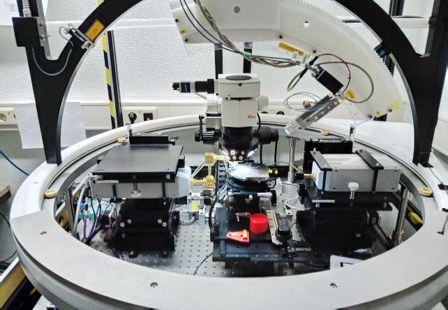
SIEVERT et al.: EC MODEL SEPARATING DISSIPATIVE AND RADIATIVE LOSSES                                                                                     1283

                                                                                Fig. 2. Schematic drawing of the capacitively coupled gap in (a) cross section
                                                                                and detailed stack information, (b) perspective view, and (c) top view with
                                                                                the dimensions used throughout.

                                                                                gaps. In general, neither the idea of radiating by microstrip dis-
                                                                                continuities nor the simplified modeling and resulting design
                                                                                guidelines of microstrip antennas are new [22], [23]. However,
Fig. 1. Realization example of a capacitively enhanced antenna utilizing four
capacitive gaps and a single-ended microstrip feedline. (a) Perspective view.   this article aims for a full EC description, allowing antenna
(b) Top view. (c) EC model assuming a zero-length feeding microstrip line       design based on circuit simulations. If the antenna is designed
(MSL).                                                                          as a periodic repetition of unit cells, a dispersion diagram
                                                                                analysis is possible [24], where it can be shown that, generally
input impedance, radiation efficiency, and directivity derived                  speaking, an increased number of gap capacitances and a
from circuit simulations are novel to the best of our                           smaller capacitive coupling have the tendency of decreasing
knowledge.                                                                      the antenna bandwidth [7]. In general, the capacitance of
   This article is organized as follows. Section II will introduce              a gap partly compensates the phase shift of a TL section,
the generic antenna design and a corresponding EC model                         which means that they can be used to increase the length
assembled out of building blocks. Based on the EC model,                        of the resonators while maintaining a λ/2-resonance. As a
Section III presents an analytical way to estimate the necessary                consequence, there exists the following tradeoff in the design
total antenna length and the approximate radiation efficiency.                  process. On the one hand, each capacitance results in a
To define the parameters of the EC elements, Section IV pro-                    further radiation contribution, which means that the radiation
vides and utilizes a method to extract the frequency-dependent                  efficiency can be increased by inserting gap capacitances
parameters based on full-wave simulations. Section V uses an                    into the resonator. On the other hand, each capacitance also
antenna design based on the analytical calculation to compare                   demands a TL section to counteract the phase compensation,
key antenna parameters predicted by the EC model to the                         and the losses introduced by the TL may overcompensate
outcome of a full-wave finite-difference time-domain (FDTD)                     for the efficiency gain achieved by the capacitive gap. In
simulation. Finally, in Section VI, the gain of an on-chip                      summary, the optimization process balances the efficiency
antenna based on the presented method will be measured and                      tradeoff between desirable capacitive gaps and necessary TL
compared with full-wave simulation results and the presented                    sections.
EC model in order to prove the modeling approach.                                  Fig. 1(a) shows the perspective, and Fig. 1(b) shows the top
                                                                                view of the antenna example, respectively, whereas Fig. 1(c)
                                                                                depicts the EC model built up by cascading different building
II. G ENERAL A NTENNA G EOMETRY AND I TS E QUIVALENT
                                                                                blocks. The building blocks of the model are explicitly labeled
               C IRCUIT R EPRESENTATION
                                                                                in both geometry and EC, but the antenna feeding is not part of
   The antenna presented in this article consists of cascaded                   the modeling. Since the EC reflects the geometrical outline of
building blocks, where the different building blocks, namely                    the antenna, the cascade of elements in the geometry is visual
the transmission line (TL) sections, the capacitive gap, and                    also in the EC. The antenna can be interpreted as the periodic
the end capacitance, will be characterized and transferred                      cascade of unit cells, and a unit cell of length UC is labeled
into EC models. An antenna example consisting of four                           as well. In this illustration, only the single-ended feeding is
capacitive gaps, which are embedded in a microstrip resonator,                  shown; however, a symmetric, differential feeding is feasible,
is depicted in Fig. 1. The microstrip antenna is built up in the                as it has been shown to increase the bandwidth and symmetrize
Infineon B11HFC silicon–germanium (SiGe) technology using                       the radiation pattern of microstrip antennas [25]. Fig. 2 labels
the uppermost aluminum and the lowermost copper layer as                        the dimensions of the antenna at a slice of the antenna,
the ground plane for the TL parts and overlapping, floating                     including the capacitive gap from different perspectives. The
copper patches for the capacitive gap, all of them embedded                     Swiss cheese structure, namely adding holes in the metal
in SiO2 . While the end capacitance built by the fringing fields                layer to fulfill density design rules of the SiGe technology,
of the microstrip line is the main radiation contribution of ordi-              applied to the floating layer of the capacitive gap is not
nary patch antennas [21, p. 835], this antenna mainly radiates                  depicted in Figs. 1 and 2 for reasons of clarity; however, it is
by the discontinuity in the TL introduced by the capacitive                     included in every simulation. Thus, the modeling is expected to
1284                                                     IEEE TRANSACTIONS ON MICROWAVE THEORY AND TECHNIQUES, VOL. 69, NO. 2, FEBRUARY 2021

                                  TABLE I
             D IMENSIONS OF THE A NTENNA G IVEN IN F IG . 2

                                                                                 Fig. 4. EC model of the capacitive gap based on (a) physical interpretation
                                                                                 and (b) conversion to series elements to ease further analytical calculations.

                                                                                 Fig. 5. EC model of the homogenized infinitesimal small TL, including
                                                                                 both the elements of the right-handed TL and the series representation of the
                                                                                 capacitive gap from Fig. 4.

                                                                                 antenna designs, which can be used as starting values for the
                                                                                 circuit simulation-based antenna design process.
Fig. 3. EC models of the cascaded building blocks utilized, namely (a) TL
of infinitesimal length dz, (b) its representation by the length, the complex      III. A NALYTICAL M ODEL OF H OMOGENIZED A NTENNA
propagation constant, and characteristic impedance, and (c) capacitive gap and
(d) end capacitance.                                                                In this section, the analytical estimation of the necessary
                                                                                 total antenna length tot for a half-wavelength current distri-
                                                                                 bution and resulting antenna efficiency is derived. The idea
represent the fabricated chip satisfying the restrictions of the                 behind this approach is converting the unit cell consisting of
fabrication process. All corresponding dimensions are given                      both a TL [see Fig. 3(b)] and the capacitive gap [see Fig 3(c)]
in Table I.                                                                      into a homogenized TL model, neglecting the influence of
   The detailed EC models of the building blocks, including                      the fringing fields at the end of the resonator, namely the
the nomenclature of the circuit elements, are depicted in Fig. 3.                end capacitance. It should be noted that the homogenization,
Here, the resistances or conductances corresponding to a dissi-                  which is in principle comparable to [24, p. 79], neglects
pative loss mechanism are highlighted by the index D, whereas                    the influence of the actual discrete placement. The effect
the radiation contributors are highlighted by the index R. In                    of this simplification will be discussed in Section V. As
contrast to earlier modeling of microstrip gaps [26], the gap                    this calculation only aims for the half-wavelength resonance,
utilized here is modeled as a simple series admittance instead                   the desired resonance frequency f 0 and the corresponding
of a -equivalent due to the dominant series capacitance.                        angular frequency ω0 are considered here.
Furthermore, it is defined with zero geometrical length instead                     First, the finite number of capacitive gaps Ncap is distributed
of its physical extend [27], meaning that the reference plane                    along the antenna length tot in a homogeneous, thus equidis-
for incoming and outcoming waves is coincident at the center                     tant manner representing quantitatively the original discrete
of the gap. For the gap conductance, the separation of power                     distribution of gaps. Since the capacitive gap is a series
radiated into free space and into surface waves [28] is not                      element, its shunt-representation will be transformed into a
carried out, as the substrate is electrically thin. If a thicker                 series representation (see Fig. 4) easing further calculations.
substrate with a significant surface wave loss was used, this                    Second, these series elements will then be transformed into an
should be considered as an additional loss in the modeling                       element per unit length by distributing them along the length
of the EC and in the extraction process. The end capacitance                     tot /Ncap [24, p. 82]. The transformation from shunt to series
could be modeled by an extension length [29]; nevertheless,                      elements is equal for G R and G D and analogous for Cgap
the separation into an own capacitance and conductance eases                     according to
building up the EC out of building blocks. By these choices,                                                                    2
both capacitances are represented in the EC as a concentrated                                            (G R + G D )2 + ω0 Cgap
                                                                                                     =
                                                                                                     C                                          (1)
element; and the phase shift associated with such an element                                                       ω02 Cgap
is only defined by its impedance and the environment that it                                                       G R/D
is embedded in, but not by wave-propagation. This eases the                                      R/D =
                                                                                                 R                              2 .           (2)
definition of the EC, as each TL has the length UC regardless                                           (G R + G D )2 + ω0 Cgap
of the length of the capacitive gap.                                                The series elements are denoted by a tilde in order to
   Section III will simplify the EC representation by approx-                    distinguish them from the shunt elements, and the resulting
imations in order to give closed formulas enabling initial                       homogenized EC is depicted in Fig. 5. Here, the series path
SIEVERT et al.: EC MODEL SEPARATING DISSIPATIVE AND RADIATIVE LOSSES 1285
of the TL contains both radiation and dissipation losses, The voltage and current along with the open-ended TL, given
as well as the phase shift of the capacitive gap. To con- by [33, pp. 60], can be used to calculate the loss contribution.
sider the phase shift per unit cell caused by the series To simplify the calculation, it is assumed that tot fulfills (9),
capacitance, an effective series inductance per unit length which means that the half-wavelength resonance results in an
consisting of both the homogenized gap capacitance and integration of the phase angle ϕ over the antenna length with
the inductance per unit length is calculated in accordance the integration bounds 0 ≤ ϕ ≤ π. This means that each series
with [24, p. 76] to gap,R
element contributes to radiation (R R and R
) or dissipation
(R D and Rgap,D ) according to
jωL TL +
Ncap
tot Ncap
L eff = L TL −
jωC
= (3) π
2|V0+ |2
jω
ω2 C tot
PSer = RSer sin2 (ϕ)dϕ. (12)
0 Im{γUC }|Z UC |2
which can be used with the following abbreviative variables:
In the same way, each shunt element contributes to radiation
G TL = G R + G D (4) (G R ) or dissipation (G D ) according to
RTL = R R + R D and (5) π
2|V0+ |2
N PShunt = G Shunt cos2 (ϕ)dϕ. (13)
= cap R
R gap,D
gap,R + R (6) 0 Im{γUC }
tot
Both integrations result in the same expressions except for
to calculate both the complex propagation constant and the
the term |Z UC |2 , which represents the squared ratio of
characteristic impedance of the homogenized model
traveling-wave voltage to current, thus enabling a comparison
of power loss of shunt and series elements. The radiation effi-
γUC, hom = G TL + jωCTL
RTL + jωL eff
+R (7) ciency, dividing the radiated power by all power contributions,
can be written as
RTL +R + jωL eff
Z UC, hom = . (8) gap,R
R
Ncap
G TL + jωCTL tot |Z UC |2 + G R
ηRad = . (14)
gap,R
+R gap,D
The length tot necessary to achieve a λ/2-resonance (total R Ncap R +R
+ |ZR UC |2D + G R + G D
tot |Z UC |2
phase shift of π) can be estimated by
π As will be shown later, the radiation contributions of the TL
tot = (9) are negligible (R R ≈ 0 and G R ≈ 0), and thus
| Im{γUC, hom }|
gap,R
R
Ncap
and the imaginary part of the propagation constant can be tot
approximated by the phase constant of the lossless unit cell ηRad ≈ (15)
gap,R
R gap,D
+R
Ncap
+ R D + |Z UC |2 G D
tot
Ncap
Im{γUC, hom } ≈ ω0 CTL L TL − 2 (10) can be used. In Section IV, the extraction of the EC parameters
tot
ω0 C
will be explained in detail. This enables the analytical calcula-
where the effective inductance from (3) has been inserted. tion of a capacitively enhanced antenna based on the equations
If (10) is plugged in (9), the result is a quadratic equation with presented within this section and allows for a comparison to
respect to tot , which can be solved to only positive lengths to full-wave simulations to prove both the calculations and the
EC model.
Ncap 1 2
Ncap π2
tot = 2
+ + . (11)
2ω0 C L TL ω0 4ω0 C 2 2 L TL
2 CTL L TL
IV. E XTRACTION OF F REQUENCY-D EPENDENT
This length can be used to estimate the total length of a E QUIVALENT C IRCUIT PARAMETERS
capacitively enhanced microstrip antenna with a number of To enable not only the extraction but also the physical
Ncap capacitive gaps if the inductance and capacitance per interpretation of EC elements, each EC element is extracted
unit length L TL and CTL
of the TL, as well as the capac- with arbitrary frequency dependence, which means that the
itance of the gap C, are known. As the gap investigated data sets of different frequencies will be extracted separately.
here is mostly capacitive, which means that radiation and Even though this allows, in general, for element values with
dissipation conductances are much smaller compared with the fluctuations over frequency, one would expect parameters
susceptance, one can assume that C ≈ Cgap , which means with physically sound frequency dependencies. If expected
that the length estimation can be carried out even without frequency dependence will be confirmed, future extraction
the extraction of radiation and dissipation losses. The TL processes could reduce the number of extraction points by
parameters can be estimated by any of the available analytical assuming this frequency dependence, as long as nonresonant
equations [29]–[32]. building blocks are characterized. Otherwise, the EC model
Finally, assuming a resonant current distribution and know- needs to be expanded to model, e.g., the inductance of
ing the dissipative and radiative EC elements from Fig. 5, the capacitive gap. The extraction methods applied to the
the radiation efficiency of the antenna can be estimated as different building blocks, i.e., the TL section, the capacitive
well. In this case, the radiation by the end capacitances and gap, and the end capacitance, are presented in the following.
the discrete placement of the gap capacitances are neglected. All of them utilize a combination of port-based parameters
1286                                                      IEEE TRANSACTIONS ON MICROWAVE THEORY AND TECHNIQUES, VOL. 69, NO. 2, FEBRUARY 2021

Fig. 6. Schematic drawing of the TL with (a) near-field recording box for the
calculation of loss and radiation contributions and (b) radiated electric field
in azimuthal direction caused by an applied voltage (blue) and the radiated
electric field in elevation direction caused by a current (red).

(e.g., Z -, Y -, and S-parameters) and integrals over near-field
data (e.g., power flow) to model the correct impedance
behavior while separating the different loss mechanisms.
This extraction of different loss parameters is the essential
advantage over the design equations for microstrip lines, e.g.,
from [29].
                                                                                  Fig. 7. Normalized EC elements of the TL. (a) Elements of the series path.
A. Transmission Line Parameters                                                   (b) Elements of the shunt path. All elements are normalized to their respective
                                                                                  values at f N = 300 GHz, which are given in Table II.
   As indicated in Fig. 3(a), the EC of the TL is characterized
by six elements, which depends, in general, on the geometry
                                                                                  be integrated over the areas corresponding to dielectric ( Adiel )
and material properties. Although the elements within the EC
                                                                                  or conducting (Acond ) media according to
assume an infinitesimal small piece of TL, the extraction is
carried out based on a finite geometrical length TL . In a                                                     1
full-wave FDTD simulation, a TL of length 1000 μm in the                                              Pcond =                  σ E2 d A                  (16)
                                                                                                                 2     Acond
z-direction is excited at one side. The TL guides the excited                                                    1

wave into a perfectly matched layer (PML), assuring that there                                         Pdiel   =               ωε E2 d A.              (17)
                                                                                                                 2     Adiel
exist only traveling and no standing waves. Thus, the input
impedance at the exciting port is equal to the characteristic                     In such a way, both losses per unit length can be divided by the
impedance Z TL of the TL, as the PML represents an ideal                          squared absolute current or voltage along the line to calculate
match. Two reference planes with a distance of 350 μm are                         the corresponding dissipation resistance R D and conductance
used to measure the traveling wave voltage and current, result-                   G D representing the conductor loss and the dielectric loss,
ing in frequency-dependent phase and attenuation information                      respectively. Furthermore, Fig. 6(b) shows the electric field
along the 350-μm long part of the TL, which, in combination,                      components that are assumed to be the dominant ones given
can be related to the complex propagation constant γTL . For the                  either a shunt voltage (E ϕ , drawn in blue) or a series current
detailed assessment of dissipation and radiation contributions,                   (E θ , drawn in red) as a radiation source. The total radiated
the near-field data need to be incorporated to extract the                        power is assigned to voltage- and current-driven radiation
EC elements related to the different loss mechanisms. In                          sources based on the ratio of power corresponding to the E ϕ
Fig. 6(a), the near-field recording box calculating the incident                  and E θ radiations, respectively. Finally, these weighted parts of
and transmitted power guided by the TL at the red and                             the radiated power are related to a loss integral of the squared
blue surfaces, respectively, is shown. The radiated power in                      absolute current or voltage to calculate the radiation resistance
the different directions (y+, x±) is evaluated at the gray                        R R and conductance G R . Since the propagation constant of
surfaces, and the difference between the incident power and                       the TL is already known, the evaluation of the loss integral is
the transmitted/radiated power is equal to the dissipated power                   straightforward.
in the TL section. After calculating the power balance of this                        To find a suitable EC model considering the different
near-field recording box based on the Poynting theorem [33,                       abovementioned parameters, a genetic algorithm representing
p. 26], the relation of radiated to dissipated power is known. As                 the EC elements by gray-coded parameters [35, p. 100] has
the EC differentiates between voltage driven and current driven                   been used to determine the EC with the best value of the fitness
loss mechanisms, namely conductances and resistances, both                        function, where the fitness function is a weighted sum of
the radiation and the dissipation losses need to be separated.                    the relative deviations of propagation constant, characteristic
The dissipative loss along the TL can occur due to losses                         impedance, and loss contributions between the circuit and
within
√       the conductor, which increases roughly proportional to                    full-wave simulation. As stated earlier, this optimization is
   f [34], and due to the losses within the dielectric, which                     carried out for each frequency independently. Fig. 7 represents
are expected to be proportional to f , according to a constant                    the extracted EC elements normalized to their respective value
tan δ. To separate both dissipative mechanisms, the volumetric                    at f N = 300 GHz. In this way, different units and orders
power loss density within the cross section of the TL needs to                    of magnitude can be compared concerning their frequency
SIEVERT et al.: EC MODEL SEPARATING DISSIPATIVE AND RADIATIVE LOSSES                                                                              1287

                            TABLE II
            EC E LEMENTS OF THE TL AT f N = 300 GHz

                                                                       Fig. 8. Schematic drawing of (a) capacitive gap in a perspective view and
                                                                       (b) end capacitance with recording box for the calculation of loss and radiation
dependence. The normalizing element values at 300 GHz are              contributions.
given in Table II. The reactive and dissipative elements can
also be extracted from a quasi-static 2-D FEM simulation
and are given for comparison. In addition, the values cal-
culated analytically by Owens [32] are listed there. Here,
extracted elements are in good agreement with the FEM
simulation and the analytical calculations. Looking at Fig. 7,
different frequency dependencies can be observed. To guide
the interpretation, usual dependencies on the frequency are
plotted as gray thick lines in the background. Concerning the
most dominant elements of the TL, namely its capacitance
and inductance per unit length, both behave extraordinarily
constant with respect to frequency. The radiative elements
                                                                       Fig. 9. EC elements for the capacitive gap extracted from the setup depicted
show minor undulations but follow, in general, the ∝ f 2               in Fig. 8(a) for both widths w f ∈ {27.5 μm, 33 μm}.
curve in a good agreement. From the analytical derivation
in [22], one would expect for a lossless TEM-line no radiation
contribution at all. However, the incorporation of losses yields       of the near-field recording box [see Fig. 8(a)]. With the TL
problems, as any source in an infinite distance would need             parameters extracted earlier, the dominant reactive part Cgap
to impress infinite currents yielding radiation contributions.         can be extracted by deembedding the two-port parameters by
In [28], it is stated that, even though a uniform line radiates        a distance of 175 μm per side.
power, nevertheless, the loss due to radiation would be much              To calculate the radiative and dissipative conductances,
smaller compared with the dissipative loss. This consistently          G gap,R and G gap,D , the radiated and dissipated powers contri-
fits the extracted radiation contributions that are orders of          butions by both the TL and capacitive gap inside the recording
magnitude smaller compared with the dissipative losses. The            box are extracted from the simulation. At the red and blue
dominant losses corresponding to conductor loss and dielectric         faces of the near-field recording box (see Fig. 8), the power
loss follow precisely the expected behavior; namely, the losses        flow along the TL needs to be separated from the radiated
within the√dielectrics are ∝ f , and the conductor losses              power of the discontinuity by accessing the voltage and current
follow the f -proportionality [34]. For future extractions, it is      at the reference planes. The difference of the power guided
obvious that similar structures can be analyzed only based on          by the TL (Pin , Pout ) and the power flow calculated by the
the reactive and dissipative elements, which can be calculated         near-fields at the reference planes (P,±z ) is associated with
by well-documented formulas per se [29], and the radiative             the outwards pointing radiation in the ±z-direction (PRad,±z )
elements of the TL can be neglected.                                   according to
                                                                                               P,z+ = −PRad,z+ + Pin                            (18)
B. Capacitively Coupled Gap
                                                                                               P,z- = +PRad,z- + Pout .                         (19)
   The procedure of extracting the EC elements for the capac-
itively coupled gap is comparable to the previous extraction,             All other radiation contributions can be directly extracted
but, here, the EC element is only a series element and,                from the remaining faces of the near-field recording box. From
thus, only dependent on the current. In general, the radia-            a circuit simulation, the dissipation and radiation contributions
tion conductance has been derived analytically for generic             of the TLs can be calculated and used to calculate the radiation
discontinuities in [36] however, more complicated structures,          and dissipation contributions of the capacitive gap. By utilizing
as presented here, might justify the extraction out of full-wave       the circuit simulation, the EC elements, G gap,R and G gap,D ,
simulations. Within this publication, two different overlapping        can be determined from the radiated and dissipated powers,
areas are extracted as examples, namely w f = 27.5 and                 respectively. The extracted EC elements in dependence on the
33 μm. In the FDTD simulation, the capacitive gap is located           frequency are depicted in Fig. 9. From the extracted elements,
at the center of the already known TL. Two reference planes            one can see that the capacitance is almost constant, whereas
with a distance of 350 μm centered around the capacitive gap           both dissipation and radiation losses increase with frequency.
are used for recording two-port parameters, namely the current         The capacitive gap becomes a good radiator above 300 GHz,
and voltage assuming a quasi-TEM behavior, and near-field              where the ratio of radiation conductance to dissipation con-
parameters, namely the power flow through the respective side          ductance peaks. This ratio could be interpreted as the intrinsic
1288                                                     IEEE TRANSACTIONS ON MICROWAVE THEORY AND TECHNIQUES, VOL. 69, NO. 2, FEBRUARY 2021

                                                                                 extracted EC parameters, an EC model can be built up and
                                                                                 evaluated. All TL sections are of length TL = tot /5 ≈
                                                                                 119 μm, and the general EC is already depicted in Fig. 1.
                                                                                    The calculation of port parameters, e.g., the input impedance
                                                                                 Z in , can be carried out by cascading ABCD matrices of the
                                                                                 different building blocks in the order given by the EC. The
                                                                                 calculation of currents and voltages within the EC can be
                                                                                 carried out by a circuit simulator. Here, each series element,
                                                                                 e.g., the capacitive gap, will alter the voltage, whereas each
Fig. 10. EC elements for the end capacitance extracted from the setup
depicted in Fig. 8(b) and the analytical solution of the radiation conductance
                                                                                 shunt element, e.g., the end capacitance, will alter the current
according to [37].                                                               along with the topology. The TL will alter both based on the
                                                                                 well-known TL equations [33, p. 48]. These equations can
radiation efficiency of the capacitive gap                                       also be used to obtain the currents and voltages and losses
                                                                                 along with the TL. With all currents and voltages calculated,
                                         G R,gap
                    ηintr., gap =                                       (20)     both the input power and the power dissipated or radiated
                                    G R,gap + G D,gap                            by each element can be accessed. All losses can be sorted
which exceeds 0.5 above 220 GHz and is practically an upper                      by radiation and dissipation yielding the radiation efficiency.
bound for the radiation efficiency of the overall antenna if                     In addition to the radiation efficiency and the input impedance,
the gap is the main radiation contributor. Finally, the main                     even a rough approximation of the radiation pattern can be
difference between w f = 27.5 and 33 μm, is the change                           calculated by the superposition of far-fields of elementary
in the resulting capacitance, whereas the loss and radiation                     radiators. Although this method is not a typical application
contributions of both are comparable.                                            of circuit simulations, the results of this superposition will be
                                                                                 referred to as EC since they are based on the power and phase
C. End Capacitance                                                               calculation of the circuit simulation. As it will be shown in
                                                                                 the next paragraph, the dominant radiation contributors are the
   The extraction of the EC elements of the end capacitance is                   capacitive gaps and the end capacitance. The radiation patterns
carried out similar to the previous method for the capacitive                    of slot antennas based on a constant field strength within
gap. As the main difference, the element investigated here is a                  an aperture [38, p. 169] are associated with the geometrical
one-port element. As it occurred in the previous extraction of                   position of the radiation contributors and weighted with the
the capacitive gap, the capacitance is extracted straightforward                 current or voltage phase and the corresponding radiated power.
from port parameters, whereas the extraction of losses has been                  After a straightforward antenna array superposition assuming
carried out using the near-field recording box [see Fig. 8(b)].                  decoupled radiation contributions [38, pp. 107], the result-
   Fig. 10 shows the extracted values for both the end capac-                    ing directivity of the antenna can be calculated. Since the
itance and the dissipation and radiation conductances. The                       cross-polarization cannot be determined by this method, only
behavior of the radiation conductance appears to be impre-                       the copolarization will be presented in the radiation patterns
cisely extracted, as it starts increasing above 220 GHz rapidly.                 in the following. Because the radiation efficiency is known
In addition, the dissipation conductance even decreases around                   and the mismatch to a given reference impedance can be
this frequency, which cannot be explained. However, at the                       calculated, both the antenna gain and the realized gain can be
operation frequency, it is assumed that the main loss con-                       calculated additionally to the directivity. Here, the substrate
tribution is radiation since dissipation could only occur due                    effect underneath and above the slot [21, pp. 712 and 837]
to an altered current distribution at the discontinuity [22]                     and the finite ground plane is neglected, which will result
and due to dielectric losses, which are negligible in this                       in inaccurate directivity predictions far off the broadside
case. This assumption is supported by the radiation conduc-                      direction. More accurate predictions can be made by including
tance calculated analytically according to [37], which is also                   the substrate effects or directly using simulated far-fields of the
depicted in Fig. 10. Here, it can be seen that the extracted                     building blocks.
radiation conductance is underestimated by the extraction                           First, the EC model will be used to generate further physical
process, implying that the separation of loss and radiation did                  insight to understand the radiation mechanism of the antenna.
not work out for frequencies below 200 GHz. The effects of                       Fig. 11(a) depicts the radiation and dissipation contributions
this will be discussed in more detail in Section V.                              of the different building blocks in a stacked graph. In general,
                                                                                 all radiation contributions are in bold colors, whereas all
       V. E VALUATION OF THE P RESENTED EC M ODEL                                dissipation contributions are desaturated. The vertical position
             BASED ON A NTENNA PARAMETERS                                        of each contribution corresponds to the geometrical position on
   To evaluate the accuracy of the EC model, an antenna                          the real antenna geometry, which is visualized by the projec-
consisting of Ncap = 4 capacitive gaps with w f = 27.5 μm                        tion of the different contributions onto the antenna’s radiation
has been designed based on (11). The resulting necessary                         and dissipation contributions on the right-hand side. In detail,
antenna length was tot = 595 μm for a λ/2 resonance at                          each blue contribution is linked to the end capacitance, each
f 0 = 340 GHz. The analytically estimated radiation efficiency                   black/gray contribution to the TL sections, and each red
amounts to ηRad, An = 0.51 according to (15). With the                           contribution to the capacitive gaps. The black–white dotted
SIEVERT et al.: EC MODEL SEPARATING DISSIPATIVE AND RADIATIVE LOSSES                                                                          1289

                                                                           Fig. 12.    Resonant half-wavelength current distribution calculated by
                                                                           (a) FDTD simulation and the EC model and (b) simulated current density
                                                                           z-component at 340 GHz projected from both metal layers onto one plane.

                                                                           by integrating the normal component of the current density
Fig. 11. Estimation of the radiation and loss contributions predicted by   with respect to the x–y-cross section of the antenna. First,
the EC (a) as a function of frequency and (b) at 340 GHz related to the
geometrical position and the corresponding antenna parts.                  the current distribution predicted by the EC shows an excel-
                                                                           lent fit with the solution of the full-wave simulation. Small
                                                                           differences occur at the capacitive gaps, where the full-wave
line represents the border between radiation and dissipation               results show a smoother local minimum, since the capacitive
contributions and is equal to the radiation efficiency. On the             gap is assumed of zero geometrical length in the EC model.
one hand, the radiation contributions are dominated by the                 Furthermore, the current drops rapidly at z ≈ 0 within the
capacitive gaps highlighted in red, and minor contributions                FDTD simulation, which can be explained by the finite extent
can be assigned to the end capacitances in blue, whereas the               of the lumped port in the z-direction. Fig. 12(b) shows the cur-
radiation contributions of the TLs are practically negligible,             rent density’s z-component normalized to the maximum value.
and these are marked by the black lines. On the other hand,                To ease the interpretation of the current density at both top
the dissipation contributions are dominated by both the TLs                layers, the current density is projected into one plane. In total,
and the capacitive gaps. At the desired operation frequency of             the half-wavelength current distribution, slightly deformed due
340 GHz, the radiation efficiency reaches its maximum value                to the discontinuities of the capacitive gaps, can be recognized.
of ηRad,EC = 0.397. Fig. 11(b) shows the radiation and dissipa-            The overestimation of the radiation efficiency by the analytical
tion contributions of the different building blocks at 340 GHz             solution (15), which resulted in ηRad, An = 0.509, compared
utilizing the same color scheme, such that the distribution                with the efficiency calculated by the EC, ηRad, EC = 0.397,
of loss and radiation mechanisms along the geometry of the                 can be explained by the current distribution. For the analytical
antenna can be easily seen. As expected for a λ/2-current                  estimation, the current distribution has been approximated as
distribution, the largest losses occur in the center of the                ideally sinusoidal; however, the EC and FDTD simulations
antenna, where the current is maximized. The loss distribution             both show that the current has local maxima along with the
along the antenna is almost symmetrical, but a slight tendency             TL and local minima at the capacitive gaps. This results in a
toward the antenna feed on the left-hand side is recognizable.             reduced radiation contribution of the capacitive gaps and an
Finally, this figure proves that the discontinuities introduced            increased dissipation contribution of the TLs, which is not
into the antenna, namely the capacitive gaps, yield additional             considered in the derivation of (15). The radiation pattern
radiation contributions and, thus, increase the overall radiation          calculated by the superposition of the radiating slots repre-
efficiency, which has already been claimed in [7].                         senting the capacitive gaps and end capacitances at 340 GHz
   To prove the applicability of the EC, the results of the circuit        is depicted in Fig. 13(a). To ease the description of radiated
simulation will be compared with a full-wave solution obtained             fields, the coordinate system has been changed, as shown in
by the FDTD-solver EMPIRE XPU. Fig. 12(a) shows the                        the inset. Since the effect of the substrate is not included in the
current distribution calculated by the circuit simulation and the          radiation pattern of the slots, the estimation of the directivity
full-wave simulation at 340 GHz. To achieve comparability,                 off broadside direction, i.e., for large angles |θ |, deviates
the current distributions are normalized to the square-root                strongly from the full-wave simulation result. However, in the
of the accepted power and plotted as a function of z. The                  broadside direction, the estimation based on the EC-results and
current distribution for the FDTD simulation is calculated                 the full-wave simulation agrees very well. While the radiation
1290                                                 IEEE TRANSACTIONS ON MICROWAVE THEORY AND TECHNIQUES, VOL. 69, NO. 2, FEBRUARY 2021

Fig. 13. Radiation pattern calculated from the EC-data and with the FDTD-
method. Inset: utilized coordinate system.

pattern is symmetric in the H-plane due to the symmetry of the
antenna, the E-plane shows a slight asymmetry, which means
that the radiation pattern calculated by both the EC model
and the FDTD-solver are slightly tilted toward the positive θ               Fig. 14. (a) Radiation efficiency and the broadside directivity and (b) input
                                                                            impedance comparing the EC and FDTD solutions.
direction.
   To check the accuracy of the EC estimation compared
with the full-wave simulation, Fig. 14(a) shows the essential               within the connecting TL. Any coupling through free-space,
parameters of the far-field, namely the radiation efficiency and            which could increase especially for lower frequencies and,
the directivity in broadside direction, and Fig. 14(b) depicts              thus, geometrically larger reactive near-fields, is not modeled
the input impedance of the antenna. Within a broad band-                    by the EC. Finally, the equation predicting the approximate
width around the desired operation frequency, the radiation                 necessary antenna length (11) resulted in an antenna design
efficiency, the broadside directivity, and the input impedance              operating at 338 GHz, where the maximum of the real input
in real and imaginary parts are predicted by the EC model                   impedance occurred. This is very close to the desired operating
with very high accuracy. The antenna efficiency shows signif-               frequency of 340 GHz.
icant deviations below 200 GHz, which become larger below
100 GHz. This can be explained by remembering the possibly                             VI. O N -C HIP A NTENNA M EASUREMENTS
inaccurate extraction of the end capacitance (see Fig. 10) and                 This section presents a fabricated on-chip antenna utiliz-
can also be seen in the increased dissipation loss predicted                ing the approach of capacitively enhanced microstrip anten-
for the end capacitance in Fig. 11 (light blue shaded area).                nas [7]. The utilized SiGe technology B11HFC features a
It is assumed that the extracted EC-parameters, especially the              copper ground layer for the microstrip antenna, where the
loss contributing elements, are extracted with a lower precision            microstrip itself was fabricated on the aluminum layer and
for the larger wavelengths due to the limited size of the                   the overlapping capacitances have been created by using
near-field recording boxes. However, the size of the near-field             the copper layer underneath. Two design mistakes in the
boxes should not be chosen too large, as this size generally                full-wave simulation, which concerned the permittivity of a
increases the TL losses, which complicates the extraction for               dielectric layer and the electrical length of quarter-wavelength
low-loss building blocks. Nevertheless, close to the desired                transformers, result in a shifted operation frequency, as will be
half-wavelength resonance, the efficiency estimation by the                 shown later. Fig. 15 shows an EC model for the antenna assem-
EC is precise. When comparing the directivity obtained from                 bly and the corresponding realized and simulated antenna in
the EC and the full-wave simulation, the prediction is very                 the top view. The general design consists of two antenna pairs,
accurate, except for very low frequencies. Even the broadside               two parallel inner antennas intended to operate at 340 GHz,
null resulting from a full-wavelength current distribution at ≈             and two outer antennas with a designed operating frequency of
390 GHz is predicted precisely. Finally, the input impedance                320 GHz. The different resonance frequencies have been tar-
is estimated correctly by the EC in real and imaginary parts                geted by using different capacitive gaps and slightly different
for all frequencies.                                                        antenna lengths given in Fig. 15(a). The feeding network of all
   To summarize this section, all relevant antenna parameters               four antennas consists of quarter-wavelength impedance trans-
can be predicted precisely by the EC model. The limita-                     formers, where the quarter-wavelength relates to the operation
tions of the model become visible at low frequencies. First,                frequency of the fed antenna, to transform the local maximum
the extraction method relying on fixed-size near-field record-              of Z 1/2 into a local minimum Z̃ 1/2 . The input impedance Z F
ing boxes suffers from low frequencies in terms of large                    resulting from the shunt connection of both antenna pairs is
wavelengths due to increasing reactive near fields. Second,                 then dominated by the respective smaller impedance, which
the coupling between the radiating elements increases with                  means that frequency selectivity is an inherent part of the
decreasing frequency, as their fixed distance becomes electri-              feeding network. This yields the operation of the outer antenna
cally smaller. The EC model assumes that the only coupling                  pair around 320 GHz and the operation of the inner antenna
between the discontinuities occurs due to the guided-wave                   pair around 340 GHz. The probing pads are not included in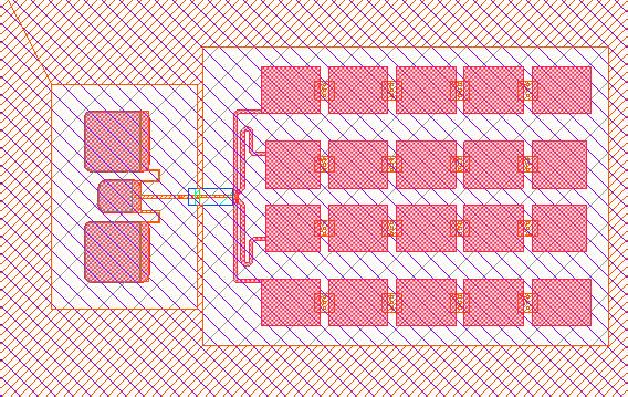
SIEVERT et al.: EC MODEL SEPARATING DISSIPATIVE AND RADIATIVE LOSSES 1291
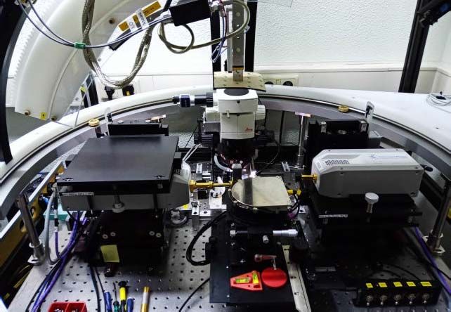
Fig. 16. Photograph of the antenna measurement setup from [39] with the
microscope over (a) wafer chuck and (b) within the reference measurement
of the horn antenna. (c) Closeup of the on-wafer probe with the mm-wave
absorbers. (d) Cross section sketch to indicate the effect of the absorber and
the metallic probe.
Fig. 15. Antenna assembly consisting of each two different antennas.
(a) Full EC model, including the feeding line. (b) Photograph from the on-chip
antenna. (c) Antenna modeled in the full-wave simulation software.
beamwidth, the antenna gain will be measured at a slightly
tilted angle (θ = 6◦ , marked with the blue line), where the
the EC model, but their influence is approximately included by effect of the absorber is assumed to be negligible. It should be
adding a TL section representing the electrical length between noted that the uncovered parts of the probe might still change
contacting probe tip and feeding line. the radiation pattern due to interference, as indicated with the
Due to a miscalculation during the design process, green lines (transmitted by the antenna and reflected from the
the desired quarter-wavelength transformers are electrically probe) in Fig. 16(d). Since the effect of the wafer probe is
too long, resulting in missing the desired input impedance an artifact of the measurement and, thus, not included in the
level. The intention of this feeding network, to distribute the far-field calculated by the EC model, the validation of the
power frequency dependent, is thus only sub-optimally ful- model will be carried out in two steps. First, the antenna
filled, which decreases the bandwidth covered by the antenna gain calculated by the full-wave FDTD simulation will be
assembly. Furthermore, a thin passivation SiN-layer between compared with the antenna gain predicted by the EC model,
the uppermost metal layers has been underestimated in its both without the effect of the wafer probe. Second, the antenna
effect. For the patch antennas utilized usually, this layer is neg- gain measured with the setup will be compared with the
ligible. Since the presented antenna includes coupling capac- gain calculated by the full-wave simulation, both including
itances utilizing this layer, it is extraordinarily sensitive to the uncovered-part of the wafer probe. In Fig. 17(a), the EC
the permittivity of this layer. As a consequence, the operation predicts both a steeper increasing gain toward the operation
frequency of each antenna pair will be decreased to 295 and frequency but also a lower gain compared with the full-wave
305 GHz. To account for this effect, the EC-extraction process simulation. The utilized EC model neglects both the coupling
has been carried out again, including the SiN-layer in the between the antennas and undesired radiation contributions
full-wave simulations and, thus, in the EC model. The results from the feeding network, e.g., from microstrip bends. These
presented from now on are based on the corrected EC model. neglected effects are identified to explain the difference to
For the on-chip antenna measurement, the spherical antenna the full-wave simulations, as the single antenna element has
measurement system presented in [39] was set up to measure been described by the EC with very good accuracy (see
the copolarization of the antenna. The measurement setup Section V). Here, only the gain, not the realized gain, is shown
with the microscope over the wafer chuck and the reference to exclude the impedance mismatch, as the EC uses only a
horn antenna is depicted in Fig. 16(a) and (b), respectively. simple TL to model the probing pads. Considering this simple
To reduce the effect of the metallic on-wafer probe on the modeling, the input impedance in Fig. 17(c) shows a good
measured radiation pattern, its frontside facing the antenna was agreement between the EC model and the measured input
covered with an mm-wave absorber [see Fig. 16(c)]. The effect impedance. Around the operation frequency of the antennas,
of the absorber and the metallic probe is sketched in Fig. 16(d). a more capacitive behavior resulting in an increased reflection
Due to the proximity of absorber and antenna, the radiated coefficient is calculated by the circuit simulation compared
far-field in the broadside direction (θ = 0◦ , marked with with the on-chip measurement. As explained earlier, the design
the red line) is attenuated, thus no reliable measure for error concerning the SiN-layer and the erroneous length of
the antenna’s gain. Since the antenna has a relatively large the quarter-wavelength transformers results in both detuned1292 IEEE TRANSACTIONS ON MICROWAVE THEORY AND TECHNIQUES, VOL. 69, NO. 2, FEBRUARY 2021
Fig. 18. Comparison of measured and simulated radiation pattern, including
the influence of the probe tip at (a) 295 and (b) 305 GHz. Only each half
cut-plane is shown, as the negative E-plane is obscured by the probe, and
the H-plane should be symmetric. The blue line highlights the tilted angle
explained in Fig. 16 (d) and used in Fig. 17(a) and (b).
In conclusion, the good agreement between the measured
and simulated gains over the operating bandwidth implies
two key outcomes. First, the consideration of the SiN layer
within the simulation is crucial for this antenna type and
needs to be included in the extracted EC models. Second,
from the good agreement of the realized gain for measurement
and simulation, one can conclude that directivity, impedance
Fig. 17. Antenna measurement and simulation comparing (a) gain without mismatch, and radiation efficiency calculated by the FDTD
the effect of the probe tip (w/o) for EC and full-wave solution, (b) realized
gain including the effect of the probe tip (w) comparing the full-wave solution simulation are correct. Furthermore, given that coupling effects
and the measurement, and (c) input impedance at the probe pads for EC and have been neglected, the gain calculated by the EC model
measurement. of the antenna assembly matches the simulation result well.
Finally, even the input impedance estimated by the EC is in
good agreement with the on-chip measurement. This implies
antennas and not well-matched input impedance. Furthermore, that the modeling of materials, conductor, and dielectric
Fig. 17(b) compares the realized gain of simulation and losses within the FDTD simulation and extracted EC are still
measurement, including the effect of the probe tip. Here, valid at mm-wave frequencies, even for complicated antenna
a very good agreement between simulation and measurement structures.
can be shown. The realized gain has been calculated based
on the gain of a reference horn antenna [see Fig. 16(b)], VII. C ONCLUSION
including the compensation for the losses of the wafer probe This article has presented an EC to model microstrip-based
and the additionally inserted waveguide sections [40]. Both antennas supplemented with series capacitances. The modeling
the measured and simulated realized gain peak at 295 GHz, of the utilized antenna parts is based on the extraction of
where the measured gain is even larger compared with the EC parameters from full-wave simulations while separating
simulated gain. In contrast to that, the simulated antenna with radiation and dissipation mechanisms. Each of the EC models
the probe tip predicts a drastically decreased gain at 305 GHz, describes a specific antenna part, and being cascaded, they
which can neither be seen at the measurement result nor at model the antenna assembly. The resulting EC model can
the gain of the antenna without probe tip [see Fig. 17(a)]. be used to calculate the antenna efficiency, input impedance,
Here, it appears that the modeling of the metallic on-wafer and broadside gain in excellent agreement with the full-wave
probe in the full-wave simulation is not ideal, resulting in simulation results. Furthermore, this EC model allows for
different interference effects in the simulation and the mea- initial analytical considerations based on a homogenized
surement. To prove this hypothesis, E- and H-planes have antenna model easing the design process by a presented
been measured and are shown in Fig. 18 for 295 and 305 GHz. design rule. Consequently, a computationally efficient calcu-
While the agreement between simulation and measurement lation of antenna parameters using only a circuit simulation
is acceptable for 295 GHz, strong deviations between both can be carried out in the order of seconds, which is an
results can be seen at 305 GHz. It should be emphasized that essential improvement compared with structural efficient, but
the antenna is influenced by the metallic probe tip and that still long-lasting FDTD simulations in the order of hours.
the differences observed are due to the modeling of the probe Based on this fast antenna characterization, an EC-based
tip in the full-wave simulation, which seems not sufficiently antenna optimization for maximized radiation efficiency with
detailed. the constraints of on-chip antennas is conceivably possible.SIEVERT et al.: EC MODEL SEPARATING DISSIPATIVE AND RADIATIVE LOSSES 1293
To verify the radiation efficiency calculated by the FDTD sim- [15] M. Uzunkol, O. D. Gurbuz, F. Golcuk, and G. M. Rebeiz, “A 0.32
ulation and prove that the modeling of conductor and dielectric THz SiGe 4×4 imaging array using high-efficiency on-chip anten-
nas,” IEEE J. Solid-State Circuits, vol. 48, no. 9, pp. 2056–2066,
losses has been carried out thoroughly, an mm-wave on-chip Sep. 2013.
antenna has been fabricated. Here, a very good agreement [16] D. L. Cuenca and J. Hesselbarth, “Self-aligned microstrip-fed spheri-
between the measured and simulated realized gains has been cal dielectric resonator antenna,” in Proc. 9th Europ. Conf. Antennas
Propag. (EuCAP), Lisbon, Portugal, Apr. 2015, pp. 1–5.
achieved after correcting two design mistakes. Furthermore, [17] P. Stärke, D. Fritsche, S. Schumann, C. Carta, and F. Ellinger, “High-
the EC model of the array assembly is in good agreement efficiency wideband 3-D on-chip antennas for subterahertz applications
with the full-wave simulation results, despite that antenna- demonstrated at 200 GHz,” IEEE Trans. THz Sci. Technol., vol. 7, no. 4,
pp. 415–423, Jul. 2017.
to-antenna coupling is not included in the EC model. Thus, it is [18] X.-D. Deng, Y. Li, C. Liu, W. Wu, and Y.-Z. Xiong, “340 GHz on-
claimed that both the FDTD simulation and the EC model are chip 3-D antenna with 10 dBi gain and 80% radiation efficiency,” IEEE
valid representations of real on-chip antennas. Based on the Trans. THz Sci. Technol., vol. 5, no. 4, pp. 619–627, Jul. 2015.
extraction method yielding the EC model, further efficiency [19] A. Dyck et al., “A transmitter system-in-package at 300 GHz with an off-
chip antenna and GaAs-based MMICs,” IEEE Trans. THz Sci. Technol.,
optimization, increased physical insight, and more advanced vol. 9, no. 3, pp. 335–344, May 2019.
antenna designs can be developed systematically. [20] A. Shamim, K. N. Salama, E. A. Soliman, and S. Sedky, “On-chip
antenna: Practical design and characterization considerations,” in Proc.
14th Int. Symp. Antenna Technol. Appl. Electromagn. Amer. Electro-
ACKNOWLEDGMENT magn. Conf., Ottawa, ON, Canada, Jul. 2010, pp. 1–4.
[21] C. A. Balanis, Antenna Theory: Analysis and Design, 3rd ed. Hoboken,
The authors are grateful to Infineon Technologies AG for NJ, USA: Wiley, 2005.
manufacturing and providing the test chip with the on-chip [22] L. Lewin, “Spurious radiation from microstrip,” Proc. Inst. Electr. Eng.,
antenna and Klaus Aufinger, Infineon Technologies, for his vol. 125, no. 7, pp. 633–642, Jul. 1978.
[23] J. James and A. Henderson, “High-frequency behaviour of microstrip
extensive and valuable consultation. open-circuit terminations,” IEE J. Microw. Opt. Acoust., vol. 3, no. 5,
pp. 205–218, Sep. 1979.
R EFERENCES [24] C. Caloz and T. Itoh, Electromagnetic Metamaterials: Transmission
Line Theory and Microwave Applications: The Engineering Approach.
[1] T. Jaeschke, C. Bredendiek, and N. Pohl, “A 240 GHz ultra-wideband Hoboken, NJ, USA: Wiley, 2006.
FMCW radar system with on-chip antennas for high resolution radar [25] J. Al-Eryani, H. Knapp, J. Kammerer, K. Aufinger, H. Li, and L. Maurer,
imaging,” in IEEE MTT-S Int. Microw. Symp. Dig., Jun. 2013, pp. 1–4. “Fully integrated single-chip 305–375-GHz transceiver with on-chip
[2] G. P. Kniffin and L. M. Zurk, “Model-based material parameter esti- antennas in SiGe BiCMOS,” IEEE Trans. THz Sci. Technol., vol. 8,
mation for terahertz reflection spectroscopy,” IEEE Trans. THz Sci. no. 3, pp. 329–339, May 2018.
Technol., vol. 2, no. 2, pp. 231–241, Mar. 2012. [26] P. Benedek and P. Silvester, “Equivalent capacitances for microstrip gaps
[3] K. K. Tokgoz et al., “A 120 Gb/s 16 QAM CMOS millimeter-wave and steps,” IEEE Trans. Microw. Theory Techn., vol. MTT-20, no. 11,
wireless transceiver,” in IEEE Int. Solid-State Circuits Conf. (ISSCC) pp. 729–733, Nov. 1972.
Dig. Tech. Papers, Feb. 2018, pp. 168–170. [27] M. Maeda, “An analysis of gap in microstrip transmission lines,”
[4] T. Hirano, K. Okada, J. Hirokawa, and M. Ando, “60 GHz on-chip patch IEEE Trans. Microw. Theory Techn., vol. MTT-20, no. 6, pp. 390–396,
antenna integrated in a 0.18-μm CMOS technology,” in Proc. Int. Symp. Jun. 1972.
Antennas Propag. (ISAP), Nagoya, Japan, Oct. 2012, pp. 62–65. [28] R. W. Jackson and D. M. Pozar, “Full-wave analysis of microstrip
[5] R. Han et al., “A 280-GHz Schottky diode detector in 130-nm digital open-end and gap discontinuities,” IEEE Trans. Microw. Theory Techn.,
CMOS,” IEEE J. Solid-State Circuits, vol. 46, no. 11, pp. 2602–2612, vol. MTT-33, no. 10, pp. 1036–1042, Oct. 1985.
Nov. 2011. [29] E. O. Hammerstad, “Equations for microstrip circuit design,” in Proc.
[6] Z. Chen, C.-C. Wang, H.-C. Yao, and P. Heydari, “A BiCMOS W-band 5th Eur. Microw. Conf., Hamburg, Germany, Oct. 1975, pp. 268–272.
2×2 focal-plane array with on-chip antenna,” IEEE J. Solid-State [30] H. A. Wheeler, “Transmission-line properties of parallel wide strips
Circuits, vol. 47, no. 10, pp. 2355–2371, Oct. 2012. by a conformal-mapping approximation,” IEEE Trans. Microw. Theory
[7] B. Sievert, D. Erni, and A. Rennings, “Resonant antenna periodically Techn., vol. MTT-12, no. 3, pp. 280–289, May 1964.
loaded with series capacitances for enhanced radiation efficiency,” [31] H. A. Wheeler, “Transmission-line properties of parallel strips separated
in Proc. 12th German Microw. Conf. (GeMiC), Stuttgart, Germany, by a dielectric sheet,” IEEE Trans. Microw. Theory Techn., vol. MTT-13,
Mar. 2019, pp. 20–23. no. 2, pp. 172–185, Mar. 1965.
[8] T. Zwick, D. Liu, and B. P. Gaucher, “Broadband planar superstrate [32] R. Owens, “Accurate analytical determination of quasi-static microstrip
antenna for integrated millimeterwave transceivers,” IEEE Trans. Anten- line parameters,” Radio Electr. Eng., vol. 46, no. 7, pp. 360–364,
nas Propag., vol. 54, no. 10, pp. 2790–2796, Oct. 2006. Jul. 1976.
[9] S. Beer, H. Gulan, C. Rusch, and T. Zwick, “Coplanar 122-GHz antenna
[33] D. M. Pozar, Microwave Engineering, 4th ed. Hoboken, NJ, USA: Wiley,
array with air cavity reflector for integration in plastic packages,” IEEE
2012.
Antennas Wireless Propag. Lett., vol. 11, pp. 160–163, Mar. 2012.
[34] H. Wheeler, “Formulas for the skin effect,” Proc. IRE, vol. 30, no. 9,
[10] B. Klein, R. Hahnel, and D. Plettemeier, “Dual-polarized integrated
pp. 412–424, Sep. 1942.
mmWave antenna for high-speed wireless communication,” in Proc.
IEEE-APS Topical Conf. Antennas Propag. Wireless Commun. (APWC), [35] D. E. Goldberg, Genetic Algorithms in Search, Optimization, and
Cartagena des Indias, Columbia, Sep. 2018, pp. 826–829. Machine Learning. Reading, MA, USA: Addison-Wesley, 1989.
[11] P. V. Testa, B. Klein, R. Hannel, C. Carta, D. Plettemeier, and F. Ellinger, [36] L. Lewin, “Radiation from discontinuities in strip-line,” Proc. IEE,
“Distributed power combiner and on-chip antennas for sub-THz multi- vol. 107, no. 12, pp. 163–170, Sep. 1960.
band UWB receivers,” in Proc. IEEE Int. RF Microw. Conf. (RFM), [37] H. Sobal, “Radiation conductance of open-circuit microstrip (correspon-
Penang, Malaysia, Dec. 2018, pp. 139–142. dence),” IEEE Trans. Microw. Theory Techn., vol. MTT-19, no. 11,
[12] D. L. Cuenca, J. Hesselbarth, and G. Alavi, “Chip-mounted dielectric pp. 885–887, Nov. 1971.
resonator antenna with alignment and testing features,” in Proc. 46th [38] R. E. Collin, Antennas and Radiowave Propagation (McGraw-Hill
Eur. Microw. Conf. (EuMC), London, U.K., Oct. 2016, pp. 723–726. Series in Electrical Engineering), 1st ed. New York, NY, USA:
[13] B. Sievert, J.-T. Svejda, D. Erni, and A. Rennings, “Mutually coupled McGraw-Hill, 1985.
dielectric resonators for on-chip antenna efficiency enhancement,” in [39] B. Sievert, J. T. Svejda, D. Erni, and A. Rennings, “Spherical
Proc. 2nd Int. Workshop Mobile THz Syst. (IWMTS), Bad Neuenahr, mm-Wave/THz antenna measurement system,” IEEE Access, vol. 8,
Germany, Jul. 2019, pp. 1–4. pp. 89680–89691, 2020.
[14] C.-H. Li and T.-Y. Chiu, “340-GHz low-cost and high-gain on-chip [40] T. Zwick, C. Baks, U. Pfeiffer, D. Liu, and B. Gaucher, “Probe based
higher order mode dielectric resonator antenna for THz applications,” MMW antenna measurement setup,” in Proc. IEEE Antennas Propag.
IEEE Trans. THz Sci. Technol., vol. 7, no. 3, pp. 284–294, May 2017. Soc. Symp., vol. 1, Jun. 2004, pp. 747–750.You can also read