IN3SBTE2 AS A PROGRAMMABLE NANOPHOTONICS MATERIAL PLATFORM FOR THE INFRARED
←
→
Page content transcription
If your browser does not render page correctly, please read the page content below
ARTICLE
                  https://doi.org/10.1038/s41467-021-21175-7                 OPEN

                  In3SbTe2 as a programmable nanophotonics
                  material platform for the infrared
                  Andreas Heßler 1 ✉, Sophia Wahl1, Till Leuteritz2, Antonios Antonopoulos1, Christina Stergianou1,
                  Carl-Friedrich Schön1, Lukas Naumann2, Niklas Eicker1, Martin Lewin1, Tobias W. W. Maß1, Matthias Wuttig                                                 1,

                  Stefan Linden 2 & Thomas Taubner 1 ✉
1234567890():,;

                  The high dielectric optical contrast between the amorphous and crystalline structural phases
                  of non-volatile phase-change materials (PCMs) provides a promising route towards tuneable
                  nanophotonic devices. Here, we employ the next-generation PCM In3SbTe2 (IST) whose
                  optical properties change from dielectric to metallic upon crystallization in the whole infrared
                  spectral range. This distinguishes IST as a switchable infrared plasmonic PCM and enables a
                  programmable nanophotonics material platform. We show how resonant metallic nanos-
                  tructures can be directly written, modified and erased on and below the meta-atom level in an
                  IST thin film by a pulsed switching laser, facilitating direct laser writing lithography without
                  need for cumbersome multi-step nanofabrication. With this technology, we demonstrate
                  large resonance shifts of nanoantennas of more than 4 µm, a tuneable mid-infrared absorber
                  with nearly 90% absorptance as well as screening and nanoscale “soldering” of metallic
                  nanoantennas. Our concepts can empower improved designs of programmable nanophotonic
                  devices for telecommunications, (bio)sensing and infrared optics, e.g. programmable infrared
                  detectors, emitters and reconfigurable holograms.

                  1 Institute of Physics (IA), RWTH Aachen University, Aachen, Germany. 2 Physikalisches Institut, University of Bonn, Bonn, Germany. ✉email: hessler@physik.

                  rwth-aachen.de; taubner@physik.rwth-aachen.de

                  NATURE COMMUNICATIONS | (2021)12:924 | https://doi.org/10.1038/s41467-021-21175-7 | www.nature.com/naturecommunications                                  1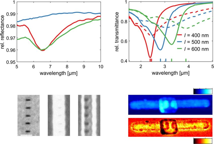
ARTICLE                                                                   NATURE COMMUNICATIONS | https://doi.org/10.1038/s41467-021-21175-7

M
           any recent technological advances in key areas like                Results
           telecommunication, lighting, health care, and solar                The phase-change material IST. PCMs are characterized by a
           energy harvesting have benefited from increasing con-               significant change of their optical properties upon crystallization,
trol over light. Confining light waves to ever-smaller length scales           which has been attributed to a change in bonding mechanism.
and thus overcoming Abbe’s diffraction limit enables ultra-                   Amorphous phase-change materials show the characteristic fea-
compact optical components1. Plasmonics achieves this goal by                 tures of covalently bonded materials (moderate optical dielectric
employing evanescent electromagnetic modes supported by                       constant ε∞, low electrical conductivity and an atomic arrange-
metallic nanostructures to concentrate light fields to deeply                  ment compatible with the 8-N rule20) like Phosphor and GaAs.
subwavelength regions2,3. Arranging plasmonic nanoantennas                    Covalently bonded materials share about two electrons between
(“meta-atoms”) in subwavelength assemblies in so-called meta-                 adjacent atoms and are therefore located in the red shaded region
surfaces allows for realizing ultrathin optical devices with exciting         of the bonding map44 in Fig. 1a (for a more detailed map see
functionalities like beam steering4, lensing5,6, and holography7,8.           Supplementary Fig. 1 and its description). Crystalline phase-
While these functionalities are originally fixed upon fabrication,             change materials such as GeTe, Sb2Te3 and Ge2Sb2Te5 (also called
they can be rendered active by multiple means including antenna               “incipient metals”20) on the contrary are characterized by an
geometry change by mechanical deformation9–11, charge carrier                 unconventional bonding mechanism coined metavalent
tuning by electric biasing12,13, and inducing an insulator-metal              bonding18,21,45 where about one electron is shared between
transition in VO2 by heating14–17. All of these tuning mechan-                adjacent atoms. Hence, ordinary phase-change materials like
isms are volatile, i.e., they only persist as long as an external             GeSbTe (GST) compounds are all located in the green shaded
stimulus is provided. In contrast, phase-change materials (PCMs)              region of the map (see e.g., the denoted area between GeTe and
offer non-volatile tuning. Because of the huge property contrast              Sb2Te3).
between their amorphous and crystalline phases resulting from a                  Remarkably now, crystalline IST has even less electrons shared
unique bonding mechanism18–21, they enable exciting tuneable                  between adjacent atoms40 and the electrons are significantly
functionalities like waveguiding22–24, chemical sensing25, light              delocalized, more akin to a metal (blue shaded region in the map).
detection26, and emission27, as well as lensing28. This makes them            The conductivity of IST at about 104 S/cm46 is correspondingly
prime candidates for non-volatile nanophotonic applications such              also about 10–1000 times larger than that of crystalline GST47.
as integrated optical memories, color displays, or active                     This metal-like conductivity in the crystalline state leads to a very
metasurfaces1,29. The resonance wavelength of antennas in                     different change of optical properties upon crystallization and the
metasurfaces is approximately proportional to the effective                   potential to exploit extraordinary functionalities, as will be shown
refractive index of the antennas’ dielectric environment and size.            below. While GST compounds can be classified as “incipient
So far, PCMs have been used in active metasurfaces29,30 to change             metals”, IST belongs to the material class of non-volatile “bad
the effective refractive index of the dielectric environment, lead-           metals”48, which form a bridge between the common PCMs and
ing to significant resonance shifts31,32. While PCMs have been                 metals. Here, we reveal the opportunities offered by this
successfully used previously to directly optically write dielectric           interesting material class and IST especially for programmable
antennas in thin PCM films33–35, the plasmonic properties of                   infrared nanophotonics. To emphasize this potential, we denote
typical PCMs have only recently been reported36,37. However,                  IST as a plasmonic PCM.
they are limited to the near-infrared spectral range by the                      The delocalization of electrons in the metavalent bond results
materials’ band gap, leaving the full infrared spectral range                 in an increased polarizability and thus larger permittivity of
unexplored, up to now. By employing the next-generation non-                  common PCMs in their crystalline phase than in their covalently
volatile plasmonic PCM In3SbTe2 (IST)38,39, we tap here into this             bound amorphous phase. This significant difference in permit-
unfulfilled potential for PCMs for infrared plasmonics. IST is a               tivity can also be observed in Fig. 1b, where the real part of the
semiconductor in the amorphous phase (aIST) but becomes                       permittivity ε‘ at 2.5 µm is plotted for several PCMs49 (see
metallic with negative permittivity in the whole-infrared range in            Supplementary Fig. 3 for more detailed permittivity plots). PCMs
the crystalline phase (cIST)40. Compared with other alternative               like GST compounds have a real permittivity ε‘ ≈ 10–20 in the
plasmonic materials41,42, IST’s optical properties can be optically           infrared spectral range in their amorphous structural phase, with
and locally switched. Thus, we propose a programmable nano-                   a negligible imaginary part. Upon crystallization, ε‘ increases by a
photonics material platform in the infrared based on it.                      factor of about two because of the change in bonding. These
   After comparing IST with common PCMs, we show how to                       PCMs are semiconductors in both phases50 and the real part of
write and erase plasmonic antenna arrays by optical switching                 their permittivity stays positive, ε‘ > 0, in this spectral region.
on the single meta-atom level. Additionally, we demonstrate                      However, for crystalline IST the case is different: Because the
flexible antenna reconfiguration on the sub-meta-atom level by                  electrons are delocalized similar to free electrons in a metal, IST
elongating, shortening and cutting individual rod antennas in                 changes from a semiconductor to a (bad) metal51 upon crystal-
half, causing significant resonance shifts. Next, we demonstrate               lization, exhibiting a change of the sign of the real part of the
optically tuneable, frequency-selective perfect absorbers based               permittivity ε‘ from positive to negative (blue point in Fig. 1b). In
on cIST. Finally, we demonstrate how IST can be used together                 Fig. 1c, the Drude-like permittivity of crystalline IST (blue) is
with conventional, prepatterned plasmonic metasurfaces to                     evident (zero-transition at about 900 nm, see Supplementary
either screen individual antennas from incident light or to                   Fig. 2) when compared to the permittivity of Ge3Sb2Te6 (GST-
“solder” them together. Our concepts could lead towards fast                  326).
and simple fabrication of plasmonic metasurfaces. Moreover,                      The marked difference of optical properties in the crystalline
they can empower programmable functionalities of plasmonic                    phase between IST and other PCMs gives access to different
devices for infrared optics, sensing and telecommunications.                  antenna resonance tuning mechanisms. Instead of changing the
One could devise, for example, real-time (bio)sensing, in-situ                refractive index Δn of an antenna’s dielectric surrounding, IST
pixel reprogramming of infrared detectors and displays, tune-                 can be used to directly change the antenna size by Δl or even
able localized optical heating, and delicate post-fabrication                 totally change the antenna shape itself. While the large refractive
metasurface adjustments to correct fabrication errors or min-                 index change has been shown to be a powerful tool, it is limited
utely adapt the functionality (e.g., realizing ultracompact                   by the naturally occurring refractive indices of PCMs (as
adaptive optics43).                                                           mentioned, they are usually about twice as large in the crystalline

2                 NATURE COMMUNICATIONS | (2021)12:924 | https://doi.org/10.1038/s41467-021-21175-7 | www.nature.com/naturecommunications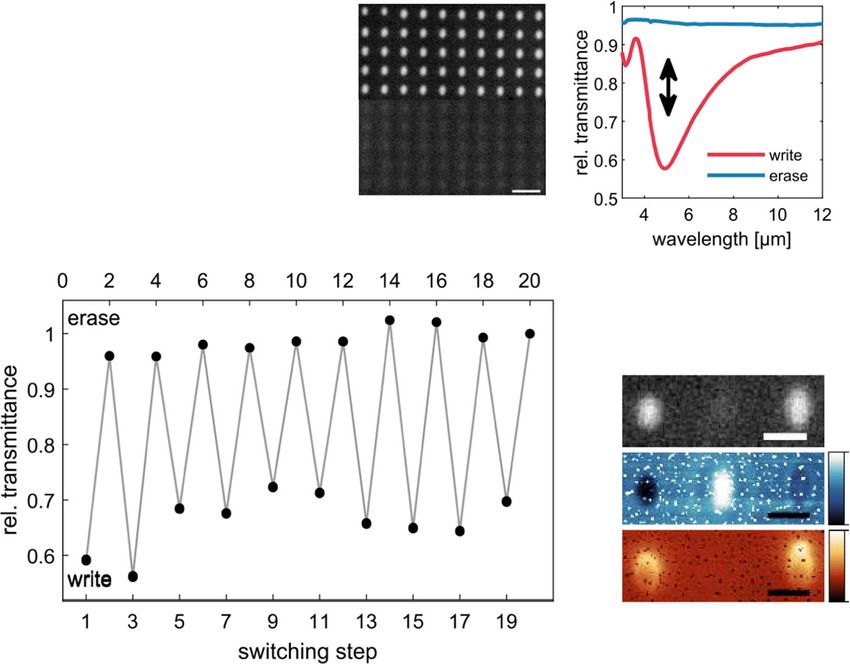
NATURE COMMUNICATIONS | https://doi.org/10.1038/s41467-021-21175-7                                                                        ARTICLE

                        a                                                        b

                        c                                                        d

                                                                                                        switchable
                                                                                                          metals

                                                                                                        alternative
                                                                                                          metals

                                                                                                                 common
                                                                                                                 metals

Fig. 1 Optical properties of In3SbTe2 (IST). a Zoomed-in map describing bonding in solids. It is spanned by the renormalized electron transfer between
adjacent atoms obtained after division by the formal oxidation state and the sharing of electrons between them. Common crystalline PCMs have
metavalent bonds (green shaded area) and metals have largely delocalized free electrons (blue shaded area). IST is part of the material class “bad metals”:
Its conductivity is significantly higher than that of other PCMs but smaller than that of metals. b The real part of the permittivity ε’ of IST (blue) in the
infrared at 2.5 µm changes sign upon phase change, unlike common PCMs like GeSbTe compounds49. c Real part of the electric permittivity in the infrared
of the crystalline and amorphous phases of GST-326 (green) and IST (blue), respectively, shown as a function of wavenumber. The data points from b are
marked. d Calculated Q factor of rod antennas in free space consisting of the indicated materials. The antennas are 1-µm long, 0.4-µm wide and arranged in
a square matrix with 2-µm period. IST as an antenna material is superior to VO2, TiN or AZO regarding the resonance quality.

phase than in the amorphous phase). In addition, the antenna is                  in the interband transition region and VO2 (see Supplementary
often not completely surrounded with PCM but, e.g., lies on a                    Fig. 5).
substrate, effectively lowering the influence of the PCM’s                           Active infrared metasurfaces based on PCMs can be switched
refractive index change. In contrast, there is almost no limit to                between multiple operation states via heating26,28, or short
the antenna reconfigurations that can be facilitated by IST: Even                 electrical53 and optical pulses33,34,54–57. The electrical and optical
subdiffraction switching becomes possible when combining                         switching of IST has been studied previously in the contexts of
crystallizing and amorphizing pulses. Thus, the accessible degrees               nanowires58 and data storage39, respectively. In the latter study, it
of freedom for designing infrared properties of antennas                         was demonstrated that IST can be optically switched without
significantly exceeds that available with other PCMs.                             phase separation on short time scales (about 50 ns). Optical
   As exploited by previous studies36,37, other PCMs, like GeSbTe                addressing has recently been used with GeSbTe alloys to fabricate
compounds, usually also have a small spectral window (mostly in                  thin-film dielectric metasurfaces33,34 and to program individual
the VIS-NIR) where ε‘ < 0 due to interband transitions at energies               meta-atoms in prepatterned PCM-incorporating metallic55 and
larger than the band gap energy. Because the charge carriers are                 dielectric metasurfaces56. Going one step further, it is now
not sufficiently delocalized, however, their permittivity does not                possible to directly write and erase metallic elements on and
follow the typical form of the Drude model and stays close to zero               below the meta-atom level in a metasurface containing a thin IST
there. As a measure for a material’s plasmonic performance in                    film by nanosecond laser pulses. Compared to conventional
nanoresonators52, in Fig. 1d we calculated the Q factors of rod                  lithography, no cumbersome additional steps like lift-off or
antennas in free space made from different materials (see                        etching are required and the whole metasurface can be erased and
Supplementary Fig. 4 for the optical properties). The Q factor                   rewritten fast and easily at any time. This vastly expands the
is defined as Q = ν/FWHM, where ν is the resonance frequency.                     possibilities of how PCMs can be employed in active
Common metals like Al and Ag have Q factors of about 6. It is                    metasurfaces.
noteworthy that Al has a slightly larger Q factor compared to Ag
due to its smaller skin depth in the infrared (7.7 nm for Al and
11 nm for Ag at a wavelength of 2.5 µm). The Q factor for IST is                 Optical writing and erasing of plasmonic nanoantennas. As a
about 4, which is significantly larger than that of VO2 and still                 platform for the following applications, we investigated how to
slightly larger than that of TiN and AZO (alternative metals41).                 write and erase plasmonic nanostructures on the meta-atom level
Not only for localized but also for propagating surface plasmon                  in a thin film of 50-nm thick aIST on a CaF2 substrate (see Fig. 2).
polaritons, IST has a superior figure of merit compared to GST                    To prevent oxidization and ablation, the IST layer is capped with

NATURE COMMUNICATIONS | (2021)12:924 | https://doi.org/10.1038/s41467-021-21175-7 | www.nature.com/naturecommunications                                   3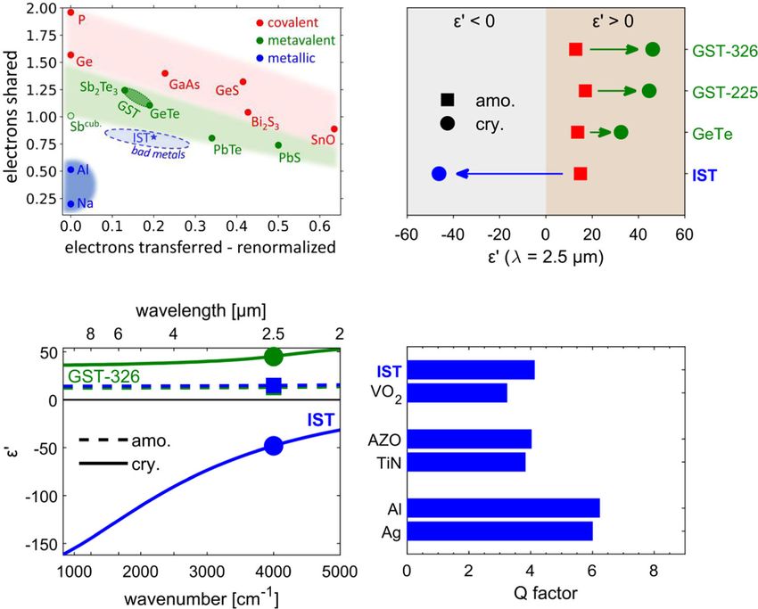
ARTICLE                                                                    NATURE COMMUNICATIONS | https://doi.org/10.1038/s41467-021-21175-7

                     a                                        b                              c
                                           ZnS:SiO2

                                                               write
                           70 nm
                                         IST
                      50 nm

                                                               erase
                                    CaF2

                     d                                                                       e
                                                                                                  write      erase rewrite

                                                                                                      cIST      aIST

                                                                                                                            h [nm]
                                                                                                                               7

                                                                                                                              0
                                                                                                                              1.8

                                                                                                                              0.6
                                                                                                                        s3/s3(aIST)

Fig. 2 Write and erase. a Sketch of the sample layer stack. b Light micrograph (scale bar 3 µm) of a cIST nanoantenna array written (top) and erased
(bottom) by optical switching. c FTIR transmittance measurements of the written and erased arrays from b. d Relative transmittance at 4.66 µm
(resonance minimum) for 20 switching steps. e Sketch, light microscope, AFM (height h) and s-SNOM (λ = 10.57 µm, see Methods) images of written,
erased and rewritten nanoantennas (scale bar is 1 µm).

a 70-nm thick layer of (ZnS)80:(SiO2)20 (see Fig. 2a). A light                 with a resolution that is well below the diffraction limit61. The
micrograph of an optically written cIST nanoantenna array is                   measured near-field optical amplitude signal s3 at a wavelength of
shown in Fig. 2b. A pulsed laser with a wavelength of 660 nm was               λ = 10.57 µm, referenced to the amplitude signal s3(aIST) of the
used for switching (see Methods). The bottom half of the array is              aIST, is shown in the bottom row of Fig. 2e. Again, only the
replaced with the image of the erased array, where the cIST of                 written and rewritten antennas, i.e., the cIST areas, are visible as
each antenna was reamorphized. As shown, only a faint shadow                   bright features. The erased antenna shows the same optical
of the antennas is left after erasing. The measured transmittance              contrast as the surrounding aIST film, confirming the successful
spectra of the written and erased arrays are shown in Fig. 2c. A               reamorphization.
clear resonance dip at λ = 4.66 µm is visible in the written state
(red), whereas the resonance is completely gone in the erased                  Optical antenna resonance control. After establishing the viable
state and almost unity transmittance is obtained (blue). To                    writing and erasing of metallic nanostructures in an IST thin film
demonstrate the performance over several switching cycles, the                 on the meta-atom level, we performed first proof-of-principle
transmittance at λ = 4.66 µm is plotted for the first 20 switching              experiments (see Fig. 3) to demonstrate the optical modification
steps in Fig. 2d. It consistently switches between about 0.65 in the           of infrared plasmonic antennas on the sub-meta-atom level.
written state (bottom axis) and about 1 in the erased state (top               This effectively lays the foundation for sub-pixel reconfiguration
axis). Finally, the written, erased and rewritten cIST nanoanten-              and pixel-by-pixel programming in plasmonic metasurfaces
nas are characterized by several microscopy methods (see Fig. 2e):             (1 pixel = 1 meta-atom).
light microscopy (LM), atomic force microscopy (AFM), and                         We employed the same layer stack as in Fig. 2a. Rod antennas
scattering-type near-field optical microscopy (s-SNOM, see                      were arranged in a 20 × 20 µm2 antenna array. After the initial
Methods). The top row contains a sketch of the three switching                 writing, the antenna lengths were subsequently changed by
states. Below that in the LM image, the written and rewritten cIST             switching the IST at the antenna tips. Figure 3a depicts the
antennas are distinguishable as bright areas, whereas the erased               measured infrared transmittance spectra of the corresponding
antenna is not visible and appears as dark as the rest of the aIST             antenna arrays (see light microscope images on the right). In each
film. The cIST areas appear bright because the real part of its                 spectrum, a minimum at the resonance wavelength (electric
permittivity ε‘ < 0 in the visible spectral range (because of inter-           dipole resonance) can be observed as well as smaller features at
band transitions), which results in high reflectance in the light               shorter wavelengths originating from the antenna grating orders.
microscope. In contrast, aIST has ε‘ > 0 in the visible spectral               The first antenna resonance lies at 5.7 µm (red). By crystallizing
range and thus reflects much less light. In the AFM topography                  the IST at the antenna tips (see dark gray, dotted ellipse in the top
image, however, all three cases can be discerned. The written and              sketch in Fig. 3a), the antennas are elongated and the resonance
rewritten cIST antennas are visible as depressions in the aIST film             then gradually redshifts up to a wavelength of 7.9 µm. Next, the
(decreased density of crystalline PCMs59), while the erased                    antennas were shortened by reamorphizing the IST at the
antenna shows a slight elevation in topography (microbump                      antenna tips (see white, dotted ellipse in the bottom sketch in
formation60). With s-SNOM, it is possible to measure the local                 Fig. 3a). This led to a gradual blueshift from 7.9 µm down to
infrared optical properties of the submicrometer crystalline areas             4.4 µm, totalling a complete tuning range of Δλ = 3.5 µm.

4                  NATURE COMMUNICATIONS | (2021)12:924 | https://doi.org/10.1038/s41467-021-21175-7 | www.nature.com/naturecommunications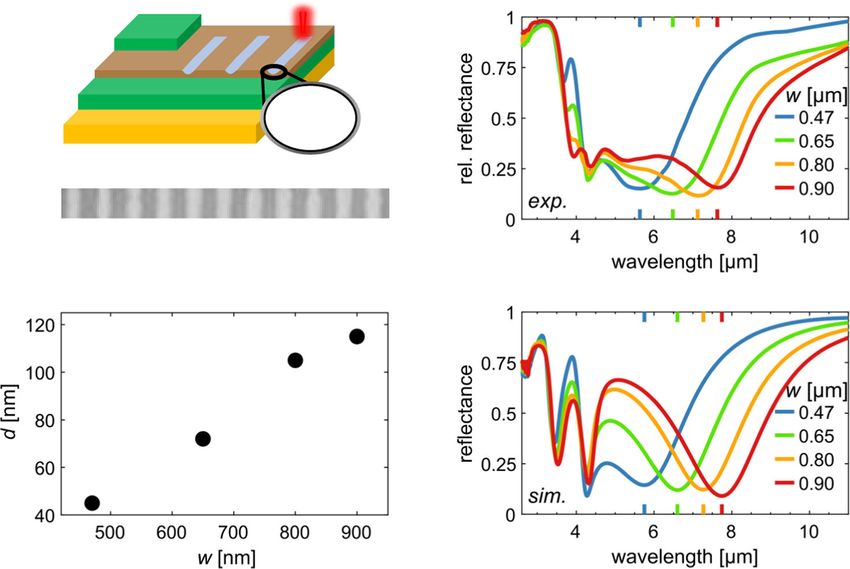
NATURE COMMUNICATIONS | https://doi.org/10.1038/s41467-021-21175-7                                                                       ARTICLE

                a                                                  b                                      c

                                                                                                          d

Fig. 3 Optical antenna resonance control. a Measured transmittance spectra of nanorod antenna arrays of different length (shifted on y-axis for clarity).
Light micrographs (transmittance mode) are shown on the right. The length was successively increased/decreased via crystallization/reamorphization at
one antenna end (see sketches). b Measured transmittance spectra of nanorod antenna arrays of different length l and adjusted period (shifted on y-axis
for clarity). Light microscope images of the antennas are depicted on the right. c Plot of the antenna length l against the measured resonance wavelength.
Blue data points are for antennas on a CaF2 substrate, orange data points for antennas on a Si substrate. The red lines are linear fits to the two data sets
and show good agreement with the data. d Measured transmittance spectra of long nanoantenna arrays (red) which were then optically cut in half (see
sketch) by reamorphization (blue). Corresponding light micrographs are depicted on the right. All scale bars are 2 µm.

   Remarkably, the antennas can be made even shorter via                         doped semiconductors64) or on phase-transition materials like
reamorphization than the initial cIST antennas. This results in a                VO216, where Δλ ≈ 1–2 µm.
significantly shorter resonance wavelength: 4.4 µm instead of                        The resonance wavelength (electric dipole) of classic metallic
5.7 µm. By overlapping slightly shifted (diffraction-limited)                    nanorod antennas follows the relation λres = neff2l + δ, where neff
crystallizing and reamorphizing laser pulses, it becomes possible                is the effective refractive index of the antenna’s dielectric
to achieve optically switched structures on a scale below the                    surrounding and δ is a constant offset parameter65. This linear
diffraction limit of the VIS switching laser.                                    relation is confirmed in Fig. 3c, where the antenna length is
   The longest antennas in Fig. 3a (green framed light micro-                    plotted against the resonance wavelength. The fit (red line) to the
graph) are already almost touching and cannot be elongated                       blue data points reveals the relation λres = 1.7·2l + 2.1 µm. Thus,
further. Longer antennas require a larger array period. Moreover,                the cIST antennas can be indeed described as plasmonic nanorod
the amplitude for the shortest antennas is dramatically reduced                  antennas. For substrates with a larger refractive index (e.g., about
due to their reduced area-density and cross-section. With our                    3.4 for Si instead of 1.4 for CaF2), the effective refractive index neff
proposed material platform based on IST, it is now possible to                   of the antennas’ dielectric surrounding, and thus their resonance
completely rearrange the antennas in the array in addition to                    wavelength, is increased. Accordingly, by adjusting the substrate
changing the antenna lengths (see Supplementary Movie 1).                        material, one can change the antenna lengths required for a
Figure 3b displays measured transmittance spectra and light                      certain spectral resonance position66 and optimize the resonance
micrographs of corresponding IST antenna arrays (see Methods),                   quality in that wavelength range (see Supplementary Fig. 7). As
demonstrating a tuning range of Δλ = 4.3 µm, which is more than                  can be seen from the orange data points in Fig. 3c, the resonance
20% larger than the tuning range achieved for the static array                   wavelengths of cIST antennas on Silicon are about 2–3 µm larger
periods in Fig. 3a. The experimental data are in good agreement                  than on CaF2 for the same antenna lengths and still follow a
with numerical simulations of infinite cIST antenna arrays of the                 linear trend over the antenna length. The lower slope of the linear
same dimensions (see Supplementary Fig. 6).                                      fit is due to Silicon’s larger refractive index. Moreover, the dipole
   The large total shift yields a large tuning figure of merit                    antenna characteristics of the cIST antennas could be confirmed
TFOM = Δλ/FWHM ≈ 1.9. Here, the FWHM = 2.3 µm of the                             with numerical field simulations of the electric, magnetic and
smallest antennas was considered in accordance with                              current density fields. Compared to gold antennas of the same
literature31,62. This is an exceptionally large TFOM value when                  dimensions, the field distributions are strikingly similar (see
compared with common GeSbTe compounds, which facilitate                          Supplementary Fig. 8).
resonance shifts of Δλ ≈ 1 µm and TFOM ≲ 1.232. The resonance                       Modifying cIST nanoantennas is not limited to adding or
tuning with IST of Δλ = 4.3 µm also surpasses other tuning                       removing cIST at the antenna ends. In Fig. 3d, it is demonstrated
concepts based on charge carrier density tuning (graphene63,                     that one can also directly access and modify the interior of

NATURE COMMUNICATIONS | (2021)12:924 | https://doi.org/10.1038/s41467-021-21175-7 | www.nature.com/naturecommunications                                  5
ARTICLE NATURE COMMUNICATIONS | https://doi.org/10.1038/s41467-021-21175-7
individual antennas (meta-atoms). As depicted in the sketch transmittance and the difference of the reflectance R to unity
(white dotted ellipse), the long nanorod antennas (red frame) equals the absorptance A = 1 − R. Moreover, absorption and
were “cut through” in the middle by a reamorphizing pulse, emission are linked by Kirchhoff’s law of thermal radiation. Thus,
resulting in two smaller rod antennas for each previous long good infrared absorbers are also good thermal emitters67. In our
antenna (blue frame). The measured transmittance spectra also experiment, we set the period to p = 2 µm and varied w between
reflect this with a blueshift of the resonance by 2.7 µm from 470 and 900 nm by adjusting the switching laser pulse duration.
8.2 µm to 5.5 µm. This is only exemplary for the freedom given The incident infrared light was polarized perpendicularly to the
for design and modification of nanostructures in our introduced bars. In the measured reflectance spectra (Fig. 4c), there is a
platform. One can switch the IST differently in each individual reflectance minimum at wavelengths larger than 5 µm (magnetic
meta-atom and for instance write a metasurface where the resonance) and 2 significant minima at wavelengths smaller than
antenna lengths increase along the array (see Supplementary 5 µm (thin-film resonances). The magnetic resonance is created
Fig. 9a). Going beyond the modification of simple rod antennas, by the oscillating charges in the cIST at the top and their mirror
one can also write freeform shapes (see Supplementary Fig. 9b), image in the Au at the bottom. When increasing the bar width w
as well as more complex resonator structures like split ring from 470 to 900 nm, one can now continuously spectrally tune
resonators by combining writing and erasing laser pulses (see the reflectance minimum associated with the magnetic resonance
Supplementary Fig. 10). between about 5 and 8 µm. The minimum reflectance is always
The creation of more complex structures also allows to access smaller than 15% and for w = 0.8 µm (green), it almost reaches
different resonance modes and to change between them: As down to 10%. This corresponds to a maximum absorptance of
shown, one can switch from a single electrical dipole to either two A ≈ 90 % and the tuning enables an absorptance modulation of
coupled electrical dipoles (cut nanorod) or to a magnetic dipole up to 65%.
(split ring resonator). Higher-order modes like quadrupole In Fig. 4c, the crystallization depth d is plotted against the bar
resonances could also become attainable by reshaping or coupling width w. It is determined by a comparison of minimum reflectance
of individual resonators. between simulations and measurements. The simulated spectra
(Fig. 4d) only fit well to the measured spectra if a vertical extent of
the cIST bars is assumed that is smaller than the total aIST film
Optical writing of frequency-selective infrared absorbers. In thickness (inset in Fig. 4a). The existence and importance of this
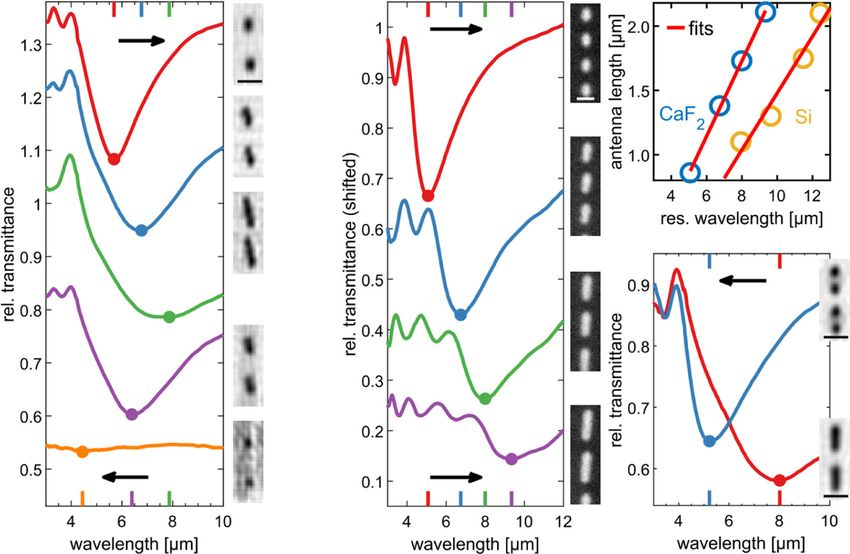
another proof-of-principle experiment for optically written plas- crystallization depth d for resonance tuning of GST-covered
monic IST metasurfaces, we fabricated a frequency-selective IR nanoantennas by optical switching has been demonstrated just
absorber (see Fig. 4). First, a 100-nm thick Au mirror is evapo- recently55,68. Due to different thermal properties of the layers above
rated onto a Si substrate. On top of that, 230 nm (ZnS)80:(SiO2)20, and below the aIST layer, a temperature gradient arises from top to
115 nm aIST, and 70 nm (ZnS)80:(SiO2)20 are deposited (Fig. 4a). bottom. Because the temperature is highest at the top (air is a bad
According to the previously discussed concepts of optical writing, thermal conductor), crystallization starts there and then proceeds
metallic cIST grating bars of variable width w and period p can be downwards. Experimentally, the different crystallization depths are
directly written into the unstructured layer stack (cf. Fig. 4b). realized by using increasing laser pulse durations for increasing cIST
The metallic bars and the Au bottom mirror form a resonant bar widths w (cf. Methods). The optical heating for longer times
infrared absorber system. Because of the Au mirror, there is 0 then allows for crystallization deeper into the aIST layer, resulting in
a laser b
d
Au aIST cIST ZnS:SiO2
w p = 2 µm
c d
Fig. 4 Optical writing of frequency-selective IR absorber. a Top: Sketch of the absorber layer stack and grating pattern structure. cIST bars of variable
width w and period p can be written into the surface with the pulsed laser. The inset sketches the crystallization depth d. Bottom: Light microscope image
excerpt of a cIST absorber, denoting the fixed period p = 2 µm and the bar width w. b Measured reflectance spectra of the IR absorbers with p = 2 µm
configured to absorb at different spectral ranges by changing the bar width w from 0.47 to 0.9 µm. The magnetic resonance positions are marked with
colored ticks. c Crystallization depth d of the simulated cIST bars vs. their width w. d Simulated reflectance spectra corresponding to b.
6 NATURE COMMUNICATIONS | (2021)12:924 | https://doi.org/10.1038/s41467-021-21175-7 | www.nature.com/naturecommunicationsNATURE COMMUNICATIONS | https://doi.org/10.1038/s41467-021-21175-7 ARTICLE
larger crystallization depths. For the given absorber structure, the resonance shift would originally be even larger, but the Au
crystallization depth is an important parameter because it not only antenna lengths decreased after annealing in the oven (see
defines the total crystallized volume but also the distance between Supplementary Fig. 13a). The kink in the spectra at smaller
the plasmonic structures and the metallic back-mirror, which is wavelengths results from grating resonances and thus stays at the
directly related to their electromagnetic coupling and the resulting same wavelength after switching the IST because the array
magnetic dipole moment. Only by optimizing the crystallization periodicity is conserved even though the antenna lengths slightly
depth, the absorptance can be maximized to close to 100% for a decrease. The resonance shift will generally increase even more
given layer stack (see Supplementary Fig. 11). for longer antennas and larger gaps (cf. Supplementary Fig. 13b).
Our frequency-selective IR absorber design has great potential The topography and near-field optical contrast (measured with s-
for thermal imaging applications (see Supplementary Fig. 12) and SNOM at a wavelength of λ = 10.57 µm) of a dimer with 600 nm
leads the way towards optical programming of light absorbers26 long antennas and a cIST patch are depicted in Fig. 5f. In both
for infrared color, both for detection and emission. This might for images, it is visible that the cIST patch in the dimer gap overlaps
example be employed for programmable simultaneous thermal with both antennas. Notably, the near-field contrast of the cIST
infrared invisibility and holographic illusion69. patch and the Au antennas is the same in the bottom image,
which signifies similar optical properties. This underlines again
the metallic infrared optical properties of crystalline IST.
Nanoscale screening and soldering. So far, we have used Multiple potential nanoantenna geometries can now be
unpatterend IST thin-films to directly optically write tuneable encoded on a single metasurface with strategically positioned
plasmonic antennas and active metasurfaces. In a different IST patches and then switched between by nanoscale soldering.
approach, one can also use IST to adjust prepatterned metallic On the one hand, this allows for minor adjustments, which is, e.g.,
antennas. Then, IST can either work like a nanoscale screen on important for compensating tight fabrication tolerances and for
the meta-atom level or like a “solder” for metallic nanostructures adaptive optics43. On the other hand, one can also realize major
on the sub-meta-atom level. A similar concept, though designed reconfigurations like a total change of functionality, e.g., between
for large-area tuning, has very recently also been demonstrated beam focusing and beam steering. Please note that the switching
with the volatile phase-transition material VO270. of prepatterned IST structures is not limited to optical laser pulses
Generally, each individual nanoantenna in an IST-coated but can also be achieved via electrical voltage pulses58.
metasurface can be permanently switched off (antennas not
excited) and on (antennas excited) by optically switching the IST
above the antennas. In the crystalline state, the cIST area acts like Discussion
a mirror, which screens the antenna from the incident light and We introduced the next-generation, switchable, infrared plas-
thus prevents antenna excitation. This is demonstrated here for monic phase-change material In3SbTe2 (IST) as a material plat-
the case of an IST-coated Al slit antenna array on a Si substrate form for programmable plasmonics and nanophotonics in the
(see Fig. 5a). In Fig. 5b, measured reflectance spectra are plotted infrared. On the meta-atom level, we demonstrated direct writing
for three different switching states: the default on-state (red), the and erasing of metallic crystalline IST (cIST) nanoantennas into a
off-state with cIST above the slits (blue) and the restored on-state dielectric amorphous IST (aIST) thin film for 20 switching steps
with reamorphized IST above the slits (green). In the two on- and characterized them by diffraction-limited far-field as well as
states, there is a distinct reflectance minimum (slit resonance), super-resolution near-field measurement techniques. On the sub-
whereas it is gone in the off-state. In Fig. 5c, the corresponding meta-atom level, we demonstrate flexible antenna reconfiguration
light micrographs are displayed. Please note that the resolution of by elongating, shortening and cutting individual rod antennas in
these images is limited by diffraction and that the shape of the half, tuning the infrared plasmonic antenna resonances by more
slits does not change because of the switching. than 4 µm. Subsequently, a tuneable broad-band infrared absor-
Until now, the switching of IST was performed optically and ber with absorptance of nearly 90%, a mid-infrared spectral
was therefore limited by diffraction of the red light of the tuning range of about 3 µm and an absorption amplitude tuning
switching laser. In case the IST needs to be switched at even range of about 65% was shown. Nanoscale screening of pre-
smaller scales, it can be prepatterned with nanofabrication patterned antennas with a thin IST film results in an on/off
methods like electron beam lithography. In this way, ultrasmall functionality, while strategically positioned IST patches allow for
IST switches can be strategically arranged on a metasurface and nanoscale “soldering” of individual meta-atoms.
selectively toggled between dielectric and metallic optical proper- These concepts are fundamentally impossible to achieve with
ties at the sub-meta-atom level. As an application, we show how common dielectric PCMs (e.g., GeSbTe alloys). In addition to a
the two rods in a gold dimer antenna can be conductively large resonance tuning, IST enables the creation of complex
connected by a small patch of IST positioned in the dimer gap plasmonic structures with different resonance modes. The optical
(Fig. 5d). Thus, two neighbouring, separated nanoantennas can switching can be easily scaled up and parallelized (e.g., by laser
be turned into a single long nanoantenna. The results of such interference lithography) towards large-area fabrication with high
switching for a dimer antenna array with IST-bridged 100 nm throughput. Our work thus lays the foundation for a program-
dimer gaps are shown in the transmittance measurements in mable nanophotonics material platform for the infrared. It also
Fig. 5e. There, 50-nm thick IST and 10-nm thick ZnS:SiO2- holds great potential for application in integrated photonics,
capping are deposited exclusively at the 100 nm dimer gap of where, reconfigurable plasmonic components for, e.g., routing,
150-nm wide, 30-nm thick Au antennas of different lengths l and waveguiding and filtering are now made possible by optically or
period p = 2.4 l. The aIST was then crystallized by heating on a electrically switched IST elements. The extension of our
hotplate (see Methods). In the plotted transmittance spectra, the frequency-selective near-perfect IR absorber could lead towards
spectral redshift of the transmittance minimum (resonance) from real-time biosensing or the in-situ reprogramming of infrared
aIST (solid lines) to cIST (dashed lines) patches is observable for detectors and displays working in absorption or emission mode.
each length l. This resonance shift resulting from the conductive A thin IST layer on top of negative permittivity materials that
connection between the dimer antennas becomes larger with host surface waves such as polar crystals (phonon polariton) or
increasing l. For l = 600 nm, it is about 600 nm large, which doped semiconductors (plasmon polariton) could enable the
corresponds to a tuning figure of merit of about 0.7. Here, the writing of nanophotonic elements for polaritons like deeply
NATURE COMMUNICATIONS | (2021)12:924 | https://doi.org/10.1038/s41467-021-21175-7 | www.nature.com/naturecommunications 7ARTICLE NATURE COMMUNICATIONS | https://doi.org/10.1038/s41467-021-21175-7
a d
p
cap
70 nm cap
50 nm IST IST
40 nm Al Au
800 nm Si glass
l
b e
c f h [nm]
on off on
0 150
AFM
SNOM
0.3 1.4
s2/s2(Au)
Fig. 5 Nanoscale screening and soldering of nanoantennas with In3SbTe2. a Cross-section sketch of the full layer stack of an IST-covered Al slit antenna.
The cIST (light blue) does not reach down completely through the aIST (brown) to the Al (silver). b FTIR reflectance spectra of slit arrays for the default on-
state (red), the off-state (blue) and the restored on-state (green). c Light microscope image excerpts of the arrays measured in b (scale bar: 2 µm). d Cross-
section sketch of the array unit cell with a gold dimer antenna on glass whose gap is bridged with an IST patch. e Measured transmittance spectra of the dimer
antenna arrays with different antenna lengths l (400 nm, 500 nm, 600 nm) and period p = 2.4l for aIST (solid) and cIST (dashed). With cIST the dimers are
soldered together and the resonance redshifts (see colored ticks at the bottom). f AFM (top) and s-SNOM (bottom) images of a gold dimer soldered together
with cIST: In the s-SNOM image, the cIST patch has the same optical contrast as the Au antennas, verifying its metallic infrared optical properties.
subwavelength resonators or waveguides17,34,71,72. Composing Switching of IST. The localized phase change of the IST thin-films was realized
dielectric metasurfaces56,57,73–75 out of amorphous IST could with an in-house-built laser setup55. A pulsed laser beam (wavelength λ = 660 nm)
is focused through a 10-fold objective with a numerical aperture of 0.5 on the
enable the switching from narrow Mie resonances to broad sample surface. The sample is placed on a Thorlabs NanoMax-TS (Max311/M)
plasmonic resonances. Finally, the non-volatile switching of IST stage, which is movable in x-, y-, and z-direction and connected to a Thorlabs
could be combined with the dynamic, volatile tuning methods closed-loop piezo controller (BPC303). A custom program allows for the auto-
offered by materials like VO2, leading to interesting functional- mated positioning of pulsed laser shots on the sample surface within 5 nm accu-
ities like multilevel, intelligent switches76,77. racy. By using long (~500 ns) and low-powered (~10 mW) laser pulses, an IST thin
film can be locally crystallized by heating it above the glass transition temperature.
The crystallized area has an elliptical shape, whose size can be tuned by changing
the laser parameters (pulse power, pulse duration and number of pulses)55, see e.g.,
Methods Supplementary Fig. 7b. By using short (~20 ns) and high-powered pulses
Sample fabrication. In3SbTe2 (IST) was deposited on the substrates by direct (~300 mW), the crystalline PCM can be melted locally by heating it above the
current magnetron sputtering, while (ZnS)80:(SiO2)20 was deposited with radio melting temperature, after which a rapid cooling (>109 K/s) yields amorphization.
frequency magnetron sputtering. A LS 320 von Ardenne systems (base pressure The laser pulse parameters [power, duration, number of pulses] for Fig. 2 are
2 ∙ 10−6 mbar, 20 s.c.c.m. Ar flow, deposition rates 1 Å/s for IST and 0.3 Å/s for [7.2 mW, 500 ns, 1000] for crystallization and [281 mW, 10 ns, 1] for ream-
ZnS:SiO2) was operated in constant power mode (24 W for IST and 59 W for orphization. For Fig. 3a, the laser pulse parameters are [8.2 mW, 500 ns, 1000] for
ZnS:SiO2) using stoichiometric targets of 99.99% purity. The Al slit antennas crystallization and [205 mW, 10 ns, 1] and the array periods are [px, py] = [2.2 µm,
were fabricated by first thermally evaporating Aluminum (2 Å/s, 2 × 10⁻⁵ mbar 3.5 µm]. For Fig. 3b, the laser pulse parameters are [7.2 mW, 500 ns, 1000] and
base pressure) onto a Si substrate and then patterning the Al thin film with the antenna array dimensions [l, px, py] in µm are measured by light microscopy
focused ion beam milling with a Helios NanoLab DualBeam 650 by FEI com- and given as [0.9, 2.1, 1.8], [1.4, 2.9, 2.2], [1.7, 3.8, 2.6] and [2.1, 4.7, 3.0]. For
pany (30 kV acceleration voltage, 83 pA beam current, 3 µs dwell time). The gold Fig. 3c, the laser pulse parameters are [8.2 mW, 500 ns, 1000] for crystallization and
dimer antennas with IST in their gaps were fabricated by two-step electron beam [182.3 mW, 10 ns, 1] for reamorphization the array periods are [px, py] = [2.2 µm,
lithography with PMMA as resist and Electra92 as conductive polymer. In the 3.5 µm]. In Fig. 4, the employed laser pulse power is 0.4 mW, the number of pulses
first step, gold was evaporated onto the patterned resist. After a lift-off process, is 500 and the pulse durations for the respective bar widths are: 250 ns for w =
the gold dimer antennas are left on the glass substrate. In the second step, the 0.47 µm, 310 ns for w = 0.65 µm, 340 ns for w = 0.8 µm, and 370 ns for w = 0.9 µm.
resist was only patterned in the gaps of the dimers. Onto this patterned resist, The switching parameters for screening the slits in Fig. 5a, b are [53.5 mW, 1000 ns,
50 nm IST and 10 nm (ZnS)80:(SiO2)20 were sputtered (see above). After another 150] for crystallization and [394.5 mW, 10 ns, 1] for reamorphization. For crys-
lift-off process, the finished gold dimers with IST in their gaps are left on the tallizing the IST patches in the dimer gaps in Fig. 5c–e, the sample was heated
glass substrate. uniformly on in an oven at 250 °C for 30 min.
8 NATURE COMMUNICATIONS | (2021)12:924 | https://doi.org/10.1038/s41467-021-21175-7 | www.nature.com/naturecommunicationsNATURE COMMUNICATIONS | https://doi.org/10.1038/s41467-021-21175-7 ARTICLE
FTIR spectroscopy. The Fourier transform infrared (FTIR) spectroscopy data 16. Kats, M. A. et al. Thermal tuning of mid-infrared plasmonic antenna arrays
were collected using a Bruker Vertex 70 interferometer coupled to a Bruker using a phase change material. Opt. Express 38, 368 (2013).
Hyperion 2000 microscope. The FTIR measurement parameters for the data from 17. Folland, T. G. et al. Reconfigurable infrared hyperbolic metasurfaces using
the Figures is as follows: 1000 scans with 16 cm−1 spectral resolution for Figs. 2, 3, phase change materials. Nat. Commun. 9, 4371 (2018).
and 5; 2000 scans with 32 cm−1 spectral resolution for Fig. 4. For the measure- 18. Wuttig, M. & Yamada, N. Phase-change materials for rewriteable data storage.
ments from Figs. 3 and 4, ×15 Cassegrain objectives were used, for all the other Nat. Mater. 6, 824–832 (2007).
measurements ×36 objectives. The area around the antenna arrays was excluded 19. Raty, J.-Y. et al. A quantum-mechanical map for bonding and properties in
from the measurement with knife edge apertures and the polarization was along solids. Adv. Mater. 31, 1806280 (2018).
the long antenna axes in Figs. 2, 3, and 5e, and perpendicular to the grating bars 20. Wuttig, M., Deringer, V. L., Gonze, X., Bichara, C. & Raty, J.-Y. Incipient
and slits in Figs. 4 and 5b, respectively. For all measurements the free area on the metals: functional materials with a unique bonding mechanism. Adv. Mater.
sample next to the antenna arrays was used as a reference, except for those in Fig. 4, 30, 1803777 (2018).
for which reflectance at an Au mirror was taken as reference. 21. Zhu, M. et al. Unique bond breaking in crystalline phase change materials and
the quest for metavalent bonding. Adv. Mater. 30, 1706735 (2018).
Scattering-type scanning near-field optical microscope (s-SNOM) measure- 22. Rudé, M., Simpson, R. E., Quidant, R., Pruneri, V. & Renger, J. Active control
ments. Our s-SNOM system (Neaspec GmbH) is based on a tapping-mode of surface plasmon waveguides with a phase change material. ACS Photonics 2,
AFM. The metallized AFM tip (radius ∼25 nm) vibrates with an amplitude of 669–674 (2015).
~40 nm at a tapping frequency Ω ≈ 235–250 kHz. This oscillating tip is illumi- 23. Passler, N. C., Heßler, A., Wuttig, M., Taubner, T. & Paarmann, A. Surface
nated by light from a CO2 gas laser at 10.57 µm and the backscattered light from polariton-like s-polarized waveguide modes in switchable dielectric thin films
the tip is collected. To suppress background scattering, the detector signals are on polar crystals. Adv. Opt. Mater. 8, 1901056 (2019).
demodulated at a higher harmonic nΩ(n ≥ 2). By means of pseudo-heterodyne 24. Rios, C., Hosseini, P., Wright, C. D., Bhaskaran, H. & Pernice, W. H. P. On-
interferometric detection78, the near-field optical amplitude sn and phase φn are chip photonic memory elements employing phase-change materials. Adv.
obtained. For measurements in Fig. 2, the signals were referenced to the aIST Mater. 26, 1372–1377 (2014).
film next to the crystalline spots and demodulated at 3Ω. For measurements in 25. Bakan, G., Ayas, S., Ozgur, E., Celebi, K. & Dana, A. Thermally tunable
Fig. 5, the signals were referenced to the gold of the dimer antennas and ultrasensitive infrared absorption spectroscopy platforms based on thin phase-
demodulated at 2Ω. change films. ACS Sens. 1, 1403–1407 (2016).
26. Tittl, A. et al. A switchable mid-infrared plasmonic perfect absorber with
Simulations. Full-wave 3D simulations have been performed using a commercial multispectral thermal imaging capability. Adv. Mater. 27, 4597–4603 (2015).
solver, CST Studio Suite. Excitation by Floquet Mode Ports has been used to model 27. Qu, Y. et al. Dynamic thermal emission control based on ultrathin plasmonic
the experiment setup and to calculate the spectra. Periodic boundary conditions metamaterials including phase-changing material GST. Laser Photon. Rev. 11,
have been used in the lateral directions. Spectra for angles of incidence between 8° 1700091 (2017).
and 24° were calculated and averaged according to the intensity distribution of the 28. Yin, X. et al. Beam switching and bifocal zoom lensing using active plasmonic
×15 Cassegrain objective. The permittivity of IST is shown in Supplementary Fig. 2. metasurfaces. Light Sci. Appl. 6, e17016 (2017).
For ZnS:SiO2, a constant refractive index of about 2.1 and for CaF2 a constant 29. Ding, F., Yang, Y. & Bozhevolnyi, S. I. Dynamic metasurfaces using phase-
refractive index of 1.4 were assumed. change chalcogenides. Adv. Opt. Mater. 7, 1801709 (2019).
30. Gholipour, B., Zhang, J., MacDonald, K. F., Hewak, D. W. & Zheludev, N. I.
An all-optical, non-volatile, bidirectional, phase-change meta-switch. Adv.
Data availability Mater. 25, 3050–3054 (2013).
All data needed to evaluate the conclusions in the paper are present in the paper or the
31. Michel, A.-K. U. et al. Using low-loss phase-change materials for mid-infrared
supplementary materials. The data that support the findings of this study are available
antenna resonance tuning. Nano Lett. 13, 3470–3475 (2013).
from the corresponding author upon reasonable request.
32. Michel, A.-K. U., Wuttig, M. & Taubner, T. Design parameters for phase-
change materials for nanostructure resonance tuning. Adv. Opt. Mater. 5,
Received: 24 September 2020; Accepted: 13 January 2021; 1700261 (2017).
33. Wang, Q. et al. Optically reconfigurable metasurfaces and photonic devices
based on phase change materials. Nat. Photon. 10, 60–65 (2016).
34. Li, P. et al. Reversible optical switching of highly confined phonon-polaritons
with an ultrathin phase-change material. Nat. Mater. 15, 870–875 (2016).
35. Dong, K. et al. A lithography-free and field-programmable photonic
References metacanvas. Adv. Mater. 30, 1703878 (2018).
1. Wuttig, M., Bhaskaran, H. & Taubner, T. Phase-change materials for non- 36. Ahmadivand, A., Gerislioglu, B., Sinha, R., Karabiyik, M. & Pala, N. Optical
volatile photonic applications. Nat. Photon. 11, 465–476 (2017). switching using transition from dipolar to charge transfer plasmon modes in
2. Gramotnev, D. K. & Bozhevolnyi, S. I. Plasmonics beyond the diffraction limit. Ge2Sb2Te5 bridged metallodielectric dimers. Sci. Rep. 7, 42807 (2017).
Nat. Photon. 4, 83–91 (2010). 37. Gholipour, B. et al. Phase-change-driven dielectric-plasmonic transitions in
3. Meinzer, N., Barnes, W. L. & Hooper, I. R. Plasmonic meta-atoms and chalcogenide metasurfaces. NPG Asia Mater. 10, 533–539 (2018).
metasurfaces. Nat. Photon. 8, 889–898 (2014). 38. Kim, E. T., Lee, J. Y. & Kim, Y. T. Investigation of electrical characteristics of
4. Kildishev, A. V., Boltasseva, A. & Shalaev, V. M. Planar photonics with the In3Sb1 Te2 ternary alloy for application in phase-change memory. phys.
metasurfaces. Science 339, 1232009 (2013). Stat. Sol. (RRL) 3, 103–105 (2009).
5. Yu, N. & Capasso, F. Flat optics with designer metasurfaces. Nat. Mater. 13, 39. Maeda, Y., Andoh, H., Ikuta, I. & Minemura, H. Reversible phase‐change
139–150 (2014). optical data storage in InSbTe alloy films. J. Appl. Phys. 64, 1715–1719 (1988).
6. Prämassing, M. et al. Freestanding metasurfaces for optical frequencies. Opt. 40. Deringer, V. L. et al. A chemical link between Ge–Sb–Te and In–Sb–Te phase-
Lett. 44, 2105 (2019). change materials. J. Mater. Chem. C. 3, 9519–9523 (2015).
7. Zheng, G. et al. Metasurface holograms reaching 80% efficiency. Nat. 41. Naik, G. V., Shalaev, V. M. & Boltasseva, A. Alternative plasmonic materials:
Nanotechnol. 10, 308–312 (2015). beyond gold and silver. Adv. Mater. 25, 3264–3294 (2013).
8. Ni, X., Kildishev, A. V. & Shalaev, V. M. Metasurface holograms for visible 42. Zhong, Y., Malagari, S. D., Hamilton, T. & Wasserman, D. M. Review of mid-
light. Nat. Commun. 4, 2807 (2013). infrared plasmonic materials. J. Nanophoton. 9, 093791 (2015).
9. Ou, J. Y., Plum, E., Jiang, L. & Zheludev, N. I. Reconfigurable photonic 43. Tyson, R. Principles of Adaptive Optics (CRC Press, 2010).
metamaterials. Nano Lett. 11, 2142–2144 (2011). 44. Kooi, B. J. & Wuttig, M. Chalcogenides by design: functionality through
10. Lapine, M., Shadrivov, I. V., Powell, D. A. & Kivshar, Y. S. Magnetoelastic metavalent bonding and confinement. Adv. Mater. 32, 1908302 (2020).
metamaterials. Nat. Mater. 11, 30–33 (2012). 45. Pries, J., Cojocaru-Mirédin, O. & Wuttig, M. Phase-change materials:
11. Ee, H.-S. & Agarwal, R. Tunable metasurface and flat optical zoom lens on a empowered by an unconventional bonding mechanism. MRS Bull. 44,
stretchable substrate. Nano Lett. 16, 2818–2823 (2016). 699–704 (2019).
12. Huang, Y.-W. et al. Gate-tunable conducting oxide metasurfaces. Nano Lett. 46. Rausch, Pascal. Investigations of binary and ternary phase change alloys for
16, 5319–5325 (2016). future memory applications. Dissertation, RWTH Aachen University. (2012).
13. Sherrott, M. C. et al. Experimental demonstration of >230° phase modulation 47. Siegrist, T. et al. Disorder-induced localization in crystalline phase-change
in gate-tunable graphene–gold reconfigurable mid-infrared metasurfaces. materials. Nat. Mater. 10, 202–208 (2011).
Nano Lett. 17, 3027–3034 (2017). 48. Hartnoll, S. A. Theory of universal incoherent metallic transport. Nat. Phys.
14. Dicken, M. J. et al. Frequency tunable near-infrared metamaterials based on 11, 54–61 (2015).
VO2 phase transition. Opt. Express 17, 18330–18339 (2009). 49. Shportko, K. et al. Resonant bonding in crystalline phase-change materials.
15. Driscoll, T. et al. Memory metamaterials. Science 325, 1518–1521 (2009). Nat. Mater. 7, 653–658 (2008).
NATURE COMMUNICATIONS | (2021)12:924 | https://doi.org/10.1038/s41467-021-21175-7 | www.nature.com/naturecommunications 9ARTICLE NATURE COMMUNICATIONS | https://doi.org/10.1038/s41467-021-21175-7
50. Yáñez-Limón, J. M., González-Hernández, J., Alvarado-Gil, J. J., Delgadillo, I. 77. Lyu, X. et al. Combining phase-change materials and phase-transition
& Vargas, H. Thermal and electrical properties of the Ge:Sb:Te system by materials for thermally regulated smart mid-infrared modulators. Manuscript
photoacoustic and Hall measurements. Phys. Rev. B. 52, 16321–16324 (1995). in preparation.
51. Schröder, T. et al. Disorder and transport properties of In3SbTe2—an X-ray, 78. Ocelic, N., Huber, A. & Hillenbrand, R. Pseudoheterodyne detection for
-neutron and electron diffraction study: disorder and transport properties of background-free near-field spectroscopy. Appl. Phys. Lett. 89, 101124 (2006).
In3SbTe2. Z. Anorg. Allg. Chem. 639, 2536–2541 (2013).
52. Piccinotti, D. et al. Stoichiometric engineering of chalcogenide semiconductor
alloys for nanophotonic applications. Adv. Mater. 31, 1807083 (2019). Acknowledgements
53. Hosseini, P., Wright, C. D. & Bhaskaran, H. An optoelectronic framework A.H., S.W., A.A., C.S., and T.T. acknowledge funding from the German Federal Ministry
enabled by low-dimensional phase-change films. Nature 511, 206–211 (2014). of Education and Research within the funding program Photonics Research Germany
54. Michel, A.-K. U. et al. Reversible optical switching of infrared antenna (contract number 13N14151). T.L., L.N., and S.L. acknowledge funding from the German
resonances with ultrathin phase-change layers using femtosecond laser pulses. Federal Ministry of Education and Research within the funding program Photonics
ACS Photon. 1, 833–839 (2014). Research Germany (contract number 13N14150). N.E., M.L., T.T., and M.W. also
55. Michel, A.-K. U. et al. Advanced optical programming of individual meta-atoms acknowledge funding from the DFG (German Science Foundation) within the colla-
beyond the effective medium approach. Adv. Mater. 31, 1901033 (2019). borative research center SFB 917 “Nanoswitches”. We acknowledge J. Gao and D. Köhn
56. Leitis, A. et al. All-dielectric programmable Huygens’ metasurfaces. Adv. for the sputter deposition of the thin-film layer stacks, and L. Naumann for helping with
Funct. Mater. 30, 1910259 (2020). the electron beam lithography.
57. Galarreta, C. R. et al. Reconfigurable multilevel control of hybrid all-dielectric
phase-change metasurfaces. Optica 7, 476–484 (2020). Author contributions
58. Selmo, S. et al. Low power phase change memory switching of ultra-thin A.H., M.L., T.W.W.M., and T.T. conceived the research idea; A.H., S.L., and T.T.
In3Sb1Te2 nanowires. Appl. Phys. Lett. 109, 213103 (2016). designed the research; A.H., T.L., and L.N. fabricated the samples; A.H., A.A., C.S., and
59. Njoroge, W. K., Wöltgens, H.-W. & Wuttig, M. Density changes upon S.W. carried out the optical switching, measurements, and analysed the data; N.E. and
crystallization of Ge2Sb2.04Te4.74 films. J. Vac. Sci. Technol. 20, 230–233 M.L. performed the SNOM experiments; A.H. carried out the numerical simulations;
(2002). C.-F.S. performed the bonding map calculations; M.W. provided the sputtering equip-
60. Wang, R., Wei, J. & Fan, Y. Chalcogenide phase-change thin films used as ment and phase-change material expertise; and all authors contributed to writing the
grayscale photolithography materials. Opt. Express 22, 4973–4984 (2014). manuscript.
61. Lewin, M. et al. Imaging of phase change materials below a capping layer
using correlative infrared near-field microscopy and electron microscopy.
Appl. Phys. Lett. 107, 151902 (2015). Funding
62. Pryce, I. M., Aydin, K., Kelaita, Y. A., Briggs, R. M. & Atwater, H. A. Highly Open Access funding enabled and organized by Projekt DEAL.
strained compliant optical metamaterials with large frequency tunability.
Nano Lett. 10, 4222–4227 (2010).
63. Yao, Y. et al. Electrically tunable metasurface perfect absorbers for ultrathin
Competing interests
The authors declare no competing interests.
mid-infrared optical modulators. Nano Lett. 14, 6526–6532 (2014).
64. Miao, X. et al. Doping tunable resonance: toward electrically tunable mid-
infrared metamaterials. Appl. Phys. Lett. 96, 101111 (2010). Additional information
65. Cubukcu, E. & Capasso, F. Optical nanorod antennas as dispersive one- Supplementary information The online version contains supplementary material
dimensional Fabry–Pérot resonators for surface plasmons. Appl. Phys. Lett. 95, available at https://doi.org/10.1038/s41467-021-21175-7.
201101 (2009).
66. Hoffmann, J. M. et al. Low-cost infrared resonant structures for surface- Correspondence and requests for materials should be addressed to A.H. or T.T.
enhanced infrared absorption spectroscopy in the fingerprint region from 3 to
13 μm. J. Phys. Chem. C. 117, 11311–11316 (2013). Peer review information Nature Communications thanks the anonymous reviewers for
67. Watts, C. M., Liu, X. & Padilla, W. J. Metamaterial electromagnetic wave their contribution to the peer review of this work.
absorbers. Adv. Mater. 24, OP98–OP120 (2012).
68. Meyer, S., Tan, Z. Y. & Chigrin, D. N. Multiphysics simulations of adaptive Reprints and permission information is available at http://www.nature.com/reprints
metasurfaces at the meta-atom length scale. Nanophotonics 9, 675–681 (2020).
69. Xie, X. et al. Plasmonic metasurfaces for simultaneous thermal infrared Publisher’s note Springer Nature remains neutral with regard to jurisdictional claims in
invisibility and holographic illusion. Adv. Funct. Mater. 28, 1706673 (2018). published maps and institutional affiliations.
70. Audhkhasi, R. & Povinelli, M. L. Design of far-field thermal rectifiers using
gold–vanadium dioxide micro-gratings. J. Appl. Phys. 126, 063106 (2019).
71. Chaudhary, K. et al. Polariton nanophotonics using phase-change materials.
Open Access This article is licensed under a Creative Commons
Nat. Commun. 10, 4487 (2019).
Attribution 4.0 International License, which permits use, sharing,
72. Fali, A. et al. Refractive index-based control of hyperbolic phonon-polariton
adaptation, distribution and reproduction in any medium or format, as long as you give
propagation. Nano Lett. 19, 7725–7734 (2019).
appropriate credit to the original author(s) and the source, provide a link to the Creative
73. Karvounis, A., Gholipour, B., MacDonald, K. F. & Zheludev, N. I. All-
dielectric phase-change reconfigurable metasurface. Appl. Phys. Lett. 109, Commons license, and indicate if changes were made. The images or other third party
051103 (2016). material in this article are included in the article’s Creative Commons license, unless
74. Staude, I. et al. Tailoring directional scattering through magnetic and electric indicated otherwise in a credit line to the material. If material is not included in the
resonances in subwavelength silicon nanodisks. ACS Nano 7, 7824–7832 article’s Creative Commons license and your intended use is not permitted by statutory
(2013). regulation or exceeds the permitted use, you will need to obtain permission directly from
75. Chu, C. H. et al. Active dielectric metasurface based on phase-change medium. the copyright holder. To view a copy of this license, visit http://creativecommons.org/
Laser Photon. Rev. 10, 986–994 (2016). licenses/by/4.0/.
76. Meng, Y. et al. Design of a 4-level active photonics phase change switch using
VO2 and Ge2Sb2Te5. Appl. Phys. Lett. 113, 071901 (2018).
© The Author(s) 2021
10 NATURE COMMUNICATIONS | (2021)12:924 | https://doi.org/10.1038/s41467-021-21175-7 | www.nature.com/naturecommunicationsYou can also read