XIAOLIANG HONG, DESMOND JIAJUN LOY, PUTU ANDHITA DANANJAYA, FUNAN TAN, CHEEMANG NG & WENSIANG LEW - NTU
←
→
Page content transcription
If your browser does not render page correctly, please read the page content below
Oxide-based RRAM materials for
neuromorphic computing

XiaoLiang Hong, Desmond JiaJun Loy,
Putu Andhita Dananjaya, Funan Tan,
CheeMang Ng & WenSiang Lew

Journal of Materials Science
Full Set - Includes `Journal of Materials
Science Letters'

ISSN 0022-2461
Volume 53
Number 12

J Mater Sci (2018) 53:8720-8746
DOI 10.1007/s10853-018-2134-6

                                            1 23
Your article is protected by copyright and
all rights are held exclusively by Springer
Science+Business Media, LLC, part of
Springer Nature. This e-offprint is for personal
use only and shall not be self-archived in
electronic repositories. If you wish to self-
archive your article, please use the accepted
manuscript version for posting on your own
website. You may further deposit the accepted
manuscript version in any repository,
provided it is only made publicly available 12
months after official publication or later and
provided acknowledgement is given to the
original source of publication and a link is
inserted to the published article on Springer's
website. The link must be accompanied by
the following text: "The final publication is
available at link.springer.com”.

1 23
Author's personal copy
J Mater Sci (2018) 53:8720–8746

Review
REVIEW

Oxide-based RRAM materials for neuromorphic
computing
XiaoLiang Hong1, Desmond JiaJun Loy1, Putu Andhita Dananjaya1, Funan Tan1, CheeMang Ng2,
and WenSiang Lew1,*

1
  Division of Physics and Applied Physics, School of Physical and Mathematical Sciences, Nanyang Technological University, 21
  Nanyang Link, Singapore 637371, Singapore
2
  School of Electrical and Electronic Engineering, Nanyang Technological University, 21 Nanyang Link, Singapore 637371,
  Singapore

Received: 27 October 2017            ABSTRACT
Accepted: 10 February 2018           In this review, a comprehensive survey of different oxide-based resistive ran-
Published online:                    dom-access memories (RRAMs) for neuromorphic computing is provided. We
20 February 2018                     begin with the history of RRAM development, physical mechanism of con-
                                     duction, fundamental of neuromorphic computing, followed by a review of a
Ó   Springer Science+Business        variety of RRAM oxide materials (PCMO, HfOx, TaOx, TiOx, NiOx, etc.) with a
Media, LLC, part of Springer         focus on their application for neuromorphic computing. Our goal is to give a
Nature 2018                          broad review of oxide-based RRAM materials that can be adapted to neuro-
                                     morphic computing and to help further ongoing research in the field.

Introduction                                                        [2]. Two years later, 64-bit RRAM array using Pr0.7
                                                                    Ca0.3MnO3 via a 500-nm complementary metal oxide
Resistive random-access memory (RRAM) utilizes                      semiconductor (CMOS) process was reported by
the resistive switching (RS) phenomena to store                     Zhuang [3]. Between 2004 and 2007, Samsung and
information, which offers new types of devices that                 Infineon [4] made a significant progress on RRAM
can outstrip the performance of traditional semicon-                development with the first 3D RRAM array demon-
ductor electronics devices. Compared to charge-                     strated in 2007. The concept of RRAM used for neural
based memory devices, RRAM stands out due to its                    network and logic circuit was first published in Na-
smaller cell size 4F2, multi-bit capability as well as              ture by HP in 2008. The paper titled ‘‘The Missing
energy per bit (* fJ/bit). The first report of resistive            Memristor Found’’ [5] triggered another heat of
switching phenomena is by Hickmott [1], where                       RRAM development. In the next 9 years, great
resistive switching is found on SiOx, Al2O3, Ta2O5,                 achievement had been witnessed from industries and
ZrO2 and TiO2. However, it was only after 38 years                  academies. The successful fabrication of 64-MB
that the heat of RRAM research was reawakened                       RRAM test chip, 32-Gbit bilayer cross-point RRAM,
with the observation of resistive switching behavior                27-nm 16-Gbit Cu-based CBRRAM test chip and
in magnetoresistive films from University of Houston                4-layer 3D vertical self-selective RRAM array was

Address correspondence to E-mail: wensiang@ntu.edu.sg

                                                                                https://doi.org/10.1007/s10853-018-2134-6
Author's personal copy
J Mater Sci (2018) 53:8720–8746                                                                     8721

announced by Unity [6], SanDisk/Toshiba [7],            neuromorphic computing as a synaptic device.
Micron/Sony [8] and IMECAS [9], respectively. In        Recent reviews by H.S.P. Wong, Yu, S. M. and Aki-
2017, TSMC [10] announced its new plan to start         naga, H [14–16] gave excellent and comprehensive
producing embedded RRAM chips in 2019 using a           overviews of RRAM physical mechanism, materials,
22-nm process. Figure 1 shows the historical timeline   performance and applications. Here, we limit this
of important events on RRAM development in the          review to the oxide-based RRAM materials where
last half-century.                                      neuromorphic computing applications have been
   RRAM technology is compatible to the conven-         demonstrated. At first, fundamentals of RRAM and
tional CMOS in a simple way [11], and the RRAM          neuromorphic computing will be discussed. There-
embedded system could be integrated into IoTs,          after, we will elaborate more on these oxide-based
automobile and infotainment platforms [12, 13]. In      RRAM devices (PCMO, HfOx, TaOx, TiOx, etc.) used
addition to the memory hierarchy, RRAM has              for neuromorphic computing application. This
demonstrated its application in the low-power com-      review will end with a conclusion and outlook.
puting as non-volatile        logic circuits and

Figure 1 Historical timeline
of RRAM development from
1962 to 2017 [1–10].
Author's personal copy
8722                                                                                 J Mater Sci (2018) 53:8720–8746

RRAM design and physical mechanism                             behaviors occurring at different polarities of voltage
                                                               (Fig. 3b).
A typical RRAM structure consists of three layers of              The MIM stack of RRAM can be broadly classified
materials, namely (metal–insulator–metal) MIM                  as symmetric and asymmetric structures. A sym-
structure [17], which is a resistive oxide layer sand-         metric MIM structure mainly exhibits unipolar
wiched between two electrodes. The resistance of the           switching behavior, while a asymmetric structure
device can be modulated by applying an external                mainly exhibits bipolar switching behavior. The
electric field across the electrodes. RRAM devices             mechanism of resistive switching behavior can
work based on chemical redox reactions, i.e., oxida-           mainly be classified into the electrochemical metal-
tion and reduction reactions. In memory storage,               lization effect (ECM) and the valence change memory
there are binary states, ‘‘0’’ and ‘‘1’’. ‘‘0’’ represents     effect (VCM) [19]. ECM and VCM are typically
data that is not stored, while ‘‘1’’ represents data that      observed in RRAMs with one active metal electrode
is stored. In RRAMs, redox reactions form a filament           (Cu, Ag, Ni) and one inert metal electrode (Pt, Ru, Au
or bridge across the two metal layers, within the              or Ir). In ECM, the conductive path of the switching
insulator. When a filament is created, an electrically         layer is formed via metal cations of the electro-
conductive is formed between the two metal layers.             chemically active metal electrode under an external
Hence, a low-resistance state (LRS) occurs when a              electric field. On the other hand, VCM works based
filament is formed, while a high-resistance state              on the migration of anions where oxygen vacancies
(HRS) occurs when a filament is not formed or rup-             contribute to the conductive path within the oxide
tured. When a filament is formed, it would be a ‘‘1’’          layer. In VCM, it typically requires an oxygen scav-
state where one bit of information is stored and when          enging electrode to facilitate anionic movement
a filament is ruptured, it would be a ‘‘0’’ state [18]         between the active and inert electrodes. ECM and
(Fig. 2). A typical hysteretic current–voltage (I–             VCM are based on redox reactions of oxidation and
V) characteristics in a metal–insulator–metal (MIM)            reduction. RRAM devices with switching layer
structure are shown in Fig. 3. The switching from              doped with Ti [20] or Ge [21] had been reported to
HRS to LRS is called the SET process, while the                have a forming-free property where their initial
switching from LRS to HRS is called RESET process.             resistance state (IRS) is similar to the high-resistance
In most situations, a forming voltage larger than the          state (HRS). In addition, several other advantages of
SET voltage is needed for the pristine device to trig-         doping in the RRAM fabrication process to improve
ger the resistive switching behaviors for the subse-           uniformity and frustration had been reported [22].
quent cycles. The SET and RESET processes can occur            Besides the single switching layer, numerous inves-
at the same polarity of the applied voltage as shown           tigations had been conducted on double and multiple
in Fig. 3a which is known as unipolar switching.               switching layers. It has been reported that a switch-
Similarly, bipolar switching refers to the switching           ing layer consisting of low-resistance and high-re-
                                                               sistance layers can reduce the randomness of resistive
                                                               switching. Additionally, multi-layer structures have
                                                               been promising for the multi-level storage function
                                                               [23, 24]. Table 1 summarizes the details of the RRAM
                                                               stack, electrodes and switching layers.
                                                                  The conduction mechanism in oxide RRAM can be
                                                               analyzed by fitting the I–V characteristic of current
                                                               conduction in the HRS and the LRS. Various resistive
                                                               switching mechanisms have been proposed to
                                                               explain and model RRAM conduction behavior. They
                                                               include the Pool–Frenkel emission (P–F emission),
                                                               SCLC (spaced charge limited current), formation and
                                                               rupture of conductive filaments (CFs), electrode-
Figure 2 A schematic diagram of the mechanism of resistive     limited conduction (Table 2) [42]. Although the
switching effect in RRAM cell, ‘‘1’’ state when a filament is   underlying physical mechanisms are material/elec-
formed and ‘‘0’’ state when a filament is ruptured.             trode specific and not well understood, the
Author's personal copy
J Mater Sci (2018) 53:8720–8746                                                                            8723

Figure 3 Typical hysteretic
current–voltage (I–
V) characteristics in metal–
insulator–metal (MIM)
structures a unipolar switching
and b bipolar switching.

conductive filament mechanism applies to a large        In the neuroscience, synaptic weight of synapse refers
majority of binary oxide unipolar or bipolar RRAMs.     to the strength or amplitude of a connection between
                                                        two neurons which is mainly determined by the
                                                        amount of neurotransmitter released and absorbed.
Neuromorphic computing                                  The synaptic plasticity is the increase or decrease of
                                                        synaptic weight over the time. Short-term synaptic
Comparing with traditional computational architec-      plasticity acts on a timescale of tens of milliseconds to
ture, the human brain working system has major          a few minutes, while long-term plasticity lasts from
advantages in the following aspects. The energy         minutes to hours. Memristors are electrical devices
efficiency of the human brain (10 watts) [15] is        which can mimic the synapse. The resistance of
remarkably superior, reaching 5 orders of magnitude     memristors, which functions as the synaptic weight
lower than supercomputers. The human brain can          in the neuroscience, can be tuned as response to a
also adapt to different environments and is able to     periodic voltage (or current) input, and the resistance
perform complex processing. The advancement of          state can be retained when the power is turned off.
studies on the human brain system has led to a new      RRAM is one form of memristor, and its resistance
disruptive technology neuromorphic computing.           (synaptic weight) can be manipulated between high
This technology imitates how the brain is working in    and low resistive states by deliberately applied volt-
the design and implementation of the computational      age, which causes the medium to acquire microscopic
system.                                                 conductive paths called filament. In addition, it is
   The ultrahigh energy efficiency of the human brain   possible to reproduce synaptic plasticity with RRAM
is derived from its low-power neurons and spike-        memory run by specific coding schemes. In the
based computation, which is mainly realized by four     human brain, 100 billion neurons are connected to
components (Fig. 4). Neuron bodies function as an       one another by 100 trillion synapses [43]. The neu-
integrator and a device for threshold spiking. In       romorphic computing processor consists of a vast
order to implement a neuromorphic system, a             array of electronic spiking neurons and multi-bit
capacitor is used to mimic neuron bodies in neuro-      synapses realized using fully interconnected crossbar
morphic architecture. Axons work as information         memories.
transmission connection which could be mimicked a          There is a very large amount of fascinating work
long wire. The signal input from multiple neurons to    performed to develop memristors for neuromorphic
a single neuron is provided by dendrite, a short wire   systems. So far, several types of memristors have
which plays the role of dendrite in the neuromorphic    been investigated including but not limited to RRAM
system. The synapse is the most investigated com-       [44–49], phase change memory [50–61], spin device
ponent that has been constructed so far, and it pro-    [62–68], floating gate transistors [69–76] and an opti-
vides dynamical interconnections between neurons        cal device [77–81]. Among them, RRAM is an excel-
by switching and plasticity. Memristor is the device    lent memristor for non-volatile synapse application
component that works as a substitution to a synapse.    as it enables higher density, scalability and efficient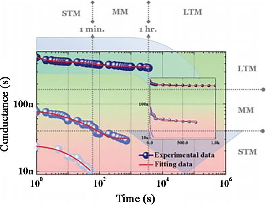
Author's personal copy
8724                                                                                            J Mater Sci (2018) 53:8720–8746

Table 1 Summary of RRAM stack, electrodes and switching layer

               Structures                                    Switching      Model
                                                             behavior

RRAM stack
Symmetric   Symmetric structure:                             Mainly         Thermal dissolution model:
 and        (e.g., Pt/NiO/Pt [25], Pt/TiO2/Pt [26], Pt/       unipolar      Oxygen ions accumulated near the anode during the SET.
 asymmetric   ZrO2/Pt [27], Pt/HfO2/Pt [28])                  switching       The Joule heating activates O2- to combine with oxygen
                                                                              vacancies during the RESET and rupture of conductive
                                                                              filaments (CFs)
               Asymmetric structure:                         Mainly         Ionic migration model:
               (e.g., Pt/TiO2/TiN [29], TiN/ZnO/Pt [30],      bipolar       Oxide interfacial layer formation between electrode and
                 TiN/HfO2/Pt [31], Pt/NiO/Cu [32], Cu/        switching       oxide acts as oxygen diffusion barrier.
                 La2O3/Pt [33])
                        Structures                     Mechanism           Advantages

RRAM electrodes
Active and inert metal Active metal electrode:       ECM                   Active ? inert electrodes in RRAM exhibit better endurance
 electrode             Ti, Al, Ag, Cu, Ni, TiN, TaN, VCM                    and longer retention time
                         ZrNx, ITO                   Mainly bipolar
                                                      switching
                       Inert metal electrode:        VCM
                       Pt, Au, Ru, Pd                Mainly unipolar
                                                      switching
                       Novel electrodes:                                   n ? -Si: self-rectifying property which is capable of
                       CNT [34, 35] n ? Si [36]                             alleviating cross talk issues
                         graphene [37]                                     Graphene and carbon nanotube electrodes: ultradense
                                                                            memories.

          Structures                  Mechanism                                       Advantages

RRAM switching layer
Doping Dopants: Ti [20], Ge [21]     Forming-free: Dopants diffuse into oxide layer Good data retention, potential multi-bit operation,
                                      and oxygen vacancies are increased               highly scalable property and fast switching
                                                                                       speed
                                                                                      Better uniformity (temporal fluctuations) (cycle
                                                                                       to cycle) and spatial fluctuations (device to
                                                                                       device)
Bilayer   One layer with lower       Resistive switching occurs at higher resistivity Low power consumption
           resistivity and one with   layer, and the lower resistivity layer can      Lower RESET current
           higher resistivity         improve the resistance of the ON state          Better uniformity (diffusion of metal ions from
          E.g., TMO1/TMO2 [24],                                                        the lower resistivity to the higher resistivity
           Ni/GeOx/HfOx/TaN [38],                                                      layer. This stabilizes the CFs to reduce the
           MoOx/GdOx [39]                                                              randomness of resistive switching (RS)
Multi-    E.g., Pt/HfOx/TiOx/HfOx/                                                    Multi-level storage function
 layer     TiOx/TiN [40]., Pt/Ta2O5/
           TiOxNy/TiN/Ta5/Pt [41]

chip design. When compared with other types of                        MRAM. In addition, the non-volatile property of
synaptic device, RRAM possesses the advantages of                     RRAM outweighs the traditional DRAM which
high endurance that FLASH memories do not offer,                      requires constant recharging [82–87]. Table 3 lists out
lower programming energy and smaller cell size than                   some of the leading institutions and industries using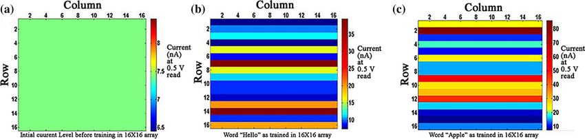
Author's personal copy
J Mater Sci (2018) 53:8720–8746 8725
Table 2 Conduction mechanism analysis
Mechanism Remarks
P-F emission (field-assisted Thermal excitation of electrons emits from traps into the conduction band of the dielectric.
thermal ionization) In(1/V) - V1/2
SCLC (space charge limited When electric field is high, the current is dominated by the charge carrier injected from the electrode.
current) The current is only dependent on the mobility rather than the charge-carrier density.
I–V2
Conductive filament Formation and rupture of conductive filaments
I–V
Not proportional to electrode area
Electrode limited Relevant to electrode (materials, area)
Schottky emission Thermal excitation of electrons emits over the barrier into the conduction band of the dielectric.
Direct tunneling Electron tunnels from cathode to anode directly
Thin film thickness less than 3 nm
Fowler–Nordheim (F-N) tunneling Electron tunnel from cathode to conduction band directly
High voltage
power consumption. RRAM is touted as a possible
solution and has been studied by Nanoelectronics
and Nanotechnology Research Group from Stanford
University and NanoST laboratory from National
Chiao Tung University [89–92]. The results showed
that RRAM possesses similar performance as that of
PCRAM and consumes less power to operate artifi-
cial synapse [93–95]. Since then, RRAM has attracted
massive attention from numerous academic institu-
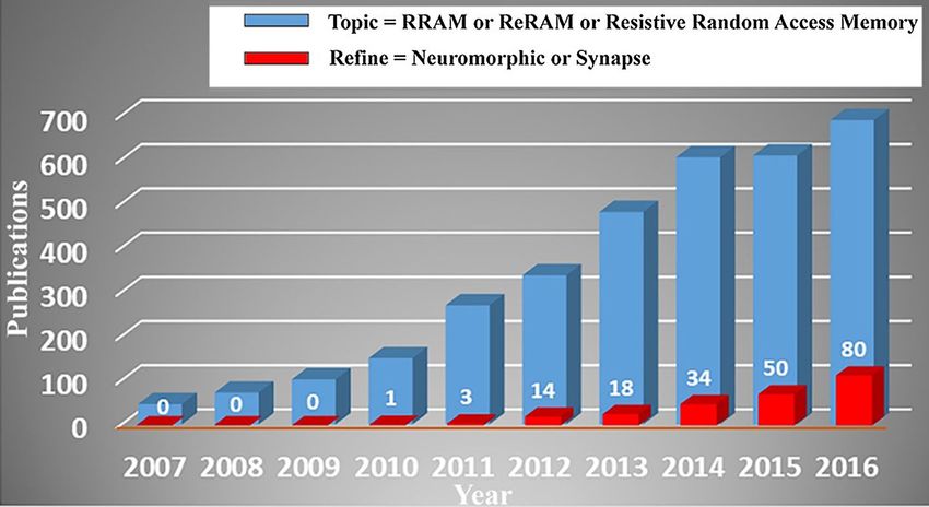
tions. From Fig. 5, the number of publications on
RRAM has increased by 14 times in the last decade.
Among these publications, the proportion of papers
demonstrating neuromorphic computing applica-
tions has increased every year since 2010. In 2016,
Figure 4 Interconnectivity in neuronal circuit. nearly 11% of papers presented RRAM’s applications
in the neuromorphic system. In general, most of
resistive memories as synaptic devices. Phase change studies on RRAM involve oxide materials. Oxide-
memory (PCM) has shown great potential for neu- based RRAM is attractive as the underlying metal
romorphic computing in the Synapse project per- insulator–metal structure is simple, compact and
formed by leading researchers from IBM (TrueNorth) CMOS-compatible. Most importantly, the multi-level
[88]. However, the greatest drawback is its high behavior needed to imitate adaptive synaptic changes
Table 3 Active players in the resistive memory of the synaptic devices (with to Ref. [97])
Project performer Synaptic device Device structure Scale Synaptic characteristics Application
GIST RRAM TiOx/HfOx Unit cell Multi-level cell Visual cortex
LETI CBRAM Ag/GeS2 8 9 8 1T1R N/A Human Cochlea and Retina
Stanford PCM GST 10 9 10 1T1R Yes Pattern recognition
POSTCH RRAM Pr1-xCaxMnO3 11 k Array Yes Signal recognition
IBM PCM Ge2Sb2Te5 165 K Array N/A Pattern recognition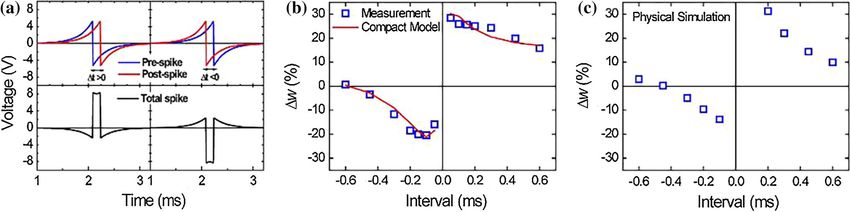
Author's personal copy
8726                                                                            J Mater Sci (2018) 53:8720–8746

Figure 5 Publications per
year from 2007 to 2016. The
data is from the web of science
site (www.webofknowledge.
com). The search expression
for blue bars is Topic = ‘‘R-
RAM’’ or ‘‘RRAM’’ or ‘‘Re-
sistive random-access
memory’’. The data for red
bars are from subsequent
refined with expressions
Refine = ‘‘neuromorphic’’ or
‘‘synapse’’.

has been found in many oxide-based RRAM devices.          connection strength between pre- and postsynaptic
In addition, the energy per synaptic operation can be     neurons. The process of adjusting the strength of
made as low as sub-pJ and the programming current         these interneural connections is known as synaptic
can reach below 1 lA [96]. In this review, we will        operation. The number of synaptic operations of a
focus on oxide-based RRAM memristor device as a           neuromorphic chip is strongly dependent on the
synapse in the neuromorphic system.                       intrinsic properties of the materials used as the
  The basis of learning and formation of memory are       synapse. This will further determine the lifetime of
the modification of synapse connections as a result of    the chip or its availability for learning process. The
accumulated experience, the feature known as              required cyclability (number of synaptic operations)
synaptic plasticity. So far, synaptic plasticity had      of the chip will depend on the expected lifetime and
been widely studied their correlation in learning and     operation frequency of the chip. If the chip is expec-
memory [98–100]. Hebbin’s rule postulates that            ted to be available for learning for about 10 years
changes at synapses within the brain underlie learn-      under 100 Hz of operation frequency, the chip must
ing and memory, which was proposed by Donald              be able to execute at least 1010 synaptic operations.
Hebb in 1949 [101]. It provides an algorithm to           RRAM device has been reported to achieve endur-
update weight of neuronal connection within neural        ance of as high as 1012; thus, it emerges as one of the
network and a physiology-based model to reproduce         strongest candidates for the development of highly
the activity-dependent features of synaptic plasticity.   reliable neuromorphic chip. The feasibility of RRAM
In biology, excitatory and inhibitory postsynaptic        device for synapse applications was first demon-
potentials are transmitted between neurons through        strated in 2010 by Jo et al. [53]. According to the
chemical and electrical messaging at synapses, driv-      experimental RRAM STDP curve as shown in Fig. 6,
ing the generation of the new action potentials           conductance increases with the time delay when the
(spikes). In RRAM-based neuromorphic approaches,          presynaptic spikes precede the postsynaptic spikes
the tunable resistive state of RRAM functions as          (t \ 0). Conversely, the decrease of conductance
synaptic weight in the neuromorphic system. The           occurs when the postsynaptic spikes precede the
weight of synapse could be manipulated by changing        presynaptic spikes (t [ 0). In addition to the rise/fall
the resistance states in RRAM devices, which follows      of synaptic weight, the change of synaptic weight
the rule of spike-timing-dependent plasticity (STDP)      could also be either long term or short term. Upon
[102–104]. STDP is a form of synaptic plasticity that     changing the spike rate, Ohno [105] demonstrated
adjusts the strength of the connection between the        both the long-term potentiation and short-term
presynaptic neuron and postsynaptic neuron based          potentiation in Ag2S-based RRAM device. Long-term
on the relative timing of its output and input action     potentiation refers to the persistent increase in
potentials (electric pulses). In the implementation of    synaptic strength which lasts minutes or more, while
STDP learning rule, it requires the adjustment of the     short-term potentiation refers to the transiently
Author's personal copy
J Mater Sci (2018) 53:8720–8746                                                                             8727

                                                            Oxide-based RRAM for neuromorphic
                                                            computing application

                                                            Resistive switching behavior had been observed in
                                                            many oxides, while most of them are transition
                                                            metals. Some of them had been explored for neuro-
                                                            morphic application and summarized in the periodic
                                                            table (Fig. 8). We selected PMCO, HfOx, TaOx, TiOx,
                                                            NiOx, AlOx, WOx and other oxides for discussion in
                                                            this article as their property and application for
                                                            neuromorphic computing were well investigated.
                                                            The growth techniques of RRAM oxide materials
                                                            include traditional deposition methods, i.e., sputter-
                                                            ing, atomic layer deposition (ALD) and pulsed laser
Figure 6 Experimental RRAM STDP curve. (Reprinted with      deposition (PLD). In addition, novel methods for
permission from Ref. [53].).                                RRAM fabrication have also been reported. The tra-
                                                            ditional and novel methods for RRAM are listed in
enhancement of synaptic strength which acts on a            Table 4.
timescale of tens of milliseconds to a few minutes.
The results showed that the RRAM device exhibits            Pr12xCaxMnO3 (PCMO)-based synaptic
short-term potentiation behavior with the applied           devices
pulse width at 0.5 s and interpulse delay at 20 s. As
shown in Fig. 7, the potentiation of synaptic weights       Pr1-xCaxMnO3 (PCMO), as representative materials
is volatile and no permanent change was observed            in perovskite transition metal oxide, has been widely
after nine pulses. However, when the interpulse             employed as synaptic devices. Its resistive switching
delay was reduced by 10 times, 6 pulses are sufficient      property was first discovered by Asamitsu et al. in
to induce the stable potentiation and permanent high        late 1990 [135], which draws the attention from aca-
conduction state remains thereafter. In general, short-     demies on complex transition metal oxide for RRAM
term and long-term plasticity could be mimicked in          device [136, 137]. The resistive switching of PCMO is
the single synapse by tuning the non-overlapping            based on metal–insulator (MIT) mechanism. MIT is a
spike rate. This synaptic plasticity plays a crucial role   kind of valence change system, in which the electrons
in the way the brain implements learning and                are injected into the insulator layer to conduct the
memory. Therefore, the rule of STDP (Fig. 7) is con-        current with an external applied field. In PCMO, the
sidered as one implementation of Hebbian learning.          injected electronic charge distorts the superlattice
                                                            structure and the mixed valence band behavior, a

Figure 7 a Short-term
potentiation and b long-term
potentiation of Ag2S-based
devices are induced for
different spike rates.
(Reprinted with permission
from Ref [105].).
Author's personal copy
8728 J Mater Sci (2018) 53:8720–8746
Figure 8 The periodic table of the elements highlighted with the host metal of RRAM materials and those had demonstrated for
neuromorphic computing.
Table 4 Summary of RRAM
device fabrication methods RRAM device deposition methods
Traditional methods Sputtering [106–113]
Atomic layer deposition [23, 114–117]
Pulsed laser deposition [118–122]
Plasma enhanced chemical vapor deposition [123–125]
Chemical synthesis particle ? spin-coating [126–128]
Sol–gel [129–132]
Novel methods Shattering process using an atomic force microscopy (AFM) tip [133]
Semi-auto screen printer [134]
process similar to ion doping processes. In addition, studied to optimize the device electric performance
PCMO is LRS active materials in which the SET [141]. Similarly, to avoid an abrupt LTD, a two-
operation is associated with reverse biasing, while PCMO-memristor device model was proposed by
RESET operation occurs at forward biasing. Moon et al. [142]. In 2015, a circuit capable of realiz-
In 2012 and 2013, Park [138, 139] demonstrated ing the learning process was designed and published
1-kbit cross-point array neuromorphic system based [143]. In the same year, a high-density PCMO cross-
on PCMO synaptic devices. The HRS is achieved point synapse array on the 8-inch wafer was fabri-
with the applied positive bias when the oxygen ions cated. The proposed system had been demonstrated
are attracted from the PCMO layer, thus forming a to recognize human thought patterns for three vow-
thicker oxide layer with Al electrode. The continu- els [97]. In addition, vivo experiment had also been
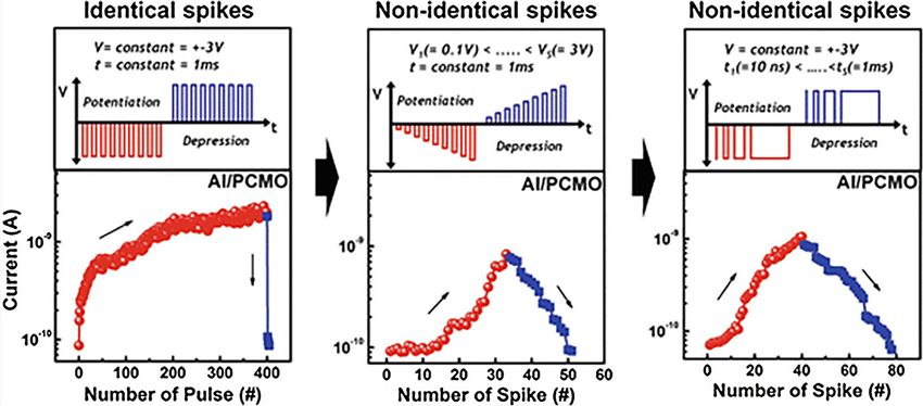
ously increasing potentiation and depression behav- performed by the group. In the paper, the PCMO-
iors were found when the identical spikes (pulses based nanoscale analogy synapse device was suc-
with same amplitude and width) were applied. In cessfully applied for neural fear-conditioning signal
order to overcome the difficulty in achieving gradual recognition on a live rat. In 2016, Moon, K from
long-term depression (LTD) caused by asymmetry Hwang, H group reported PCMO-based interface
potentiation/depression, a new programming switching device with 5-b MLC (32 levels) and
scheme was developed [140]. The growth process improved data retention by using Mo electrodes for
control of PCMO device with TiN electrode was the neuromorphic system [144]. The Mo/PCMOAuthor's personal copy
J Mater Sci (2018) 53:8720–8746 8729
synapse array has experimentally confirmed with the HfOx-based synaptic devices
realization of pattern recognition with high accuracy
when working with NbO2 oscillator neuron [145]. In HfOx materials have been widely used in RRAM
2017, a comprehensive study of PCMO-based materials because of its excellent CMOS compatibil-
synaptic devices had been reported in the book ity. In industries, HfOx has been employed as a high-
‘‘Neuro-inspired Computing Using Resistive Synap- k dielectric for the gate insulator of CMOS MOSFETs.
tic Devices’’ [146]. The PCMO synapse performance is In HfOx-based RRAM device, TiN is usually applied
evaluated in 1-kb and 8-kb crossbar arrays. The as an electrode. TiN functions as an oxygen scav-
interfacial-type PCMO RRAM was demonstrated enger that depletes the O atom from HfOx thin film
with wide on/off ratio (104), extremely stable analogy and functions as an oxygen reservoir. It has been
resistance changes and low LRS current (1 lA) when reported that HfOx RRAM has a large on/off ratio
device scales down to 150 nm. The influence of active ([ 102), high endurance ([ 106), retention, multi-bit
electrode, nitrogen treatment and extra insulating storage and high-speed operation (\ 10 ns) [142–146].
layer (AlOx) has also been investigated. The synaptic In 2011, a novel electronic synapse of HfOx/AlOx-
performance of PCMO is evaluated as shown in based memory was presented by Yu et al. The
Fig. 9, where the potentiation and depression with structure showed attractive features such as reduced
identical and non-identical spikes are displayed. It is randomness of resistive switching, multi-level
observed that the gradual switching of depression is switching and the capability to modulate resistances
only triggered by non-identical spikes, which is based on the input pulse amplitudes, suggesting
accounted for the high asymmetry ratio of potentia- great potential to use in emerging neuromorphic
tion/depression conduction. computation system [147]. In 2012, the same group
So far, PCMO is one of the most matured RRAM reported HfOx-based RRAM device application in the
materials for neuromorphic computing. It possesses neuromorphic visual system. At the system level, a
various advantages: nanoscale device dimension neuromorphic visual system consisting of 1024
(150 nm), multi-level states (5-b MLC), retention, CMOS neuron circuits and 16,348 RRAM synaptic
uniformity (STD(r)/Iave \ 0.5), on/off ratio (104) and devices was fabricated. The system exhibited great
high-density crossbar array structure (8 kb) [146]. performance in image orientation selectivity and high
However, further improvement of symmetric weight tolerance on temporal and spatial variability. After
update is still required. one year, Gao, B [148] and his coworkers developed a
method to achieve gradual switching on the setting
process in TiN/HfOx/Pt devices. To avoid the gen-
eration of random and avalanching oxygen vacancies
Figure 9 Potentiation and depression with various programming spikes: identical and non-identical spikes, reprinted with permission
from Ref. [146].Author's personal copy 8730 J Mater Sci (2018) 53:8720–8746 (VO) clusters, the team developed a methodology by and depression processes using an easily imple- doping trivalent elements into HfOx layer. The local mentable algorithm based on a train of identical formation energy of VO near the dopants was pulses [153]. The impact of HfOx-based synapses reduced, and VO will distribute more uniformly in cycle to cycle (temporal) and device to device (spa- the conductive filament region. The fabricated TiN/ tial) variability on the convolutional neural network Gd:HfOx/Pt devices have also shown controllable was investigated by Garbin, D [154]. The results multilevel resistive switching behavior. Garbin [149] showed that the convolutional neural network (CNN) applied pulse-train schemes to a 3 bit per cell HfO2 architecture has a high tolerance to the variability. RRAM in 2014, causing the relative standard devia- Lee et al. [155] proposed a silicon-based charge trap tions of resistance levels to improve up to 80% com- memory with Al/HfO2/Al2O3/Si3N4/Si structure. pared to the single-pulse scheme. In the same year, The device implemented both short-term plasticity Benoist, A integrated TiN/HfO2/Ti/TiN RRAM with and long-term potentiation in the synapse. The use of an advanced 28-nm CMOS process [150]. A global HfO2-based oxide-based resistive memory (OxRAM) overview of HfO2 material performances was asses- devices operated in a binary mode to implement sed on a statistical basis, and projection for larger synapses in a CNN was also studied by Garbin, D in array integration was discussed. The influence of Cu 2015 [149]. The proposed HfO2-based OxRAM tech- dopant was investigated by Tingting, G., and it was nology offers good electrical properties including found that Cu-doped HfO2-based RRAM has high endurance ([ 108 cycles), fast speed (\ 10 ns) improved resistive switching with multilevel storage and low energy (\ 10 pJ). High accuracy (recognition [151]. The application of Mn-doped HfO2-based rate [ 98%) was demonstrated for a complex visual RRAM has demonstrated speech recognition by pattern recognition application. Covi, E proposed Mandal [3]. A comparison between a 20-nm times TiN/HfO2/Ti/TiN memristor as artificial synapse 20-nm sized synaptic memory device with that of a for neuromorphic architectures. The collected STDP state-of-the-art VLSI SRAM synapse has exhibited 103 data were used to simulate a simple fully connected reduction in area and 106 times reduction in the spiking neural network (SNN) for pattern recognition power consumption per learning cycle. The colormap [156]. An innovative approach for real-time decoding for speech recognition of words ‘‘Hello’’ and ‘‘Apple’’ of brain signals based on SNN was presented by is shown in Fig. 10. Werner [157]. HfOX-based RRAM devices were used In 2015, Wang presented a new artificial synapse to implement synapse and SNN, enabling the net- scheme, consisting of a HfOx RRAM memristive work for autonomous online spike sorting of mea- switches connected to 2 transistors responsible for sured biological signals. The system allows real-time gating communication and learning operations. learning and completely unsupervised operation. The STDP was achieved through appropriate shaping of real-time functionality, low power consumption (10 the presynaptic and the postsynaptic spikes [152]. nW) and high recognition rate 90% of the system Covi, E demonstrated the Al:HfO2 memristor device make it a great candidate for future healthcare use for artificial synapse, emulating the potentiation applications. HfOx-based synapses were used in SNN Figure 10 Synaptic weights. a Initial current level. b The con- when the word ‘‘Apple’’ trained on the crossbar array of synaptic ductance distribution when the word ‘‘Hello’’ trained on the devices. Reprinted with permission from Ref. [3]. crossbar array of synaptic devices. c) The conductance distribution
Author's personal copy
J Mater Sci (2018) 53:8720–8746                                                                              8731

for real-time unsupervised spike sorting of complex      conductance and state fluctuation [160]. In the report,
brain signals. Synaptic weights are modulated            a physics-based compact model was also proposed
through the application of an online learning strategy   for facilitating circuit-level design. Based on previous
inspired by biological STDP. According to the report     studies, the group successfully applied 3D two-lay-
by Wang et al. [158] this network had been tested by     ered Ta/TaOx/TiO2/Ti cross-point synaptic array to
real spiking data from the in vitro preparation of the   implement highly anticipated hardware neural net-
crayfish sensory-motor system. The proposed RRAM         works (HNN) in 2016 [161]. In total, more than 50
was validated by different sets of real biological       analogue synaptic weight states were controlled with
spiking data without parameter tuning (e.g., the         minimal drifting during a cycling endurance test of
threshold level for spike detection). This artificial    5000 training pulses. The team also proposed a new
SNN is able to identify, learn, recognize and distin-    state-independent         bipolar-pulse-training      (BP)
guish between different spike shapes in the input        scheme, and this scheme significantly improved the
signal with a recognition rate about 90% without any     nonlinearity of weight updates, consequently
supervision.                                             improving the training accuracy.
   HfOx is a superior RRAM material and the HfOx-           Similarly, Ta/TaOx/TiO2/Ti synaptic devices were
based synaptic device has demonstrated its applica-      also reported by Gao et al. [162]. The device is
tion in neuromorphic computing, such as speech or        forming-free, and more than 200 levels of conduc-
pattern recognition. Gradual switching in the SET        tance states could be continuously tuned by identical
process can also be achieved through doping with         programming pulses. In addition, the team proposed
trivalent metals, enabling the high-density              a novel fully parallel write and read scheme to
applications.                                            accelerate the weight update and increase energy
                                                         efficiency in the training process on the chip. In order
TaOx-based synaptic devices                              to engineer the conduction modulation linearity,
                                                         Wang et al. [163] proposed a new approach in 2016
TaOx-based synaptic devices have also attracted          where a diffusion limiting layer (SiO2) is inserted at
much attention. TaOx switching layer in an RRAM          the TiN/TaOx interface. The device exhibited higher
device usually consists of two phases: TaO2 phase        switching linearity and lower power consumption
which is more conducting and Ta2O5 phase which is        that is desirable in neuromorphic computing hard-
more insulating. The TaOx RRAM has been reported         ware. Recently, Pt/Ta2O5-x/W devices fabricated
to possess high endurance ([ 1012 cycles), and its       using vertical 3D architectures were demonstrated by
application in neuromorphic computing has been           Wang [164]. The proposed memory can be recovered
well demonstrated. TaOx could be engineered in           with a timescale when the electrical stimulation was
synaptic device alone or combined with another           removed. This recoverable process can emulate the
oxide (TiO2) layer in MIM structures. In this section,   synaptic plasticity including rapid decay and slow
both single-layer TaOx or multi-layer TaOx-based         decay stages of forgetting in the memory loss process
synaptic devices will be discussed.                      of the human brain. Yao, P and his coworkers
   Wang reported a high-density 3D synaptic archi-       reported face classification using electronic synapses
tecture based on Ta/TaOx/TiO2/Ti RRAM with               of TaOx/HfAlyOx-based RRAM devices [165]. This
ultralow sub-10 fJ energy per spike for neuromorphic     optimized device structure has shown bidirectional
computation in 2014 [159]. In addition, the analogue     continuous weight modulation behavior. A neuro-
synaptic plasticity was simulated using the physical     morphic network is developed using analogue
and compact models to facilitate future neuromor-        1024-cell-1T1R RRAM array, and its application in
phic system designs. Thereafter, Wang et al. further     grayscale face classification has been experimentally
investigated the synaptic device with the same           demonstrated with parallel online training. The
structure experimentally and theoretically. The          energy      consumption       in    each    iteration   is
results showed that the device can be used for           1000 9 (20 9) smaller than the Intel Xeon Phi pro-
implementing concurrent inhibitory and excitatory        cessor with off-chip memory.
synapses (Fig. 11). In addition, the devices also pro-      From our literature review, bilayer stack TaOx/
vided superior performances as compared to typical       (HfAlyOx, TiOx) is intentionally designed as a
filamentary synaptic devices in reducing synaptic        synaptic device in the application of neuromorphic
Author's personal copy
8732 J Mater Sci (2018) 53:8720–8746
Figure 11 Spike-timing-dependent plasticity (STDP). a Biomor- (Dw) was positive for Dt [ 0, whereas it was negative for Dt \ 0.
phic-action-potential-like waveforms used for STDP measurement b The measured Dw as a function of Dt for the Ta/TaOx/TiO2/Ti
and simulation. The prespike pulse was applied to the Ta electrode, device. The red line shows the fitting result of using the physics-
and the postspike pulse was applied to the Ti electrode. The based compact model. c Simulation results for STDP, obtained by
potentiation and depression actions were controlled by the relative considering oxygen ion migration and the homogeneous barrier
timing of the pre- and postspikes (Dt). The synapse weight change modulation model. Reprinted with permission from Ref [160].
computing. The possibility of engineering the TaOx- amorphous–crystalline interfaces in TiOx/TiOy
based RRAM array in 3D structure enables the RRAM structures for enhanced resistive switching
emulation of the high-density synaptic network in the and synaptic properties [168]. A physical model was
real biological system. also proposed to divulge the crucial role of temper-
ature, electric potential and oxygen vacancy density
TiOx-based synaptic devices on the switching effect. An 8 9 8 array of the neuron
on a standard 6 M 180 nm of CMOS process as part
TiOx is one of earliest materials found to exhibit of a larger multi-purpose neuromorphic chip was
resistive switching property. In the previous section, demonstrated by Mostafa, H as shown in Fig. 12
TaOx/TiOx bilayer structure RRAM for synaptic [169]. The proposed CMOS-memristor system com-
application has been introduced. Here, we will dis- prises of CMOS neurons interconnected through TiOx
cuss other multi- and single-layer TiOx-based memristors and spike-based learning circuits which
synaptic devices. modulate the conductance of the memristive synapse
In 2011, the synaptic performance of TiO was elements according to a spike-based perceptron
explored by Seo [46], demonstrating that TiOx and plasticity rule. In 2016, Park developed a Mo/TiOx-
TiOy bilayer RRAMs exhibit analogue property based interface RRAM and proposed a hybrid pulse
where the multilevel conductance states were caused mode for the synaptic application [170]. The TiOx-
by the movement of oxygen ions between the two based device is capable of producing 64-level con-
TiOx phase. The STDP was demonstrated by apply- ductance states, and the proposed hybrid pulse mode
ing 100 successive identical pulses for potentiation or improves the symmetry of conductance change
depression of synaptic weight. A year later, Yu under both potentiation and depression conditions.
developed TiOx/HfOx/TiOx/HfOx multi-layer The neural network simulation has shown that the
RRAM stacks exhibiting more gradual and smooth hybrid pulse mode can enhance the pattern recogni-
RESET switching for synaptic devices [166]. Short tion accuracy of the proposed TiOx stack.
pulses (10 ns) with an identical pulse amplitude Although extensive investigations have been car-
enabled a sub-pJ energy per spike with potentially ried out on switching mechanism of TiOx RRAM, the
simple neuron circuits. Berdan emulated short-term demonstration of TiOx RRAM for neuromorphic
synaptic dynamics with TiO2 memristive devices in computing is still limited when compared to the
2015 [167]. The meta-stable memory transitions in above-mentioned PCMO, HfOx, TaOx materials. In
TiO2 RRAM devices have proved to be the key fea- most situations, TiOx is used in conjunction with
ture to capture short-term synaptic dynamics. In bilayer or multi-layer synaptic device to optimize the
addition to Seo, K works on bilayer TiOx/TiOy performance.
RRAM structure in 2011 [46], Bousoulas, P studiedAuthor's personal copy
J Mater Sci (2018) 53:8720–8746 8733
potentiation behavior was emulated by the increase
in memristor’s conductance when applying the elec-
trical pulses. In addition, spontaneous conductance
decaying toward its initial state resembles the
synaptic long-term potentiation. Finally, an artificial
neural network was constructed to realize the Pav-
lov’s dog model (Fig. 13).
WOx-based synaptic devices
Tungsten oxides (WOx) are another great candidate
for memristive devices as a bio-inspired artificial
synapse. The advantage of WOx-based synaptic
devices includes accredited endurance (105 cycles),
CMOS compatibility and memorization and learning
functions. Here, we highlight the implementation of
this material in neuromorphic computing as a bio-
logical artificial synapse.
Synaptic behaviors and modeling of a WOx mem-
Figure 12 a Micrograph of the multi-purpose neuromorphic chip
ristive device were reported by Chang [174] .The Pd/
die showing the neuron tile array and the bias generator.
WOx/W-structured memristor device shows reliable
b Illustration of the hardware setup used to obtain measurements
in this paper. The presynaptic terminal of one neuron tile is
synaptic operations with good endurance. The
connected to the postsynaptic terminal of another neuron tile synaptic devices can endure at least 105 potentiation/
through an off-chip TiO2-x memristor. A PC controls the digital depression pulses without degradation. Furthermore,
settings of the on-chip bias generator. Reprinted with permission the memristor behavior was explained by a novel
from Ref. [169]. model that takes both drift and diffusion effects into
consideration. Figure 14 presents the retention loss
NiOx-based synaptic devices
Similar to TiOx, NiOx is one of earliest materials
found to exhibit restive switching behavior. Although
NiOx-based RRAM devices have been reported with
high endurance (106) and retention, its application for
neuromorphic computing is restricted due to the
poor uniformity. A bipolar NiOx RRAM, two NMOS
FET and a capacitor were used to fabricate analogue
synaptic devices (circuits) by Akoh [171]. This device
also has the ability to update the synaptic conduc-
tance according to the difference of pre- and post-
neuron spike timing. In 2013, Hu emulated the
paired-pulse facilitation of biological synapse with
NiOx-based memristor, thus creating a form of short-
term synaptic plasticity [172]. It was also observed
that the current in NiOx-based memristor had
increased after a second electrical pulse. Addition-
ally, the magnitude of the facilitation decreases with
the pulse interval and it increases with the pulse
magnitude or pulse width. Hu, S.G and his cowork-
ers realized the well-known Pavlov’s dog model with Figure 13 Learning and forgetting of association in Pavlov’s dog
experiment realized with the three-neuron neural network.
NiOx-based memristor [173]. The long-term
Reprinted with permission from Ref [173].Author's personal copy
8734 J Mater Sci (2018) 53:8720–8746
Figure 14 a DC I–V curves
of a memristor studied.
b Schematic illustration of
oxygen vacancy diffusion.
c Retention loss curve of Pd/
WOx/W-based memristor.
d Forgetting memory of
human memory curve.
e Schematic illustration of
synaptic plasticity modulation.
Reprinted with permission
from Ref [47].
curve and forgetting memory in a human memory neuromorphic computing, enhancement of synaptic
curve from a paper by Chang [47]. It was found that operation time (endurance) is of importance.
the trend of retention curve of a Pd/WOx/W-based
memristor and human forgetting curves greatly cor- AlOx-based synaptic devices
respond to each other and both can be fitted using a
stretched-exponential function (SEF). In addition, the The resistive switching behavior in AlOx was first
temperature and humidity impact on the perfor- reported by Hickmott [1]. AlOx is of interest in
mance of a WOx memristive device was studied by RRAM materials due to its large band gap (* 9 eV)
Meng et al. and Yong et al., respectively [175, 176]. and low RESET current (* lA). For neuromorphic
According to the simulation results, the synaptic application, AlOx can also be used alone or stacked
weight of WOx memristive device decays faster as the with other RRAM materials to improve the unifor-
temperature increases due to higher oxygen vacan- mity of the synaptic device characteristics.
cies diffusion. In addition to the temperature, the AlOx-based resistive switching device was inves-
memristive effects of tungsten oxide are also highly tigated by Wu [49] to serve as a potential electronic
humidity dependent. The adsorbed moisture on the synapse device. The 0.48 lm 9 0.48 lm Ti/AlOx/
surface of WO3 has resulted in decreasing conduc- TiN memory stack exhibited multi-level resistance
tances as the H cation induces an increase in barrier states when varying the compliance current levels or
heights. the applied voltage amplitudes during pulse cycling.
Among other transition metal oxides, WOx is a In his work, around 1% resistance change per pulse
great candidate material for synaptic devices appli- cycling was obtained and an STDP realization
cation. For further exploring its application in scheme was proposed to implement the synaptic
device in large-scale hardware neuromorphicAuthor's personal copy
J Mater Sci (2018) 53:8720–8746 8735
computing system. In 2015, Prezioso experimentally Wang, C.H et al. reported the synaptic behavior of a
characterized Al2O3/TiO2-based memristors to FeOx-based RRAM in which the dependence of
modulate the impact of conductance-dependent compliance current on conductance stability was
conductance change on short-term dependent plas- studied [179]. The application of CeO2-based RRAM
ticity [177]. The utilization of TiOx/Al2O3-based for highly energy efficient neuromorphic systems
memristor devices to emulate biological synaptic was demonstrated by Kim et al. The Pt/CeO2/Pt
behavior for building brain-inspired computers was device exhibited the polarity-dependent and asym-
explored by Banerjee, W.et al. in 2017 [178]. The metric diode-type resistive switching [180], and the
proposed TiO2/Al2O3 synaptic device has the capa- detailed switching characteristics of artificial synap-
bility to switch from short-term memory (STM) to ses (potentiation and depression) were discussed.
long-term memory (LTM) by introducing a mezza- A GdOx and Cu-doped MoOx stack with a platinum
nine state at medium memory (MM) as shown in top and bottom electrodes were reported by Choi
Fig. 15. In the paper, the dependence of retention [45]. The weighted sum operation was carried out on
(decay time) on conductance levels (memory level) electrically modifiable synapse array circuit based on
was investigated and an experimentally proven the proposed stacks [181]. The biological synaptic
psychological model is presented. behavior was demonstrated by Chang through inte-
Till now, the potential validity of Al2O3 materials grating SiOx-based RRAM with Si diodes. The pro-
for electronic synapses had been experimentally posed one-diode-one-resistor (1D-1R) architecture
demonstrated. Nevertheless, the reports of sophisti- not only avoids sneak-path issues and lowers
cated Al2O3-based memristor as an artificial synapse standby power consumption, but also helps to realize
are limited. Therefore, further verification with dif- STDP behaviors [182]. VOx is a well-known Mott
ferent structures is required. material which experience sharp and first-order
metal-to-insulator transition (MIT) at the around
Other oxide-based synaptic devices 68 °C [183]. The application of VOx as RRAM mate-
rials had been explored by Drisoll et al. [184] through
Besides the materials discussed above, a variety of sol–gel technique. Nevertheless, most researches on
other materials has been studied to implement neural VOx so far focus on its use for select device which can
network as a synaptic device. FeOx-based RRAM be integrated with RRAM device to mitigate sneak-
with mixed-analogue–digital behavior was investi- path current. The Pt/VO2/Pt selector has been inte-
gated by Deng et al. [12] for a recurrent neural net- grated with NiO unipolar RRAM by Lee et al. [185] in
work using the recursive least-squares algorithm. 2007 and ZrOx/HfOx bipolar RRAM by Son et al.
[186] in 2011. In 2016, 1S1R configuration of W/VO2/
Pt selection device and Ti/HfO2/Pt RRAM was
demonstrated by Kailiang et al. [187]. However,
thermal instability is a major challenge for VO2 for
practical applications [14].
Summary and outlook
In conclusion, we have outlined an overview of
oxide-based RRAM materials for the applications in
neuromorphic computing. Table 5 summarizes the
RRAM materials and their parameters discussed in
this review. Our work suggested that the neuromor-
phic approach with oxide-based RRAM devices is
promising. So far, PCMO, HfOx, TaOx, TiOx, NiOx,
Figure 15 Memory effects in the TiOx/Al2O3-based electronic
synaptic junction. The figure shows the conductance failure with
WOx, AlOx, etc., materials have been demonstrated
time. A linear scale plot is shown in the inset of the figure. for their application in oxide-based synaptic devices.
Reprinted with permission from Ref [178]. However, challenges still remain in specific materials,Author's personal copy
8736 J Mater Sci (2018) 53:8720–8746
Table 5 Summary of RRAM materials in this review
Material On/ Endurance Energy Multi- Switching Neuromorphic computing applications
off consumption levels time
ratio
PCMO 103 105 6 pJ 32 8 ns Pattern recognition
[97, 136–146] Human thought patterns
Neural fear-conditioning signal recognition
HfOx 102 106 10 pJ 8 10 ns Speech recognition
[147–151] Visual pattern recognition
TaOx 10X 1012 10 fJ 200 105 ps Grayscale face classification
[158–164]
TiOx 105 2 X 10⁶ sub-pJ 64 5 ns Pattern recognition in simulation
[46, 166–170, 189]
NiOx 106 106 – 5 20 ns Learning and forgetting of association in Pavlov’s
[171–173, 185, 190, 191] dog experiment realized.
WOx 103 105 – 8 50 ns Human forgetting curves
[47, 174–176, 192]
AlOx 106 105 1.5 pJ 10 10 ns Spike-timing-dependent plasticity realization
[49, 193–195] scheme.
FeOx 102 6 9 104 – 6 10 ns Long-term potentiation and long-term depression
[179, 196, 197] demonstration
CeO2 105 104 – 8 200 ns Synaptic potentiation and depression
[180, 198] characteristics demonstration
MoOx 109 106 – 8 1 ms Weighted sum operation carried out on MoOx-
[39, 199] based electrically modifiable synapse array
circuit
SiOx 107 106 – 4 100 ps Long-term potentiation and long-term depression
[182, 200–202] demonstration
e.g., poor symmetric weight update for PCMOx- high thermal conductivity which minimizes self-
based synaptic devices and low endurance for WOx- heating during operations and a large breakdown
based synaptic devices. In general, there are two field that might prevent the device from irreversible
main key challenges for overall oxide-based RRAM damages. In addition, MgO-based magnetic tunnel
materials. Although the inherent fault tolerance of junction memristors had been proposed for imple-
neural network models is able to mitigate the impact mentation of synapses [188]. Further research is
of device variation to some extent, the improvement required to expand the database of materials for
of spatial variation and temporal variation turns out synaptic devices and neuromorphic applications.
to be one of the greatest challenges on a long-term Finally, to implement oxide-based RRAM devices
basis. In addition, improvement of reliability char- as a synapse in neuromorphic systems, it is impera-
acteristics of the RRAM synaptic devices is another tive to have an in-depth understanding of the meta-
key challenge which is not well studied. plasticity mechanism and internal states of these
In future material research of neuromorphic com- memristive devices. The underlying mechanisms
puting applications, the study of novel tunable governing RRAM devices will inevitably be discov-
materials with enhanced properties for neuromor- ered from investigations of conduction and resistive
phic devices is one of the most exciting components. switching mechanism via results from either experi-
One such example is MgO, which has a large band ment or simulation. Further research work incorpo-
gap that ensures sufficient band offsets, a high rating interactions between materials, device levels,
dielectric constant that might potentially reduce circuit designs and computing processes will
leakage current (thus improving device scalability), aAuthor's personal copy
J Mater Sci (2018) 53:8720–8746 8737
certainly speed up the realization of oxide-based [8] Fackenthal R, Kitagawa M, Otsuka W, Prall K, Mills D,
RRAM synapses for neuromorphic systems. Tsutsui K, Javanifard J, Tedrow K, Tsushima T, Shibahara
Y, Hush G (2014) A 16 Gb ReRAM with 200 MB/s write
and 1 GB/s read in 27 nm technology. In: ISSCC digest
Acknowledgements technical papers IEEE international, vol 57, pp 338–339
[9] Luo Q, Xu X, Liu H, Lv H, Gong T, Long S, Liu Q, Sun H,
This work was supported by a RIE2020 AME-Pro- Banerjee W, Li L, Gao J, Lu N, Liu M (2016) Super non-
grammatic Grant (Neuromorphic computing, No. linear RRAM with ultra-low power for 3D vertical nano-
A1687b0033) and an Industry-IHL Partnership Pro- crossbar arrays. Nanoscale 8(34):15629–15636. https://doi.
gram (NRF2015-IIP001-001). WSL is a member of the org/10.1039/C6NR02029A
Singapore Spintronics Consortium (SG-SPIN). [10] Mertens R (2017) Digitimes. http://www.digitimes.com/
newregister/join.asp?view=Article&DATEPUBLISH=2017/
06/05&PAGES=PB&SEQ=200. June 08, 2017
References [11] Chang T-C, Chang K-C, Tsai T-M, Chu T-J, Sze SM (2016)
[1] Hickmott TW (1962) Low-frequency negative resistance in Resistance random access memory. Mater Today
thin anodic oxide films. J Appl Phys 33(9):2669–2682. 19(5):254–264. https://doi.org/10.1016/j.mattod.2015.11.
https://doi.org/10.1063/1.1702530 009
[2] Liu SQ, Wu NJ, Ignatiev A (2000) Electric-pulse-induced [12] Deng L, Li G, Deng N, Wang D, Zhang Z, He W, Li H, Pei
reversible resistance change effect in magnetoresistive J, Shi L (2015) Complex learning in bio-plausible mem-
films. Appl Phys Lett 76(19):2749–2751. https://doi.org/10. ristive networks. Sci Rep 5:10684. https://doi.org/10.1038/
1063/1.126464 srep10684
[3] Mandal S, El-Amin A, Alexander K, Rajendran B, Jha R [13] Advances and Trends of RRAM technology SemiconTai-
(2014) Novel synaptic memory device for neuromorphic wan (2015)
computing. Sci Rep. https://doi.org/10.1038/srep05333 [14] Wong HSP, Lee HY, Yu SM, Chen YS, Wu Y, Chen PS,
[4] Lee MJ, Park Y, Kang BS, Ahn SE, Lee C, Kim K, Xianyu Lee B, Chen FT, Tsai MJ (2012) Metal-oxide RRAM. Proc
WX, Stefanovich G, Lee JH, Chung SJ, Kim YH, Lee CS, IEEE 100(6):1951–1970. https://doi.org/10.1109/Jproc.
Park JB, Baek IG, Yoo IK (2007) 2-Stack 1D-1R cross- 2012.2190369
point structure with oxide diodes as switch elements for [15] Kuzum D, Yu SM, Wong HSP (2013) Synaptic electronics:
high density resistance RAM applications. In: International materials, devices and applications. Nanotechnology.
electron devices meeting, 2007, pp 771–774. https://doi. https://doi.org/10.1088/0957-4484/24/38/382001
org/10.1109/iedm.2007.4419061 [16] Akinaga H, Shima H (2010) Resistive random access
[5] Strukov DB, Snider GS, Stewart DR, Williams RS (2008) memory (ReRAM) based on metal oxides. Proc IEEE
The missing memristor found. Nature 453(7191):80–83. 98(12):2237–2251. https://doi.org/10.1109/Jproc.2010.
https://doi.org/10.1038/nature06932 2070830
[6] Chevallier CJ, Siau CH, Lim SF, Namala SR, Matsuoka M, [17] Waser R, Aono M (2007) Nanoionics-based resistive
Bateman BL, Rinerson D (2010) A 0.13 lm 64 Mb multi- switching memories. Nat Mater 6(11):833–840. https://doi.
layered conductive metal-oxide memory. In: 2010 IEEE org/10.1038/nmat2023
international solid-state circuits conference—(ISSCC), [18] Chi P, Li SC, Xu C, Zhang T, Zhao JS, Liu YP, Wang Y,
pp 260–261 Xie Y (2016) PRIME: a novel processing-in-memory
[7] Liu TY, Yan TH, Scheuerlein R, Chen YC, Lee JK, architecture for neural network computation in ReRAM-
Balakrishnan G, Yee G, Zhang H, Yap A, Ouyang JW, based main memory. In: Conference proceedings of inter-
Sasaki T, Al-Shamma A, Chen CY, Gupta M, Hilton G, national symposium coastal engineering, pp 27–39. https://
Kathuria A, Lai V, Matsumoto M, Nigam A, Pai A, Pakhale doi.org/10.1109/isca.2016.13
J, Siau CH, Wu XX, Yin YB, Nagel N, Tanaka Y, Higa- [19] Qian K, Nguyen VC, Chen TP, Lee PS (2016) Novel
shitani M, Minvielle T, Gorla C, Tsukamoto T, Yamaguchi concepts in functional resistive switching memories.
T, Okajima M, Okamura T, Takase S, Inoue H, Fasoli L J Mater Chem C 4(41):9637–9645. https://doi.org/10.1039/
(2014) A 130.7-mm(2) 2-layer 32-Gb ReRAM memory c6tc03447k
device in 24-nm technology. IEEE J Solid-State Circuits [20] Tsunoda K, Kinoshita K, Noshiro H, Yarnazaki Y, Iizuka T,
49(1):140–153 Ito Y, Takahashi A, Okano A, Sato Y, Fukano T, Aoki M,
Sugiyama Y (2007) Low power and high speed switchingYou can also read