A Miniaturized Closed-Loop Optogenetic Brain Stimulation Device
←
→
Page content transcription
If your browser does not render page correctly, please read the page content below
electronics
Article
A Miniaturized Closed-Loop Optogenetic Brain
Stimulation Device
Lekshmy Sudha Kumari * and Abbas Z. Kouzani

 School of Engineering, Deakin University, Geelong, VIC 3216, Australia; abbas.kouzani@deakin.edu.au
 * Correspondence: lsudhakumari@deakin.edu.au

 Abstract: This paper presents a tetherless and miniaturized closed-loop optogenetic brain stimulation
 device, designed as a back mountable device for laboratory mice. The device has the ability to sense
 the biomarkers corresponding to major depressive disorder (MDD) from local field potential (LFP),
 and produces a feedback signal to control the closed-loop operation after on-device processing of
 the sensed signals. MDD is a chronic neurological disorder and there are still many unanswered
 questions about the underlying neurological mechanisms behind its occurrence. Along with other
 brain stimulation paradigms, optogenetics has recently proved effective in the study of MDD. Most
 of these experiments have used tethered and connected devices. However, the use of tethered devices
 in optogenetic brain stimulation experiments has the drawback of hindering the free movement of
 the laboratory animal subjects undergoing stimulation. To address this issue, the proposed device is
 small, light-weight, untethered, and back-mountable. The device consists of: (i) an optrode which
 houses an electrode for collecting neural signals, an optical source for delivering light stimulations,
 and a temperature sensor for monitoring the temperature increase at the stimulation site, (ii) a neural
 sensor for acquisition and pre-processing of the neural signals to obtain LFP signals in the frequency
 range of 4 to 200 Hz, as electrophysiological biomarkers of MDD (iii) a classifier for classification
 of the signal into four classes: normal, abnormal alpha, abnormal theta, and abnormal gamma
 oscillations, (iv) a control algorithm to select stimulation parameters based on the input class, and (v)
 a stimulator for generating light stimulations. The design, implementation, and evaluation of the
Citation: Sudha Kumari, L.; Kouzani, device are presented, and the results are discussed. The neural sensor and the stimulator are circular
A.Z. A Miniaturized Closed-Loop in shape with a radius of 8 mm. Pre-recorded neural signals from the mouse hippocampus are used
Optogenetic Brain Stimulation
 for the evaluation of the device.
Device. Electronics 2022, 11, 1591.
https://doi.org/10.3390/
 Keywords: brain stimulation; closed-loop optogenetics; major depressive disorder; neural signals;
electronics11101591
 neural oscillations
Academic Editor: J.-C. Chiao

Received: 26 March 2022
Accepted: 15 May 2022
 1. Introduction
Published: 17 May 2022
 Identification of the roles of specific neuronal circuits in different brain functions,
Publisher’s Note: MDPI stays neutral
 and understanding their roles in causing neurological disorders, are important topics of
with regard to jurisdictional claims in
 investigation. In the recent years, different brain stimulation techniques, both invasive
published maps and institutional affil-
 and non-invasive, have been used in the research and treatment of various neurological
iations.
 diseases. Non-invasive brain stimulation techniques include transcranial magnetic stim-
 ulation (TMS) [1], transcranial electrical stimulation (tES) [2], transcranial direct current
 stimulation (tDCS) [3], transcranial alternating current stimulation (tACS) [4] etc. Invasive
Copyright: © 2022 by the authors.
 brain stimulation techniques include electrical deep brain stimulation (DBS) and optoge-
Licensee MDPI, Basel, Switzerland. netic brain stimulation (OBS). While electrical DBS is currently being used for the treatment
This article is an open access article of various neurological disorders, it has the shortcoming of not being able to stimulate a
distributed under the terms and specific neuronal circuit [5]. Optogenetics uses light to control neurons with high spatial
conditions of the Creative Commons and temporal resolution. Optogenetic brain stimulation (OBS) is capable of modulating
Attribution (CC BY) license (https:// the activity of specific neuronal populations, and can improve the effectiveness of brain
creativecommons.org/licenses/by/ stimulation paradigms. In optogenetics, light-sensitive proteins called opsins are genet-
4.0/). ically encoded into the neurons, and the neuronal activity is modulated by delivering

Electronics 2022, 11, 1591. https://doi.org/10.3390/electronics11101591 https://www.mdpi.com/journal/electronics
Electronics 2022, 11, 1591 2 of 18

 light [6]. Recently, optogenetics has been intensively studied in animal disease models for
 identifying the role of specific neuronal populations in various neurological conditions
 including Parkinson’s disease (PD) [7], major depressive disorder (MDD), epilepsy [8],
 Alzheimer’s disease (AD) [9], among others.
 On the device engineering side, most of the current commercial optogenetic sys-
 tems use an open-loop control [10] in which the stimulation parameters are manually
 modified [11]. Closed-loop neurostimulation is a form of neurostimulation that provides
 therapeutic stimulation only when necessary [12], thus it is referred to as a ‘brain-dependent
 brain stimulation’ and is understood to have better performance than its open-loop counter-
 part [13]. Studies of closed-loop electrical DBS in the management of various neurological
 conditions have shown favorable results by offering the ability to achieve better control of
 patient symptoms and side effects than conventional open-loop DBS [14]. Closed-loop OBS
 (clOBS) has also been explored for conditions like PD, epilepsy [15], etc., in small laboratory
 animal models of these diseases. To fully leverage clOBS, it is important that the clOBS
 devices are optimized in terms of size, portability, power, and functionality to fit the size
 of the small laboratory animal subjects, and to ensure efficient use with freely behaving
 animal models of diseases.
 Considering the literature on clOBS devices, earlier versions of clOBS were large,
 untethered systems. For example in [16], epileptic seizures were detected in real-time
 from EEG of the epileptic animal subject, through digital processing of the signal using
 a MATLAB-based detection algorithm running on a computer. On detecting seizures,
 stimulation software was used to activate a laser diode to produce the stimulation light.
 Similar implementation of closed-loop stimulation on large benchtop devices was also
 presented in [17]. Miniaturization of the sensing and stimulation devices was implemented
 and reported by Nguyen et al. [18], where an amplifier chipwas used for the pre-processing
 of the raw neural input signals through 32 low-noise channels. The optical stimulations
 were produced using LEDs instead of laser diodes. Even when miniaturization was applied
 to the sensor and stimulation hardware, the sensed signals are processed on a computer
 to identify the biomarkers. Further miniaturization of a clOBS device was reported by
 Edward et al. [19], where a fully portable and head-mountable device suitable for small
 laboratory animals was presented. The system detected the action potentials from the
 raw neural signals, turning the stimulation ON when the detected signals are below a set
 threshold voltage. The stimulation is turned OFF when the detected signals are above
 the set threshold voltage. This implementation used a low-power microcontroller as the
 platform for running the signal processing, generation and control of stimulation pulses.
 Field-programmable gate array (FPGA)-based controllers have been used to run signal
 processing algorithms, including artificial intelligence (AI)-based algorithms, in recent
 clOBS devices [20]. FPGAs have higher computational capabilities than microcontrollers,
 but are power-hungry. This was a drawback for untethered and portable clOBS devices.
 With the advent of on-device AI using small, low-power, resource-constrained microcon-
 trollers, small AI-based signal processing has become feasible for implementation on such
 microcontrollers [21,22], making possible complex data analytics on microcontroller-based
 clOBS devices.

 1.1. Motivation
 Major depressive disorder (MDD) or clinical depression is a common neurological
 disorder, and one of the main causes of disability worldwide [23,24]. Various research
 groups, including Prévot et al. [21] and Wand et al. [22] have worked to identify the
 underlying conditions behind the occurrence of MDD. Brain-stimulation strategies have
 been widely used in the study of MDD [25,26]. Optogenetics is a valuable tool in this
 research, due to its highly specific ability to control neuronal populations [27]. Numerous
 studies have used optogenetics to explore the neural mechanisms involved in depression
 and depression-like symptoms [28,29]. For optogenetic studies conducted on laboratory
Electronics 2022, 11, 1591 3 of 18

 animal models of MDD, miniaturization and portability are highly recommended criteria
 for the OBS devices.
 This paper presents a miniaturized, light-weight, untethered, and back-mountable
 solution that hosts all the necessary components to deliver clOBS to laboratory animal
 subjects. The design, development, and validation of the clOBS device is presented. The
 paper also provides information and insights into the in vivo operation of the clOBS device.

 2. Overview of the Closed-Loop Optogenetic Stimulation Device
 The proposed system, as shown in Figure 1, comprises both hardware and software
 components. The hardware component consists of an optrode, a neural sensor, and an op-
 togenetic stimulator. The software component consists of data acquisition, data processing
 (classification and the control algorithm), and output signal producing units. The optrode
 houses the electrode for detecting the raw neural signals, the stimulation light source, and
 a negative thermal coefficient (NTC) thermistor for monitoring temperature. The neural
 sensor senses and pre-processes the neural signals. It includes a pre-amplification stage,
 band-pass filter stage, and post-amplification stage. The neural sensor provides an amplifi-
 cation of 20,000 v/v to the very small amplitude input neural signals, after filtering out the
 signals not within 4 Hz to 200 Hz. 4 Hz to 200 Hz correspond to the signals in the local field
 potential (LFP) range which include the electrophysiological biomarkers of MDD. After
 the initial processing of the signal in the neural sensor, further processing is performed
 on the device microcontroller. The microcontroller runs a quantized deep neural network
 (DNN) algorithm, which classifies the digitized neural sensor output into 4 classes: normal
 signal, abnormal alpha signals, abnormal theta signals, and abnormal gamma signals. It
 is understood from the literature that abnormality in alpha (8–13 Hz), theta (4–7 Hz)),
 and gamma (30–200 Hz) band oscillations can be considered as a biomarker of MDD [30].
 Once an abnormal class is identified, a trigger signal is sent the control algorithm to set
 the stimulation parameters. Based on the set stimulation parameters, stimulation pulses
 are generated by the optogenetic stimulator, using a LED driver. The light is delivered
 to the target brain region using the µLED on the optrode. Another important feature
 of the device is its temperature monitoring mechanism. This is done by using an NTC
 placed on the optrode and the related circuitry, using the microcontroller on the optogenetic
 stimulator. This ensures that the temperature increase caused by the stimulating light in the
 tissue surrounding the probe should be below the 2 ◦ C threshold, as suggested by Peixoto
 et al. [31]. To prevent damage to the brain cells, the stimulation is turned off when the
 temperature increases above the set threshold.
Electronics 2022, 11, x FOR PEER REVIEW 4 of 19
Electronics 2022, 11, 1591 4 of 18

 Figure 1. Block
 Figure 1. Block diagram
 diagram of
 of the
 the proposed
 proposed clOBS
 clOBS device.
 device.
 3. Component Design
 3. Component Design
 This section describes various components of the proposed clOBS device, including
 This section describes various components of the proposed clOBS device, including
 the optrode, the neural sensor, the optogenetic stimulator, the classification algorithm, the
 the optrode, the neural sensor, the optogenetic stimulator, the classification algorithm, the
 control algorithm, and the temperature monitoring algorithm.
 control algorithm, and the temperature monitoring algorithm.
 3.1. Optrode
 3.1. Optrode
 Optrodes are electrodes used in optogenetic devices simultaneously to record elec-
 tricalOptrodes are electrodes
 activity from the targetused
 braininregion,
 optogenetic deviceslight
 and deliver simultaneously
 stimulations to to
 record elec-
 the brain
 trical activity
 region from
 [32]. This the targetpresents
 subsection brain region, and deliver
 the optrode design light
 for stimulations
 the proposedtoclOBS the brain re-
 device,
 gion the
 with [32].capability
 This subsection presents
 of recording the optrode design
 electrophysiological for thedelivering
 signals, proposed optical
 clOBS device, with
 stimulation,
 the capability
 and performingoftemperature
 recording electrophysiological signals, delivering
 sensing. The electrophysiological optical
 signals are sensed stimulation,
 using the
 and performing
 sensing electrodes temperature sensing.
 and the reference The electrophysiological
 electrodes placed at the tip signals are sensed
 of the optrode, using
 on either
 the sensing electrodes and the reference electrodes placed at the
 side (Figure 2). Stimulation light is delivered using a µLED placed on the optrode, and thetip of the optrode, on
 either side (Figure
 temperature sensing 2).realized
 Stimulation
 using light is delivered
 a negative using a µLED
 temperature placed
 coefficient (NTC)on the optrode,
 thermistor.
 and optrode
 The the temperature
 has beensensing realized
 designed using a negative
 and fabricated for use in temperature coefficient
 the closed-loop (NTC)brain
 optogenetic ther-
 mistor. The device.
 stimulation optrodeAhas been circuit
 printed designed and(PCB)
 board fabricated
 diagram for of
 usethe
 intwo
 the closed-loop
 sides of the probeoptoge- is
 shown in Figure
 netic brain 2. It describes
 stimulation device.the connections
 A printed circuitand locations
 board (PCB) ofdiagram
 different ofcomponents
 the two sidesin theof
 fabricated
 the probe is probe.
 shown Thein dimension
 Figure 2. It of the probe
 describes theshaft is set as 4.5
 connections andmm × 0.8 mm.
 locations This dimen-
 of different com-
 sion
 ponents in the fabricated probe. The dimension of the probe shaft is set as 4.5 mm x[33].
 was chosen to match the thickness of brain cortical layers of a laboratory mouse 0.8
 The
 mm.pointed edge guarantees
 This dimension was chosen thetosharpness
 match theof the shaft,
 thickness whichcortical
 of brain could reduce
 layers ofpotential
 a labor-
 tissue damage[33].
 atory mouse duringTheimplantation.
 pointed edgeThe entire probe
 guarantees is fabricated
 the sharpness of on
 theashaft,
 two-sided
 whichflexible
 could
 PCB.
 reduce There are sixtissue
 potential I/O pads,
 damagethree on each
 during side, implemented
 implantation. The entire on probe
 the probe to conveyon
 is fabricated thea
 input/output signals
 two-sided flexible PCB.to and from
 There arethesixcomponents
 I/O pads, threein theon probe
 eachtoside,
 the external
 implemented circuitry.
 onThethe
 probe includes three functionalities: temperature sensing, electrophysiological
 probe to convey the input/output signals to and from the components in the probe to the biomarkers
 sensing,
 external and light delivery.
 circuitry. The probe includes three functionalities: temperature sensing, electro-
 physiological biomarkers sensing, and light delivery.
FOR PEER REVIEW 5 of 19

 Electronics 2022, 11, 1591 5 of 18

 Figure 2. Diagram of the two-sided flexible probe PCB with location and connection of different
 Figure 2. Diagram of the two-sided flexible probe PCB with location and connection of different
 components. Fabricated probe: (a) front view, (b) back view, (c) µLED attached on the front and
 components. Fabricated probe: (a) front view, (b) back view, (c) µLED attached on the front and
 temperature sensor attached on the back, (d) size comparison, and (e) µLED glowing.
 temperature sensor attached on the back, (d) size comparison, and (e) µLED glowing.
 3.1.1. Light Source
 3.1.1. Light Source
 A single-channel light delivery and reading mechanism is employed, with one stimu-
 A single-channel light delivery
 lation andthe
 site for reading mechanism
 placement of µLED.is employed,
 In order towith one stim-
 activate the ChR2 transfected neurons,
 ulation site for the placement of µLED. In order to activate
 2 the ChR2 transfected neurons,
 470 nm light of 1 mW/mm irradiance is required [34]. After detailed review of optical
 470 nm light of 1 mW/mmand 2 irradiance is required [34]. After detailed review of optical and
 electrical features of various LEDs, Cree chip 2432 µLED was selected. Cree chips are
 electrical features of various LEDs,
 capable ofCree chip 2432
 delivering peakµLED
 opticalwas selected.
 power outputCree
 of chips
 aboutare ca- suitable for closed-loop
 33 mW,
 pable of delivering peak OBS.
 optical power output
 Commercially of aboutCREE
 available 33 mW,2432suitable
 µLED was for closed-loop
 a suitable choice. Combining InGaN
 OBS. Commercially available CREE
 material and2432 µLED was asubstrate,
 Silicon-carbide suitable choice.
 with a Combining
 size of 240 µmInGaN
 × 320 µm, the chip is situated
 material and Silicon-carbide substrate,
 on the withabove
 probe just a sizethe
 of 240
 tip.µm × 320 µm, the chip is situated
 on the probe just above the tip.
 3.1.2. Sensing and Reference Electrodes
 3.1.2. Sensing and Reference Electrodes
 Neural activity is sensed by two sensing electrodes of triangular shape with 100 µm
 sides.byThe
 Neural activity is sensed twoelectrodes were placed
 sensing electrodes of adjacent
 triangular toshape
 the µLED,
 with along
 100 µmthe tip of the probe on both
 sides. One of the electrodes acts as the reference
 sides. The electrodes were placed adjacent to the µLED, along the tip of the probe on both electrode, while the other acts as the
 channel input to the neural sensing circuit.
 sides. One of the electrodes acts as the reference electrode, while the other acts as the
 channel input to the neural sensing circuit.
 3.1.3. Temperature Sensor
 3.1.3. Temperature Sensor In order to sense the temperature near the area of illumination, an NTC is used. NTC
 thermistors have the advantage of fast response time over narrow temperature range, no
 In order to sense the temperature near the area of illumination, an NTC is used. NTC
 contact and lead resistance problems due to large resistance, good sensitivity, low cost, and
 thermistors have the advantage of fast response time over narrow temperature range, no
 are the most commonly used thermistors in medical devices. A commercially available
 contact and lead resistance problems due to large resistance, good sensitivity, low cost,
 ERTJZET202J by Panasonic was selected for the design. It has a size of 0.6 mm × 0.3 mm
 and are the most commonly used thermistors in medical devices. A commercially availa-
 which is compatible with the size of the µLED. The NTC chip is situated on the back of the
 ble ERTJZET202J by Panasonic was selected for the design. It has a size of 0.6 mm × 0.3
 probe, behind the µLED.
 mm which is compatible with the size of the µLED. The NTC chip is situated on the back
 The top and bottom images of the fabricated probe are shown in Figure 2. The top
 of the probe, behind the µLED.
 section contains three I/O pads, pads for attaching the µLED and a triangular sensing
 The top and bottom images of the fabricated probe are shown in Figure 2. The top
 electrode at the tip. The bottom contains three I/O pads, pads for attaching the NTC
 section contains three I/O thermistor
 pads, pads and
 for attaching thereference
 a triangular µLED andelectrode
 a triangular sensing
 at the tip. elec-
 trode at the tip. The bottom contains three I/O pads, pads for attaching the NTC thermistor
 and a triangular reference electrode at the tip.
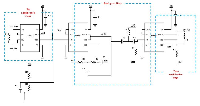
Electronics 2022, 11, x FOR PEER REVIEW 6 of 19

 Electronics 2022, 11, 1591 6 of 18

 3.2. Neural Sensor
 3.2.The
 Neural Sensor
 neural sensor circuit, called the TinyLFP, was presented in the authors’ earlier
 work [35].
 The The
 neuralcircuit
 sensor diagram is summarized
 circuit, called the TinyLFP,in was
 Figure 3. TinyLFP
 presented in theincludes the circuits
 authors’ earlier
 work [35].
 required The circuit
 to perform thediagram is summarized
 acquisition and initialinprocessing
 Figure 3. TinyLFP includes
 of the neural the circuits
 signals. It is a sin-
 required to perform the acquisition and initial processing of the neural
 gle-channel device that performs the amplification and filtering of low-amplitude signals. It is a LFP
 single-channel device that performs the amplification and filtering of low-amplitude LFP
 signals from the sensed raw neural signals. This is completed using (i) an ultra-low power
 signals from the sensed raw neural signals. This is completed using (i) an ultra-low power
 single channel precision instrumentation amplifier INA826 (3 mm × 3 mm) from Texas
 single channel precision instrumentation amplifier INA826 (3 mm × 3 mm) from Texas
 Instruments,
 Instruments,andand(ii)
 (ii)aa low-power
 low-power dual dualOpamp
 Opamp ADA4692
 ADA4692 (2 mm
 (2 mm × 2 mm)
 × 2 mm) fromfrom
 Analog Analog
 Devices,
 Devices,asaswell
 wellas
 asother
 other passive components.
 passive components.

 Figure
 Figure 3. 3. Circuitdiagram
 Circuit diagramof
 of the
 the neural
 neuralsensor.
 sensor.
 3.2.1. Pre-Amplification
 3.2.1. Pre-Amplification
 The low-noise, high-gain instrumentation amplifier INA826 forms the pre-amplification
 TheItlow-noise,
 stage. high-gain
 takes the input from theinstrumentation amplifier
 sensing and reference INA826
 electrodes, andforms
 givesthe pre-amplifica-
 a differential
 tion stage. It takes
 amplification thev/v.
 of 100 inputThefrom
 gainthe sensing
 of 100 v/v is and reference
 achieved electrodes,
 by using a resistorand of 499 aΩ,
 R1 gives differ-
 from the gain equation of INA826 given by:
 ential amplification of 100 v/v. The gain of 100 v/v is achieved by using a resistor R1 of 499
 Ω, from the gain equation of INA826 given by:
 49.4 kΩ
 Gain = 1 + . Ω
 (1)
 Gain = 1 +R (1)
 3.2.2. Filtering
 Following the initial stage of amplification, the pre-amplified signals undergo band-
 3.2.2. Filtering
 pass filtering. This is done to filter out unwanted frequencies from the raw neural signals.
 TheFollowing
 band-passthe initial
 filter has astage
 lowerof amplification,
 cut-off frequency ofthe4 Hz
 pre-amplified
 and an uppersignals
 cut-offundergo
 frequencyband-
 pass filtering.
 of 200 Hz, to This
 obtainisLFP
 done to filter
 signals out
 in the unwanted
 theta, frequencies
 alpha, beta, and gammafrom the raw
 bands. neural
 This is signals.
 realized
 The band-pass
 using filter has
 an ADA4692 dualaopamp
 lower chip.
 cut-off
 The frequency
 upper andoflower
 4 Hzcut-off
 and anfrequencies
 upper cut-off frequency
 are set by
 of using
 200 Hz,R4 to
 = R5 = 205LFP
 obtain kΩ, signals
 R6 = R7 in= 84.5
 the kΩ, C5 alpha,
 theta, = C6 = beta,
 3.9 nF,and
 andgamma
 C7 = C8 bands.
 = 0.47 µF from
 This is real-
 the cut-off frequency equation given as:
 ized using an ADA4692 dual opamp chip. The upper and lower cut-off frequencies are set
 by using R4 = R5 = 205 kΩ, R6 = R7 = 84.5 kΩ, C5 = C61= 3.9 nF, and C7 = C8 = 0.47 µF from
 the cut-off frequency equationCut − offas:
 given frequency = (2)
 2πRC
 1
 3.2.3. Post-Amplification Cut − off frequency = (2)
 2
 The pre-amplified and filtered signal is amplified further using the post-amplification
 stage, which is realized using another opamp circuit in ADA4692. The post-amplifier gives
 3.2.3. Post-Amplification
 The pre-amplified and filtered signal is amplified further using the post-amplifica-
 tion stage, which is realized using another opamp circuit in ADA4692. The post-amplifier
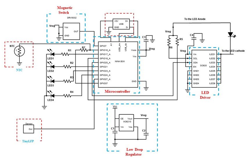
Electronics 2022, 11, x FOR PEER REVIEW 7 of 19

 Electronics 2022, 11, 1591 7 of 18
 gives an amplification of 200 v/v to the filtered LFP signals. A 200 v/v amplification is set
 using R8 = 200 Ω and R9 = 40.2 kΩ, from the amplifier gain equation given by:
 an amplification of 200 v/v to the filtered LFP signals. A 200 v/v amplification is set using

 R8 = 200 Ω and R9 = 40.2 kΩ, from the = 1 + gain equation given by:
 amplifier (3)

 R f eedback
 This helps to achieve an overall amplification of 20,000 v/v for the LFP signals in the
 Gain = 1 + (3)
 R
 range 2 Hz to 200 Hz from the raw neural input signals.
 This helps to achieve an overall amplification of 20,000 v/v for the LFP signals in the
 3.2.4.
 rangePower
 2 Hz Supply and
 to 200 Hz Virtual
 from Ground
 the raw neural input signals.
 The neural sensor is powered using a 3.3 V power source. To enable single supply
 3.2.4. Power
 operation Supply
 of the and
 neural Virtual
 sensor Ground
 circuit, and to realize a single supply analog to digital con-
 The neural
 verter (ADC), sensorground
 a virtual is powered using a 3.3
 is maintained byVmeans
 powerofsource.
 a level To enable
 shifter. single
 This supply
 is done using
 operation of the neural sensor circuit, and to realize a single supply analog
 a voltage divider circuit (R2 = R3 = 100 kΩ) followed by an opamp amplifier (ADA4692) to digital
 inconverter (ADC), configuration.
 voltage follower a virtual ground is maintained
 With 3.3 V as theby means
 supply of a level
 voltage, shifter. is
 the ground This is
 shifted
 done using a
 to about 1.65 V. voltage divider circuit (R2 = R3 = 100 kΩ) followed by an opamp amplifier
 (ADA4692) in voltage follower configuration. With 3.3 V as the supply voltage, the ground
 is shifted
 3.3. to about
 Optogenetic 1.65 V.
 Stimulator
 3.3.In closed-loop
 Optogenetic optogenetic systems, the stimulation circuit is used to control the op-
 Stimulator
 erationInofclosed-loop
 the light source, based systems,
 optogenetic on the neural signals. The
 the stimulation pulseiswidth,
 circuit used tofrequency,
 control theand
 intensity
 operationof stimulation light can
 of the light source, be modified
 based according
 on the neural to the
 signals. Theoutput
 pulseof the neural
 width, sensor.
 frequency,
 This
 andisintensity
 achievedofby sampling light
 stimulation and digitizing the amplified
 can be modified according neural
 to thesignal,
 outputrunning the clas-
 of the neural
 sification andiscontrol
 sensor. This achievedalgorithm, andand
 by sampling controlling
 digitizing the light source
 the amplified based
 neural on the
 signal, output
 running the of
 the control algorithm.
 classification Thealgorithm,
 and control circuit diagram of the stimulator
 and controlling is shown
 the light source basedinonFigure 4. The
 the output
 of the control
 stimulator algorithm.
 circuit consistsThe
 of circuit diagram of the
 a microcontroller, stimulator a
 a regulator, is voltage
 shown insupply,
 Figure 4.anThe
 LED
 stimulator
 driver, and acircuit consists
 magnetic of a microcontroller, a regulator, a voltage supply, an LED driver,
 switch.
 and a magnetic switch.

 Figure 4.4.Circuit
 Figure Circuitdiagram
 diagramof
 ofthe
 theoptogenetic stimulator.
 optogenetic stimulator.
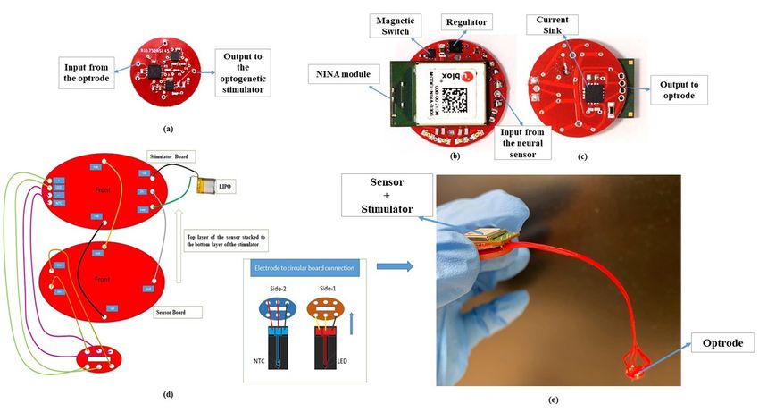
Electronics 2022, 11, 1591 8 of 18

 3.3.1. Microcontroller
 A 32-bit ARM Cortex-M4 microcontroller, nRF52840 by Nordic Semiconductors [36]
 is used as the control module in the device. The microcontroller controls the stimulation
 output, implements system logic, and facilitates programmability. A NINA B306 stand-
 alone module with an nRF52840 microcontroller is used in the circuit design, ensuring
 the ease of microcontroller programming using an USB interface. USB programming is
 achieved by using the pins USB_DP, USB_DM, and the Vbus . To enable USB programming,
 a 5 V supply input is connected to the Vbus pin. The nRF52840 has substantial memory
 availability for flash memory (1 MB) and RAM (256 kB). It has 48 general purpose I/O pins,
 12-bit 8 channel 200 ksps A/D converters, and a USB 2.0 12 Mbps controller. The NINA has
 the dimensions 11.6 mm × 10 mm × 2.23 mm, facilitating a miniaturized design including
 all the advanced features of the nRF52840 microcontroller. The microcontroller can run
 on voltages as low as 1.7 V and includes an integrated 64 MHz oscillator. A pulse width
 modulation (PWM) is used to control operation of the stimulation LED through an SC620
 current sink LED driver.

 3.3.2. Current Sink
 An SC620 by Semtech [37], with eight identical, independently controlled current
 sinks drives the µLED on the optrode for generating the stimulation light. The LED can be
 driven by connecting the anode of the LED to the power supply, and the cathode to the
 input pin of the current sink. The current sink has an adjustable current setting register,
 which allows variable current setting step sizes from 31.25 µA to 500 µA. This gives a good
 range of options for light intensity settings. An I2 C interface bus is used for programming
 the current control register. The I2 C interface involves serial clock (SCL) and serial data
 (SDA) lines, which are connected to Vcc through the pull-up resistors, R5 and R6 . The
 ultra-miniature SC620 is supplied in a 3 mm × 3 mm MLPQ-UT-16 package. It includes
 protection features such as short circuit current limit, thermal protection, and under-voltage
 lockout across all load conditions.

 3.3.3. Magnetic Switch
 Along with the above-described features, a physical interface has been created to
 enable activation and deactivation of the device, to facilitate easy user control of the board.
 A Hall effect sensor, DRV5032 from Texas Instruments, operates as a magnetic switch [38].
 Incorporating the DRV5032, the device can be turned ON and OFF manually using a
 magnet. When the applied magnetic flux density exceeds the threshold, the device outputs
 a low voltage. The output is connected to the microcontroller GPIO pin P0.25, set at input
 mode. This means that researchers need only to move a magnet within the active area of
 the sensor and the microcontroller can enable and disable the stimulation. This sensor has
 a very low power consumption of 1.6 µA at 3.3 V power supply and a tiny packaging size
 of 1.1 mm × 1.4 mm × 0.4 mm.

 3.3.4. Power Source and Regulator
 The entire clOBS device is powered by a 3.7 V 30 mAh LiPo battery. The XC6210
 low-dropout regulator (LDO) from Torex Semiconductor [39] is used to ensure low noise
 regulation of the analog supply voltages. This chip was selected because it offers low noise
 and high output current. The regulator takes 1.5–6 V and regulates it to a stable 3.3 V
 level for powering the components on the optogenetic stimulator board and the neural
 sensor board.

 3.4. Software Components
 The software component was developed using C programming language and up-
 loaded into the nRF52840 microcontroller after installing the Arduino bootloader [40]. The
 pseudocode is given in Figure 5. The firmware consists of three modules: data acquisition
 module, data processing module, and output signal generation module.
Electronics 2022, 11, x FOR PEER REVIEW 9 of 19

Electronics 2022, 11, 1591 pseudocode is given in Figure 5. The firmware consists of three modules: data acquisition
 9 of 18
 module, data processing module, and output signal generation module.

 Figure 5.
 Figure Pseudo-code for
 5. Pseudo-code for the
 the software
 software component.
 component.

 3.4.1. Data Acquisition
 3.4.1. Data Acquisition
 The data acquisition module includes code to read the pre-processed analog neural
 The data acquisition module includes code to read the pre-processed analog neural
 data from the neural sensor and the temperature monitoring circuit. The neural data is
 data from the neural sensor and the temperature monitoring circuit. The neural data is
 read using the microcontroller GPIO27_A pin. The ADC is enabled and the neural data
 read using the microcontroller GPIO27_A pin. The ADC is enabled and the neural data is
 is sampled. The neural signal is then given to a Deep Neural Network (DNN) classifier,
 sampled. The neural signal is then given to a Deep Neural Network (DNN) classifier,
 which has been described in detail in a paper by Kumari and Kouzani [41]. The classifier
 which hasneural
 takes the been described in detail
 signals, with in a paper
 a dimension ofby
 500Kumari
 samples,andandKouzani [41].them
 classifies The classifier
 into one
 takes
 of fourthe neural normal
 classes: signals,signal
 with a(class1),
 dimension of 500 samples,
 abnormal and classifies
 theta (class2), abnormal them into(class3),
 alpha one of
 four classes: normal signal (class1), abnormal theta (class2), abnormal
 or abnormal gamma (class4). Because the input dimension of the classifier is 500, the alpha (class3), or
 abnormal gamma (class4). Because the input dimension of the classifier
 sampled neural data is continuously stored in the flash memory and given to the DNN is 500, the sam-
 pled
 after neural data ishave
 500 samples continuously storedAdditionally,
 been received. in the flash memory
 the analog and given
 data from tothe
 theNTC
 DNNcircuit
 after
 500
 for temperature monitoring is sensed and sampled using the ADC on pin GPIO20_A. for
 samples have been received. Additionally, the analog data from the NTC circuit
 temperature monitoring is sensed and sampled using the ADC on pin GPIO20_A.
 3.4.2. Data Processing
 3.4.2.Data
 Dataprocessing
 Processingincludes the classification and control algorithms. During data pro-
 Datathe
 cessing, processing
 acquiredincludes the classification
 neural signals are classifiedand using
 controla algorithms.
 seven-layerDuring data pro-
 fully connected
 cessing,
 DNN-based the acquired
 classifier. neural
 The DNN signals are classified
 network is trainedusing a seven-layer
 with four fully connected
 sets of training data: nor-
 DNN-based
 mal signals, classifier. Themodified
 signals with DNN network is trained
 amplitude in thewith four
 theta bandsetsoscillations,
 of training data:
 signalsnormal
 with
 signals,
 modifiedsignals with in
 amplitude modified
 the alpha amplitude in the theta
 band oscillations, andband oscillations,
 signals signals
 with modified with mod-
 amplitude in
 the gamma band oscillations. These modified signals represent the biomarkers
 ified amplitude in the alpha band oscillations, and signals with modified amplitude in the of MDD,
 according
 gamma to the
 band literature These
 oscillations. described in Section
 modified signals1.1.represent
 Based onthe thebiomarkers
 classificationof output,
 MDD, ac- an
 On/Off control
 cording algorithmdescribed
 to the literature is used either to set 1.1.
 in Section the stimulation
 Based on the parameters (theoutput,
 classification frequency,an
 pulse width,
 On/Off and
 control duty cycle
 algorithm is of the either
 used outputtopulse)
 set theif the signal corresponds
 stimulation parametersto(theclass 2, class 3,
 frequency,
 or class
 pulse 4. The
 width, andstimulation
 duty cycle of is stopped
 the outputif pulse)
 the classification
 if the signalshows a normal
 corresponds signal.
 to class The
 2, class
 stimulation parameters are set as per Table 1, based on safe optogenetic
 3, or class 4. The stimulation is stopped if the classification shows a normal signal. Thestimulation param-
 eters [42]. Along
 stimulation with this,
 parameters are temperature
 set as per Tableis measured
 1, based on fromsafethe sampled values
 optogenetic using pa-
 stimulation the
 NTC thermistor equation, after applying a calibration. This value is
 rameters [42]. Along with this, temperature is measured from the sampled values usingthen used in the control
 the On/Off control algorithm, where the stimulation is turned off when the measured
 temperature goes above the set threshold value.
Electronics 2022, 11, 1591 10 of 18

 Table 1. Stimulation parameters for different signal classifications.

 Class Frequency TON TOFF
 Normal signal - - -
 Abnormal Theta 20 Hz 5 ms 45 ms
 Abnormal Alpha 40 Hz 5 ms 20 ms
 Abnormal Gamma 60 Hz 5 ms 11 ms

 3.4.3. Output Signal Generation
 The output signal generation module generates pulses to modulate the stimulation
 LED. The stimulation pulses for specific parameters are set in the data processing module,
 and turned on if an abnormal signal is detected. The stimulation is turned off when the
 incoming signal falls into the normal class.

 4. Physical Design
 Implementation of the clOBS device was achieved by the design and fabrication of
 printed circuit boards (PCB). Three separate boards were designed: one for the optrode,
 one for the neural sensor, and one for the optogenetic stimulator. After validation of each
 board, the boards were stacked to form the final device, as shown in Figure 6. The device
 was designed to be used as a back-mountable closed-loop optogenetic stimulation device
 for laboratory animal subjects. The boards were fabricated in a two-layer configuration.
 A description of the optrode board is given in Section 3.1. Both the neural sensor and
 optogenetic stimulator boards were designed in a circular shape and measure 8 mm in
 radius. In order to connect the optrode to the stacked device, a separate printed board in a
 circular shape was developed. The I/O pads in the optrode were connected to the pads
 Electronics 2022, 11, x FOR PEER REVIEW on
 11 of 19
 the circular board for easy connection to the device. The final back-mountable device is
 shown in Figure 6e.

 Figure6.6.Physical
 Figure Physicaldesign
 design of:
 of: (a) neural sensor board,
 board, (b)
 (b) optogenetic
 optogeneticstimulator—front,
 stimulator—front,(c)
 (c)optoge-
 optoge-
 neticstimulator—back,
 netic stimulator—back,(d)
 (d)device
 device design,
 design, and
 and (e)
 (e) final device design.

 5. Experimental Design and Results
 This section describes the experimental evaluation of the device, and the results ob-
 tained for the different components of the device including the optrode, neural sensor,
 and the optogenetic stimulator. This evaluation was carried out to validate the device
 function for the required specifications.
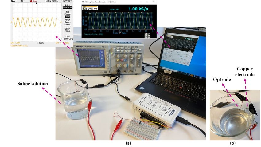
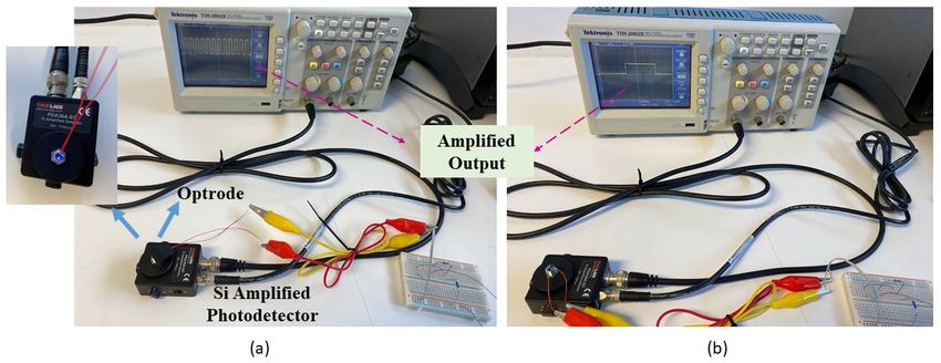
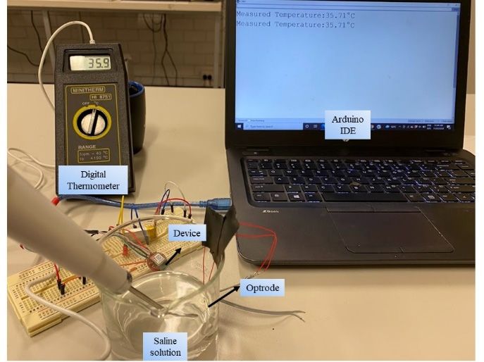
Electronics 2022, 11, 1591 11 of 18

 5. Experimental Design and Results
 This section describes the experimental evaluation of the device, and the results
 obtained for the different components of the device including the optrode, neural sensor,
 and the optogenetic stimulator. This evaluation was carried out to validate the device
 function for the required specifications.

 5.1. Optrode
 The Optrode with the µLED and NTC detection electrodes was tested to validate
 the functionality of all the components. The detection electrodes were tested using the
 experimental setup as shown in Figure 7. A sinusoidal signal of 1 V amplitude from a NI
 myDAQ was delivered to a 0.9% saline solution via a copper electrode. The saline solution
 was prepared by mixing 1.8 g of NaCl in 200 mL of distilled water, boiling the solution for
Electronics 2022, 11, x FOR PEER REVIEW15 min, and then returning it to room temperature [35]. The detection electrodes12 of 19
 were able
 to detect the signals, as can be seen on the oscilloscope in Figure 7.

 Figure
 Figure 7. Experimental
 7. Experimental evaluation
 evaluation ofofthe
 thedetection
 detectionelectrode
 electrode of the
 the optrode,
 optrode,(a)(a)the experimental
 the experimental setup
 setup
 withwith
 1 V1V sinusoidal
 sinusoidal signal
 signal delivered
 delivered to the
 to the saline
 saline solution
 solution using
 using a NI amyDAQ,
 NI myDAQ, andsignal
 and the the signal
 detected
 detected
 at the at the detection
 detection electrode
 electrode shown shown on the oscilloscope,
 on the oscilloscope, andsaline
 and (b) the (b) the saline setup
 solution solution setup the
 showing
 showing the copper electrode to deliver the signal, and the optrode to
 copper electrode to deliver the signal, and the optrode to detect the signal. detect the signal.

 Optical analysis
 Optical analysisof of
 thethe
 light source
 light sourceininthe
 theoptrode
 optrodewas
 wasundertaken
 undertaken using
 using an amplified,
 ampli-
 fied, switchable-gain,silicon
 switchable-gain, siliconphotodetector,
 photodetector,PDA36A-EC
 PDA36A-EC by by Thorlabs asas shown
 shownin inFigure
 Figure 8.
 8. This was done to verify the linear relationship between the stimulating
 This was done to verify the linear relationship between the stimulating pulses and pulses and thethe
 light coming
 light outout
 coming of the µLED.
 of the µLED. TheThe
 µLED
 µLEDwaswastested by by
 tested mounting thethe
 mounting light source
 light on on
 source thethe
 input aperture
 input of the
 aperture photodetector.
 of the photodetector. TheThe
 µLEDµLED on on
 thethe
 optrode waswas
 optrode controlled by by
 controlled pulses
 pulses
 generated using
 generated anan
 using Arduino
 Arduino mega
 mega2560
 2560board
 boardwith
 withpulse
 pulsewidths
 widths of 1 ms,
 ms, 10
 10ms,
 ms,100
 100ms
 msand
 and1000
 1000ms.
 ms.The
 Theoutput
 outputof ofthe
 thephotodetector
 photodetector was was displayed on the oscilloscope,
 oscilloscope, illustrat-
 illustrating
 ingthe
 thelinear
 linearrelationship.
 relationship.
 The temperature monitoring feature was validated using the experimental setup as
 shown in Figure 9. The optrode with the NTC sensor (ERTJZET202J) attached to its tip
 was placed on a saline solution. The temperature detected using the sensor was displayed
 on the serial monitor of the Arduino IDE. The temperature of the saline solution was also
 monitored using a Minitherm HI 8751 digital thermometer by Hanna Instruments [43].
 Table 2 gives the temperature measurements of the saline solution using the clOBS device
 and the digital thermometer.

 Figure 8. Experimental design for the optical evaluation of the optrode, with the oscilloscope show-
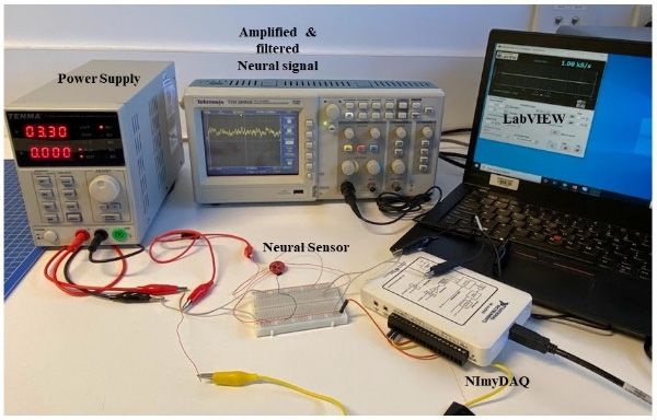
fied, switchable-gain, silicon photodetector, PDA36A-EC by Thorlabs as shown in Figure
 8. This was done to verify the linear relationship between the stimulating pulses and the
 light coming out of the µLED. The µLED was tested by mounting the light source on the
 input aperture of the photodetector. The µLED on the optrode was controlled by pulses
 generated using an Arduino mega 2560 board with pulse widths of 1 ms, 10 ms, 100 ms
Electronics 2022, 11, 1591 12 of 18
 and 1000 ms. The output of the photodetector was displayed on the oscilloscope, illustrat-
 ing the linear relationship.

 Figure 8. Experimental design
 design for
 for the
 theoptical
 opticalevaluation
 evaluationofofthe
 theoptrode,
 optrode,with
 withthe oscilloscope
 the showing
 oscilloscope show-
Electronics 2022, 11, x FOR PEER REVIEW 13 of 19
 ing the output
 the output corresponding
 corresponding to: (a)to: (a) stimulation
 stimulation pulse width
 pulse width of and
 of 10 ms, 10 ms,
 (b) and (b) stimulation
 stimulation pulse
 pulse width of
 width of 1000 ms.
 1000 ms.

 The temperature monitoring feature was validated using the experimental setup as
 shown in Figure 9. The optrode with the NTC sensor (ERTJZET202J) attached to its tip
 was placed on a saline solution. The temperature detected using the sensor was displayed
 on the serial monitor of the Arduino IDE. The temperature of the saline solution was also
 monitored using a Minitherm HI 8751 digital thermometer by Hanna Instruments [43].
 Table 2 gives the temperature measurements of the saline solution using the clOBS device
 and the digital thermometer.

 Figure
 Figure 9.
 9. Experimental
 Experimentaldesign
 designto
 to validate
 validate the
 the temperature
 temperature monitoring
 monitoring aspect
 aspect of
 of the
 the device.
 device.

 Table 2.
 Table Comparison between
 2. Comparison between the
 thetemperatures
 temperatures measured
 measured using
 using aa digital
 digital thermometer
 thermometer and
 and the
 theNTC
 NTC
 sensor
 sensor in
 in saline
 saline solution.
 solution.

 Temperature
 Temperatureof
 ofthe
 the Saline Solution
 Saline Solution Measured
 MeasuredTemperature
 Temperature
 39.8
 39.8 39.69
 39.69
 38.5
 38.5 38.34
 38.34
 36.6
 36.6 36.35
 36.35
 35.2
 35.2 34.98
 34.98
 34.6 34.39
 34.6 34.39
 5.2. Neural Sensor
 5.2. Neural Sensor
 The neural sensor was tested using raw neural signals and sinusoidal signals to
 The neural sensor was tested using raw neural signals and sinusoidal signals to val-
 validate the amplification and filtering specifications. Figure 10 shows the experimental
 idate the amplification and filtering specifications. Figure 10 shows the experimental set-
 set- p raw neural signals obtained from Razaei et al. [44]. The neural signals were from
 p raw neural signals obtained from Razaei et.al. [44]. The neural signals were from the
 the mouse hippocampus. The signal in the micro voltage was amplified by 20,000 v/v.
 mouse hippocampus. The signal in the micro voltage was amplified by 20,000 V/V. The
 The amplification factor was verified using sinusoidal signals generated using a National
 amplification factor
 Instruments (NI) was verified
 myDAQ, using in
 as shown sinusoidal
 Figure 11.signals generated using
 1 V peak-peak a National
 sinusoidal signalIn-
 of
 struments
 frequency 38(NI)
 HzmyDAQ, as shown
 was generated usinginthe
 Figure 11. generator
 function 1 V peak-peak sinusoidal
 functionality signal
 of the of fre-
 NI myDAQ.
 quency 38 Hz
 The signal was
 was generated
 further usingtothe
 reduced 100function generator
 µV using functionality
 a voltage of the NI
 divider circuit to myDAQ.
 make the
 The signal was further reduced to 100 µV using a voltage divider circuit to make
 amplitude similar to neural signals. The output as shown in Figure 11a was approximately the am-
 plitude similar to neural signals. The output as shown in Figure 11a was approximately
 equal to 2 V, which validates an amplification factor of 20,000. The filtering property was
 equal to 2V,
 validated bywhich validates
 providing an amplification
 sinusoidal factor of 20,000.
 signal of frequency 1 KHz.The
 Thefiltering
 output,property
 as shown wasin
 validated by providing sinusoidal signal of frequency 1 KHz. The output, as shown
 Figure 11b shows that the signal outside the passband of 4 Hz to 200 Hz was filtered out by in
 Figure 11b shows that the signal outside the passband of 4 Hz to 200 Hz was filtered out
 the device.
 by the device.
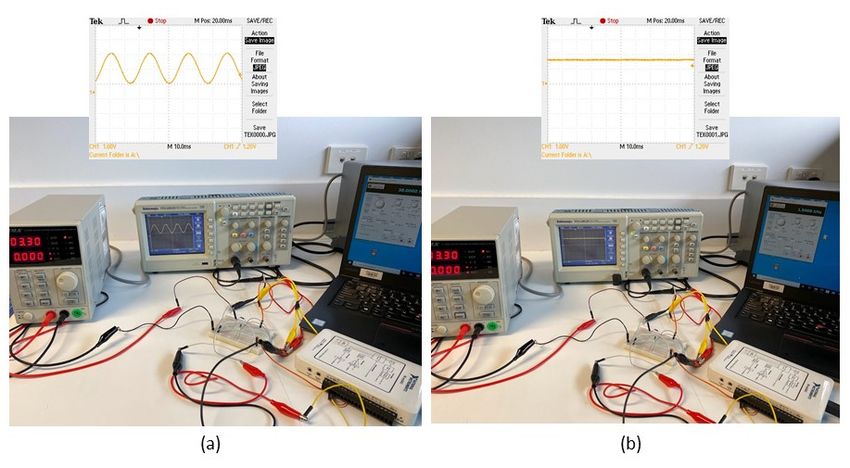
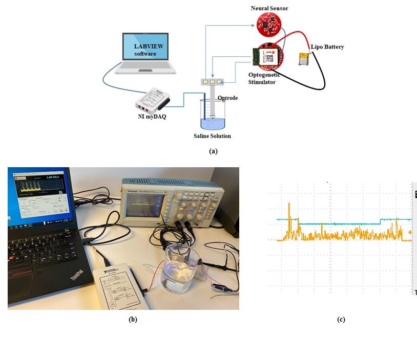
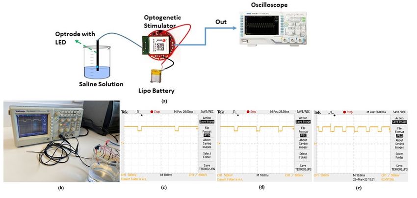
Electronics 2022, 11, x FOR PEER REVIEW 14 of 19
Electronics 2022, 11, x FOR PEER REVIEW 14 of 19
 Electronics 2022, 11, 1591 13 of 18

 Figure
 Figure 10. Experimental
 Experimentaldesign
 designforfor
 thethe neural
 neural sensor
 sensor withwith pre-recorded
 pre-recorded neuralneural signals.
 signals.
 Figure10.
 10. Experimental design for the neural sensor with pre-recorded neural signals.

 Figure 11. Experimental design for the neural sensor with: (a) sinusiodal signal of frequency 38 Hz,
 Figure 11. Experimental design for the neural sensor with: (a) sinusiodal signal of frequency 38 Hz,
 Figure
 and (b) 11. Experimental
 sinusoidal signal ofdesign
 1 kHz. for the neural sensor with: (a) sinusiodal signal of frequency 38 Hz,
 and (b) sinusoidal signal of 1kHz.
 and (b) sinusoidal signal of 1kHz.
 5.3. Optogenetic Stimulation Device
 5.3. Optogenetic Stimulation
 In vitro testing Device stimulation device was performed using the experi-
 of the optogenetic
 5.3. Optogenetic Stimulation Device
 mentalIn setup
 vitro testing
 as shown ofin
 the optogenetic
 Figure stimulationstimulator
 12. The optogenetic device was to performed using the exper-
 control the stimulation
 In vitro testing of the optogenetic stimulation device was performed using the exper-
 µLED in the optrode was powered using a 3.7 V LiPo battery. Saline
 imental setup as shown in Figure 12. The optogenetic stimulator to control the solution was prepared
 stimulation
 imental
 as described
 setup as shown in Figure 12. The optogenetic stimulator to control the stimulation
 µLED in theinoptrode
 Section 5.1.
 wasThe optrode using
 powered was placed
 a 3.7inVthe saline
 LiPo solution
 battery. and the
 Saline generated
 solution was pre-
 µLED verified
 pulses in the optrode
 for each was
 class. powered
 Figure using
 12c,d,f a 3.7the
 shows V LiPo battery.
 generated Saline solution
 stimulation pulses was pre-
 with
 pared as described in Section 5.1. The optrode was placed in the saline solution and the
 different pulse widths set as per Table 1. Thus, an in vivo open loop operation of theand the
 pared as described in Section 5.1. The optrode was placed in the saline solution
 generated pulses verified for each class. Figure 12c,d,f shows the generated stimulation
 generated pulses
 optogenetic verified
 stimulation forwas
 device each class. Figure
 evaluated through 12c,d,f shows the generated stimulation
 this experiment.
 pulses with different pulse widths set as per Table 1. Thus, an in vivo open loop operation
 pulses with different pulse widths set as per Table 1. Thus, an in vivo open loop operation
 of the
 5.4. In optogenetic
 Vitro stimulation
 Validation of the Devicedevice was evaluated through this experiment.
 of the optogenetic stimulation device was evaluated through this experiment.
 Following the bench testing of various components, in vitro testing of the optogenetic
 stimulation device was performed using the experimental setup shown in Figure 12. Raw
 neural signals obtained from Razaei et al. [40] were modified to account for the electrophysi-
 ological biomarkers of MDD, i.e., amplitude changes in theta band, alpha band, and gamma
 band oscillations. This was performed in Matlab, using Fourier transform to convert the
 time domain signals into the frequency domain. This was followed by application of filters
Electronics 2022, 11, 1591 14 of 18

 to separate the signals into theta, alpha, and gamma band oscillations. These signals were
 then modified in amplitude and converted back to the time domain using inverse Fourier
 transformation. These signals were previously used for training and testing the DNN
 classifier [34]. As shown in Figure 13a, the amplitude modified signals were sent to the
 neural sensor through an NI myDAQ, and the amplified output of the device given to the
 optogenetic stimulator for signal classification, modulating the stimulation light output.
 Electronics 2022, 11, x FOR PEER REVIEW 15 of 19
 Figure 13c shows the output of the neural sensor in yellow and the stimulation pulses in
 blue, as seen on an oscilloscope.

 Figure 12.(a)
 Figure12.
Electronics 2022, 11, x FOR PEER REVIEW (a)Experimental
 Experimentaldesign
 designfor
 forthe
 theoptogenetic
 optogeneticstimulator, (b)(b)
 stimulator, experimental setup
 experimental forfor
 setup valida-
 16 ofvali-
 19
 tion of the
 dation optogenetic
 of the stimulator,
 optogenetic (c) stimulation
 stimulator, pulsespulses
 (c) stimulation for class
 for2,class
 (d) stimulation pulses for
 2, (d) stimulation classfor
 pulses 3,
 class(e)
 and 3,stimulation
 and (e) stimulation pulses
 pulses for class for
 4. class 4.

 5.4. In Vitro Validation of the Device
 Following the bench testing of various components, in vitro testing of the optogenetic
 stimulation device was performed using the experimental setup shown in Figure 12. Raw
 neural signals obtained from Razaei et.al. [40] were modified to account for the electro-
 physiological biomarkers of MDD, i.e., amplitude changes in theta band, alpha band, and
 gamma band oscillations. This was performed in Matlab, using Fourier transform to con-
 vert the time domain signals into the frequency domain. This was followed by application
 of filters to separate the signals into theta, alpha, and gamma band oscillations. These sig-
 nals were then modified in amplitude and converted back to the time domain using in-
 verse Fourier transformation. These signals were previously used for training and testing
 the DNN classifier [34]. As shown in Figure 13a, the amplitude modified signals were sent
 to the neural sensor through an NI myDAQ, and the amplified output of the device given
 to the optogenetic stimulator for signal classification, modulating the stimulation light
 output. Figure 13c shows the output of the neural sensor in yellow and the stimulation
 pulses in blue, as seen on an oscilloscope.

 Figure 13. Experimental design for the neural sensor with: (a) sinusiodal signal of frequency 38 Hz
 Figure
 and (b)13.sinusoidal
 Experimental design
 signal for the
 of 1 kHz (c) neural
 outputsensor
 of the with:
 neural(a)sensor
 sinusiodal signal and
 (in yellow) of frequency 38 Hz
 the stimulation
 and (b) sinusoidal signal of 1 kHz (c) output of the neural sensor (in yellow) and the stimulation
 pulses (in blue) on an oscilloscope.
 pulses (in blue) on an oscilloscope.

 6. Discussion
 This paper presents a miniaturized closed-loop optogenetic brain stimulation device
 to be used for small laboratory animal subjects in the study of MDD. The device has the
 ability to classify incoming raw neural signals into normal, abnormal theta, abnormal al-
Electronics 2022, 11, 1591 15 of 18

 6. Discussion
 This paper presents a miniaturized closed-loop optogenetic brain stimulation device
 to be used for small laboratory animal subjects in the study of MDD. The device has the
 ability to classify incoming raw neural signals into normal, abnormal theta, abnormal alpha,
 and abnormal gamma signals. After classification, the device modifies the stimulation
 parameters based on the signal classification. For this, the device uses miniaturized circuits
 incorporating analog signal amplification and filtering, driving µLED, and on-board soft-
 ware processes including signal classification and control signal generation. The device
 is operated using a 3.7 V LiPo battery. Thus, the device benefits from circuit miniaturiza-
 tion and portability. Training and testing of the DNN model and validation of the device
 were completed using modified raw neural signals obtained from the hippocampus of a
 laboratory animal model [37].
 The evaluation of the device was carried out using bench testing and in vitro experi-
 ments, using saline solution to replicate the brain environment. Bench testing of different
 components of the device, including the neural sensor, stimulator, and optrode were con-
 ducted to verify successful operation according to the specifications. After bench testing
 the individual components, in vitro testing of the device was conducted in both open-loop
 and closed-loop configurations.
 Table 3 compares features of the different components of this device with existing
 clOBS devices. These other clOBS devices were reported by Turcotte et al. [20], Liu et al. [45],
 Ramezani et al. [46,47] and Mendrela et al. [48]. While most of these devices are tetherless,
 the current work is the first device to use on-device processing of neural signals using an
 AI-based algorithm, along with miniaturization and tetherless operation.

 Table 3. Comparison of the component features of the presented device with existing clOBS devices.

 [20] [45] [46,47] [48]
 References This Work
 (2019) (2018) (2020) (2018)
 Portability Tetherless Tetherless Tetherless Tethered Tetherless
 Biomarker LFP, AP LFP LFP LFP, AP LFP
 No: of recording
 10 16 4 32 1
 channels
 Recording circuit ASIC COTS ASIC COTS COTS
 Gain NG NG 49.54 dB NG 85 dB
 Bandwidth 0.1–7 kHz NG 9.8 µW/Channel NG 4 Hz–200 Hz
 Adaptive
 AI based
 thresholding, Amplitude threshold, Spike sorting,
 Algorithm Amplitude threshold classification,
 wavelet ON/OFF control thresholding
 ON/OFF control
 compression
 ASIC +
 Platform MCU ASIC + MCU PC MCU
 FPGA
 On-device
 Data transmission Wireless - SPI protocol USB interface
 processing
 Light source LED µLED µLED µLED µLED
 Stimulating circuit ASIC COTS ASIC ASIC COTS
 No: of channels 4 - 6 12 1
 Power supply Battery Battery Battery Battery Battery
 10 mm × 10 mm
 21.2 mm × 31.8 mm (headstage) 2.16 cm × 2.38 cm
 Dimension 1.61 cm × 1.16 cm 8 mm (headstage)
 × 1 mm (board) 25 mm × 22 mm × 0.35 cm
 (control unit)

 With advances in device engineering and signal processing technologies, miniatur-
 ization, portability, and progression in functionalities of closed-loop optogenetic brain
 stimulation devices have been achieved. The presented clOBS device is a step towards ad-
Electronics 2022, 11, 1591 16 of 18

 vancement of miniature devices capable of noise-free sensing of very low amplitude neural
 signals in low frequency bands, and closed-loop optogenetic stimulation after signal classi-
 fication using a DNN classifier on-board a resource constraint microcontroller. An accuracy
 of around 75% was obtained during the testing of the DNN classifier [34]. Because the
 sensed neural signals are time-series signals, recurrent neural networks such as long short-
 term memory (LSTM) networks [49] could be a more efficient classifier. However, it may not
 be practical to deploy such a resource-intensive network on a 256 kB RAM microcontroller.
 Further improvement in controller design for tiny devices might involve deploying more
 efficient algorithms using technologies such as tinyML [22]. Other additions to the design
 could involve implementation of phase-specific stimulation [50]. As the device senses
 neural oscillations in the LFP band, sending timely stimulation pulses in phase with the
 incoming neural signals could increase the accuracy of the brain stimulation paradigm.

 7. Conclusions
 There is a need for further research in hardware and software engineering features
 of closed-loop optogenetic brain stimulation, to enable efficient utilization of the relevant
 technology. With researchers now adopting optogenetic brain stimulation techniques for
 comprehending different neurological disorders in laboratory animal models, effective
 stimulation devices are required to support the research. To address this necessity, the
 presented device is miniaturized and light-weight. Moreover, the device is tetherless and
 has very low-power operation suitable for laboratory animal models of diseases. The ap-
 proach is also a step towards the use of on-device AI in brain stimulation devices. However,
 there is scope for improvement in the design, including the control algorithm, selection of
 biomarkers, and hardware deployment of the classification algorithm. Additionally, a clear
 next step in the device’s development will be to perform in vivo brain stimulation using
 the presented device, for direct evaluation of its closed-loop operation using biomarkers
 directly obtained from the animal model of the disease.

 Author Contributions: Conceptualization, L.S.K. and A.Z.K.; methodology, L.S.K. and A.Z.K.; soft-
 ware, L.S.K. and A.Z.K.; validation, L.S.K.; formal analysis, L.S.K.; investigation, L.S.K.; resources,
 A.Z.K.; data curation, L.S.K.; writing—original draft preparation, L.S.K.; writing—review and edit-
 ing, L.S.K. and A.Z.K.; visualization, L.S.K.; supervision, A.Z.K.; project administration, A.Z.K. All
 authors have read and agreed to the published version of the manuscript.
 Funding: This research received no external funding.
 Conflicts of Interest: The authors declare no conflict of interest.

References
1. Cash, R.F.; Cocchi, L.; Lv, J.; Fitzgerald, P.B.; Zalesky, A. Functional magnetic resonance imaging–guided personalization of
 transcranial magnetic stimulation treatment for depression. JAMA Psychiatry 2021, 78, 337–339. [CrossRef] [PubMed]
2. Beliaeva, V.; Savvateev, I.; Zerbi, V.; Polania, R. Toward integrative approaches to study the causal role of neural oscillations via
 transcranial electrical stimulation. Nat. Commun. 2021, 12, 1–12. [CrossRef] [PubMed]
3. Sudbrack-Oliveira, P.; Barbosa, M.Z.; Thome-Souza, S.; Razza, L.B.; Gallucci-Neto, J.; Valiengo, L.d.C.L.; Brunoni, A.R. Transcranial
 direct current stimulation (tDCS) in the management of epilepsy: A systematic review. Seizure 2021, 86, 85–95. [CrossRef]
 [PubMed]
4. Elyamany, O.; Leicht, G.; Herrmann, C.S.; Mulert, C. Transcranial alternating current stimulation (tACS): From basic mechanisms
 towards first applications in psychiatry. Eur. Arch. Psychiatry Clin. Neurosci. 2021, 271, 135–156. [CrossRef] [PubMed]
5. Spix, T.A.; Nanivadekar, S.; Toong, N.; Kaplow, I.M.; Isett, B.R.; Goksen, Y.; Pfenning, A.R.; Gittis, A.H. Population-specific
 neuromodulation prolongs therapeutic benefits of deep brain stimulation. Science 2021, 374, 201–206. [CrossRef] [PubMed]
6. Christenson Wick, Z.; Krook-Magnuson, E. Specificity, versatility, and continual development: The power of optogenetics for
 epilepsy research. Front. Cell. Neurosci. 2018, 12, 151. [CrossRef]
7. Fougère, M.; van der Zouwen, C.I.; Boutin, J.; Neszvecsko, K.; Sarret, P.; Ryczko, D. Optogenetic stimulation of glutamatergic
 neurons in the cuneiform nucleus controls locomotion in a mouse model of Parkinson’s disease. Proc. Natl. Acad. Sci. USA 2021,
 118, 43. [CrossRef]
8. Shimoda, Y.; Beppu, K.; Ikoma, Y.; Morizawa, Y.M.; Zuguchi, S.; Hino, U.; Yano, R.; Sugiura, Y.; Moritoh, S.; Fukazawa, Y.
 Optogenetic stimulus-triggered acquisition of seizure resistance. Neurobiol. Dis. 2021, 163, 105602. [CrossRef]
You can also read