An Integrated 2D Ultrasound Phased Array Transmitter in CMOS with Pixel Pitch-Matched Beamforming
←
→
Page content transcription
If your browser does not render page correctly, please read the page content below
This article has been accepted for publication in a future issue of this journal, but has not been fully edited. Content may change prior to final publication. Citation information: DOI 10.1109/TBCAS.2021.3096722, IEEE
Transactions on Biomedical Circuits and Systems
> REPLACE THIS LINE WITH YOUR PAPER IDENTIFICATION NUMBER (DOUBLE-CLICK HERE TO EDIT) < 1
An Integrated 2D Ultrasound Phased Array
Transmitter in CMOS with Pixel Pitch-
Matched Beamforming
Tiago Costa, Member, IEEE, Chen Shi, Kevin Tien, Jeffrey Elloian, Filipe A. Cardoso and Kenneth L.
Shepard, Fellow, IEEE
Abstract— Emerging non-imaging ultrasound
applications, such as ultrasonic wireless power delivery to
implantable devices and ultrasound neuromodulation,
require wearable form factors, millisecond-range pulse
durations and focal spot diameters approaching 100 µm
with electronic control of its three-dimensional location.
None of these are compatible with typical handheld linear
array ultrasound imaging probes. In this work, we present
a 4 mm x 5 mm 2D ultrasound phased array transmitter
with integrated piezoelectric ultrasound transducers on
complementary metal-oxide-semiconductor (CMOS)
integrated circuits, featuring pixel-level pitch-matched
transmit beamforming circuits which support arbitrary
pulse duration. Our direct integration method enabled up Fig. 1. Conceptual application of a wearable device performing ultrasound
neuromodulation of a peripheral neve and powering implantable devices, with
to 10 MHz ultrasound arrays in a patch form-factor, 3D control of focal sot location.
leading to focal spot diameter of ~200 µm, while pixel pitch-
matched beamforming allowed for precise three-
when comparing to traditional ultrasound imaging applications.
dimensional positioning of the ultrasound focal spot. Our
device has the potential to provide a high-spatial resolution While in imaging short bursts of focused pulsed waves
and wearable interface to both powering of highly- sequentially generated by subsections of a one-dimensional
miniaturized implantable devices and ultrasound array can produce high-quality two-dimensional images, in
neuromodulation. both ultrasound neuromodulation and power delivery, long
bursts of pulsed waves generated by all acoustic sources of a
Index Terms—2D ultrasound phased-array, PZT integration, two-dimensional array with three-dimensional control of focal
piezoelectric ultrasound transducers, phased-array beamforming, spot are required to achieve high spatial resolution and power
ultrasound neuromodulation, ultrasound powered implantable efficiency [5, 11]. In addition, these applications would benefit
devices. significantly from wearable ultrasound phased-array form-
factors, which are still far from the commercially available
hand-held ultrasound phased-array probes. Such a form factor
I. INTRODUCTION
requires single-chip integration of the electronics for the device
L EVERAGING decades of technological advances in the
field of ultrasound medical diagnostic imaging, new
ultrasound biomedical applications are now emerging, such as
as well as the integration of transducer elements. This direct
integration allows arrays to be sized to almost arbitrary scale
and aspect ratios because of local interconnection between
ultrasound neuromodulation [1-6] and ultrasonic power front-end electronics and transducer. It also allows ultrasound
delivery and communication for medical implants [7-14]. These frequencies to be scaled higher towards smaller focal spots,
applications benefit from the attractive properties of ultrasound both in supporting the tighter pitch required for transducer
energy propagation and interaction with tissue, such as low elements in this case and in reducing electrical parasitics
scattering, low attenuation, and safe energy levels. between the transducer and the front-end electronics which
Furthermore, they require different ultrasound wave parameters
T. Costa was the Bioelectronic Systems Lab, Department of Electrical C. Shi, K. Tien, J. Elloian, F. A. Cardoso, and K. L. Shepard are with the
Engineering, Columbia University, New York, NY 10027 USA. He is now with Bioelectronic Systems Lab, Department of Electrical Engineering, Columbia
the Department of Microelectronics, Delft University of Technology, 2628 CD University, New York, NY 10027 USA (e-mail: cs3184@columbia.edu;
Delft, The Netherlands (e-mail: t.m.l.dacosta@tudelft.nl). ktien@ee.columbia.edu; jelloian@ee.columbia.edu; fa2495@columbia.edu,
shepard@ee.columbia.edu)
1932-4545 (c) 2021 IEEE. Personal use is permitted, but republication/redistribution requires IEEE permission. See http://www.ieee.org/publications_standards/publications/rights/index.html for more information.
Authorized licensed use limited to: Columbia University Libraries. Downloaded on July 16,2021 at 19:59:11 UTC from IEEE Xplore. Restrictions apply.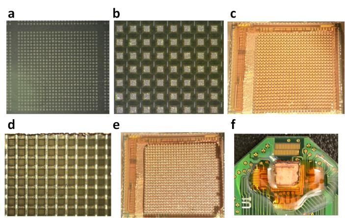
This article has been accepted for publication in a future issue of this journal, but has not been fully edited. Content may change prior to final publication. Citation information: DOI 10.1109/TBCAS.2021.3096722, IEEE
                                                                                        Transactions on Biomedical Circuits and Systems
          > REPLACE THIS LINE WITH YOUR PAPER IDENTIFICATION NUMBER (DOUBLE-CLICK HERE TO EDIT) <                                                                                                            2

          more significantly limit performance as the frequency is scaled.
          Smaller focal spots allow for more efficient powering of
          distributed sub-mm implantable devices, and also for higher-
          precision non-invasive neuromodulation of peripheral nerves.
          For neuromodulation applications in the brain, chip form-
          factors could also enable placement below the skull to allow for
          stimulating cortical circuits with high precision. This would
          alleviate the hurdles faced in transcranial ultrasound
          stimulation, where frequencies below 1 MHz are typically used
          to overcome the large acoustic attenuation in the skull, which
          reduces spatial resolution.
             In the absence of commercially available phased-array                                              Fig. 2. 2D ultrasound phased array transmitter: properties of transducer driving
          technology matching the abovementioned requirements,                                                  signals, transducer array and focused ultrasound waves.
          researchers have been using commercially available single                                            full array aperture. These properties enable the individual
          element focused transducers for these new non-imaging                                                configuration of the delay of each ultrasound transmitter with
          applications [1, 5, 11]. However, in addition to the very large                                      arbitrary pulse duration (PD), allowing for high-spatial-
          size of these transducers, changing the focal spot location                                          resolution volumetric control of the ultrasound focal spot in
          requires physically moving the transducer, necessitating the use                                     three dimensions.
          of precise micro-manipulators, and, as a consequence, a more                                            This article expands on our previous reporting on this design
          complex and bulky setup. These limitations of existing                                               [25] by providing an in-depth system level analysis, a
          transducers are a major limiting factor in the advancement of                                        comprehensive PZT integration description and a detailed
          emerging applications of ultrasound. The work presented here                                         analysis of the experimental characterization. The organization
          builds on prior efforts to develop miniaturized transducers with                                     of this article is as follows: Section II presents the system design
          different form factors, such as disks [15], needles [16], flexible                                   of our approach. Section III analysis the choice of the
          arrays [17-19] and IC 2D phased arrays [20-24]. However,                                             ultrasound transducer material. Section IV discusses the circuit
          unlike our proposed device, most of these systems do not allow                                       level design of the CMOS IC. Section V presents the
          electronic beam-steering for control of focal spot location [15,                                     experimental electrical characterization of the CMOS IC.
          16], still have large form factors [17] or are completely passive                                    Section VI introduces our method to integrate PZT transducers
          relying on extensive external electronics [18, 19]. IC 2D                                            on top of CMOS ICs. Section VII presents the ultrasound
          phased arrays, on the other hand, have been mostly designed for                                      characterization results, and Section VIII concludes the paper.
          ultrasound imaging applications, by supporting only pulsed-
          wave operation [20-23] and having small transmitter apertures                                                                         II. SYSTEM DESIGN
          [21] in exchange for large receiving apertures towards high
          image quality. A 2D phased array with full transmitter aperture                                         To be compatible with the requirements for ultrasound
          for brain stimulation has been recently proposed [24], however,                                      neuromodulation and ultrasound powered implantable devices
          ultrasound frequency is still limited to 2 MHz, which leads to                                       (Fig. 1), the interfacing IC needs to allow for precise phase
          focal spot dimensions in the millimeter range, still large in                                        control of the driving signals of each transducer while allowing
          comparison with the scales of sub-mm ultrasound powered                                              arbitrary PD. In contrast to ultrasound imaging applications,
          implantable devices and neuronal circuits.                                                           where pulsed waves must be generated, in this application,
             In this article, we describe a 10 MHz 26 × 26 two-                                                continuous-wave signals are desirable, both for allowing higher
          dimensional (2D) phased array ultrasound transmitter in a                                            available power in ultrasound powered implantable devices [7,
          single-chip form-factor [25] in line with the “more-than-                                            9-11], and for meeting the PD specifications of ultrasound
          Moore” paradigm [26]. The transmitter is implemented as an                                           neuromodulation [1]. In such a continuous-wave mode, an
          integrated device with a 2D array of lead zirconate titanate                                         arbitrary PD is easily achieved with a single enable input signal,
          (PZT) piezoelectric transducers directly microfabricated on top                                      rather than the more complex counter-based approaches
          of a complementary metal-oxide-semiconductor (CMOS)                                                  required in pulsed-mode ultrasound [20]. In addition, these
          integrated circuit (IC). PZT exhibits higher transmit                                                applications also demand a higher spatial resolution for the
          electroacoustic sensitivity (Stx) than capacitive and piezoelectric                                  ultrasound focal spot, which can be achieved by increasing the
          micromachined ultrasound transducers (CMUT, PMUT,                                                    ultrasound frequency. Here, continuous-wave beamforming
          respectively) [27, 28], which is critical for the applications                                       can potentially lead to a design with a reduced area to
          targeted in this work. This direct integration leads to several                                      accommodate the tighter pitch between the transducers, by
          orders of magnitude smaller form-factors when compared to                                            exploring the periodicity of continuous ultrasound waves (Fig.
          commercially available transducers and a decrease of the                                             2). Finally, to maximize power delivery to implantable devices,
          parasitic capacitance for interconnection between transducer                                         and ensure successful neuromodulation, focal pressure should
          and transmitter circuits to only a few fF. This allowed the device                                   be maximized.
          to generate 10 MHz focused ultrasound waves with a pixel-                                               In Fig. 2, the relevant characteristics of focused ultrasound
          level pitch-matched array of transmitter circuits occupying the

  1932-4545 (c) 2021 IEEE. Personal use is permitted, but republication/redistribution requires IEEE permission. See http://www.ieee.org/publications_standards/publications/rights/index.html for more information.
                    Authorized licensed use limited to: Columbia University Libraries. Downloaded on July 16,2021 at 19:59:11 UTC from IEEE Xplore. Restrictions apply.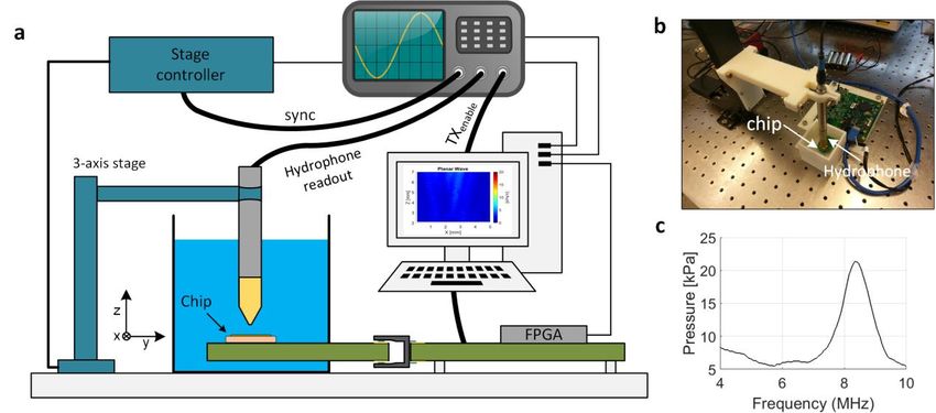
This article has been accepted for publication in a future issue of this journal, but has not been fully edited. Content may change prior to final publication. Citation information: DOI 10.1109/TBCAS.2021.3096722, IEEE
Transactions on Biomedical Circuits and Systems
> REPLACE THIS LINE WITH YOUR PAPER IDENTIFICATION NUMBER (DOUBLE-CLICK HERE TO EDIT) < 3
waves, transducer geometry and driving signals are depicted. A
CMOS ultrasound transmitter is programmed to generate
driving signals with a given frequency (fUS), PD, and a delay
with a given timing resolution (Tmin). Each signal is applied to
a piezoelectric transducer within a 2D array organization with
an aperture L and an inter-element pitch d. With carefully
defined delays for 2D beamforming [29], the piezoelectric
transducers generate focused ultrasound waves at a pre-
determined depth (Zm, up to a maximum Zt) and steering angle,
in both the XZ (θXZ) and YZ planes (θYZ). The focal spot
properties are characterized by the full width at half maximum
(FHWM), the depth of field (DOF) and the focusing gain
(Gain). The interplay between the abovementioned
characteristics must be understood. The main design variables
influencing the focal spot characteristics are the wavelength of
the ultrasound waves (λ) and L. λ is readily derived from fUS and
the speed of sound in soft tissue (~1540 m/s). L, on the other
hand, is given by:
Ld N 1 (1)
Where N is the number of transducers of a squared 2D phased
array. To avoid grating lobes in the field of view of the
transducer array, d must respect the condition given by (2),
where θmax is the maximum of θXZ and θYZ [30]. For θmax of ±90°,
Fig. 3. Focusing properties of integrated 2D ultrasound phased arrays. a,b,
d has a minimum value at λ/2. simulated beam profiles of an ultrasound wave with N of 5 mm generated by a
(2) 16x16 2D ultrasound array (a) and 32x32 2D ultrasound array (b). c,d,e,f,
d
1 sin max influence of array aperture on FWHM (c), DOF (d), Gain (e) and Zm (f).
devices featuring ultrasound power delivery and data telemetry
The focal spot properties FHWM, DOF, Zt and Gain relate to λ have recently evolved into the sub-mm scale, with sizes as small
and L as shown in (4), (5), (6), and (7), respectively. as 380 μm × 300 μm × 570 μm [13]. On the other hand, in the
Zm (3) micrometer scales of neuronal circuits both in the CNS and PNS
FWHM demand matching spatial resolution from neuromodulation
L
devices. For these reason, λ was set to 150 µm, which in soft
Zm2 tissue translates into an fUS of 10 MHz.
DOF (4)
L2 To properly dimension the optimal L, its influence on the
focal spot dimensions properties was evaluated through k-wave
L2 [32] simulations. A squared 2D array of N ultrasound sources
Zt
(5)
was interfaced with a medium modelled with the acoustic
properties of soft tissue. Each source was configured to
L
Gain generate ultrasound waves with unitary pressure, and with a
Zm (6)
specific delay to produce a focal spot with Zm of 5 mm, with
both θXZ and θYZ of 0° [29]. The selected Zm is in accordance
From (3)-(6), it can be concluded that it is advantageous to with applications targeted in this paper for small animal studies.
decrease λ and increase L, since it leads to lower FHWM and To eliminate grating lobes, d was set to 75 µm, which
DOF and larger Zt and Gain. However, the scattering and corresponds to λ/2 at 10 MHz (2). The effect of L on the focal
absorption of ultrasound waves in the propagation path leads to spot properties was simulated by sweeping N from 16 x 16 to
attenuation in the acoustic pressure, which increases linearly 32 x 32 (1), with the results showed in Fig. 3. FWHM and FOD
with distance and exponentially with frequency at a rate of correspond to the dimensions within 3dB of the maximum focal
approximately 0.75 dB/cm/MHz in soft tissue [31]. Also, from pressure. From Fig. 3a and Fig. 3b, the different properties of
(2), decreasing λ results in a smaller d, leading to lower area the focal spot for the minimum and maximum simulated values
budget for each transmitting circuit channel. In addition, of N are evident, with increasing N leading to a lower FWHM
increasing L also leads to larger number of N, as seen from (1), (Fig. 3c), DOF (Fig. 3d) and higher Gain (Fig. 3e). One
which, for a given power budget for the CMOS ultrasound important observation from the simulations is the focal depth
transmitter, reduces the available power/channel. Selecting λ shift, which is common in arrays with small Fresnel numbers,
should take into account the abovementioned tradeoffs in leading to a discrepancy between the geometrical Zm of 5 mm
relation to the target applications in this paper. Implantable and the actual Zm of approximately 4 mm [33]. To minimize this
1932-4545 (c) 2021 IEEE. Personal use is permitted, but republication/redistribution requires IEEE permission. See http://www.ieee.org/publications_standards/publications/rights/index.html for more information.
Authorized licensed use limited to: Columbia University Libraries. Downloaded on July 16,2021 at 19:59:11 UTC from IEEE Xplore. Restrictions apply.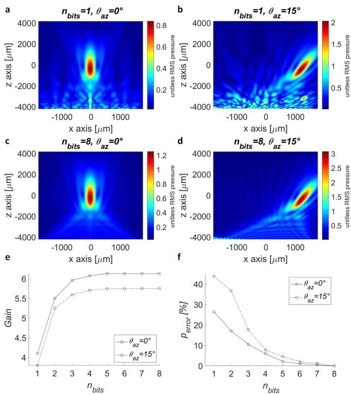
This article has been accepted for publication in a future issue of this journal, but has not been fully edited. Content may change prior to final publication. Citation information: DOI 10.1109/TBCAS.2021.3096722, IEEE
Transactions on Biomedical Circuits and Systems
> REPLACE THIS LINE WITH YOUR PAPER IDENTIFICATION NUMBER (DOUBLE-CLICK HERE TO EDIT) < 4
max pnbits p8bits (8)
perror 100
max p8bits
Fig. 4f shows the variation of perror for different nbits, where it
can be seen that for nbits greater than 6, negligible improvements
are obtained. Hence, nbits was set to 6, since it maximizes Gain
and minimizes acoustic wave constructive interferences at
locations outside of the focal spot.
III. ULTRASOUND TRANSDUCER MATERIAL
The most common types of transducers used in ultrasound
phased arrays are either piezoelectric, in the form of bulk
transducers or piezoelectric micromachined ultrasound
transducers (pMUTs), or capacitive micromachined ultrasound
transducers (cMUTs). Piezoelectric transducers are still the
most widely used transducer type. In the form of bulk
transducers, they typically use the inverse piezoelectric effect
of PZT ceramics, which convert an applied AC signal into
thickness mode vibration, generating acoustic waves. PZT is
characterized by high Stx, high quality factor (Q), and a high
acoustic mismatch with soft tissue, typically requiring an
acoustic matching layer to increase the transmission efficiency
and an acoustic backing layer if increased bandwidth is
Fig. 4. Influence of timing resolution on the focal spot properties. a,b required, such as in the case of ultrasound imaging applications.
simulated beam profiles of an ultrasound wave with N of 5 mm generated by In pMUTs, on the other hand, transduction is performed by
a 26x26 2D ultrasound array with 1 bit (a) and 8 bit (b) of timing resolution. application of an AC signal across a suspended piezoelectric
c,d, influence of timing resolution in fg (c) and in the normalized beam profile
flexural membrane, typically of PZT or aluminum nitride (AlN)
pratio (d).
[34]. Since pMUT membranes are softer than bulk PZT, they
error, N was set to 26 x 26. Increasing N further produced inherently increase the acoustic matching with soft tissue
negligible improvements in the simulated Zm while increasing without requiring acoustic matching layers. However, the Stx of
the total number of transducers and circuit area, which, for a pMUTs is still much lower than of bulk PZT transducers [28,
given total power budget, leads to a tighter power/channel ratio. 34], making pMUTs more appropriate in sensing applications
All of the abovementioned trade-offs assume that Tmin is low [35]. Similarly to pMUTs, cMUTs also operate with suspended
enough to generate the precise phasing for focal spot flexural membranes, and have the advantage of using
generation. As lower Tmin requires higher timing resolution in membrane materials compatible with the CMOS manufacturing
the transmitting circuit, and, consequently, higher circuit area, process, such as silicon nitride. Traditionally, cMUTs are
the effect of Tmin on the focal spot properties must also be characterized with a lower Stx when compared to PZT [27];
determined. The number of bits of precision (nbits) was defined however, they have a much lower Q and, as pMUTs, higher
as: acoustic matching with soft tissue [36]. For ultrasound imaging
1 (7) applications, the lower Q of cMUTs leads to great advantage
nbits log 2 over piezoelectric transducers, since it allows for an inherently
fUS Tmin better axial resolution. On the other hand, for the applications
k-wave simulations were performed for a 26×26 array
configured for a geometric Zm of 5 mm, θYZ of 0° and θXZ of 0° targeted in this work, the high Stx of PZT leads to the generation
and 15° and and nbits spanning from 1 to 8 bits. The beam of higher acoustic intensities at the focal spot, while its higher
profile for the extreme cases (nbits = 1 and nbits = 8) are shown Q enables higher power efficiency in the acoustic transmission
in Fig. 4a-d, where an increase of approximately 30% in the [15].
Gain is observed for 8 bits, with the trend shown in Fig. 4c. In Bulk PZT transducers are still preferable to cMUTS when
addition, with nbits equal to 1, unwanted acoustic wave high Stx and Q are required. While it has been shown that
constructive interferences appear in locations outside of the cMUTs can be optimized to have a Stx similar to that of bulk
focal spot (Fig. 4a,b). These can lead to unwanted effects, such PZT [37] by using substrate-embedded springs, if PZT is
as powering up an incorrect device in a distributed implantable acoustically matched with soft tissue, its effective Stx increases
device scheme, or interact with unwanted neuronal circuits. beyond that of cMUTs [38]. Also, advanced ceramic-based
These unwanted effects where quantified by the error of the piezoelectric materials such as Lead Magnesium Niobate/Lead
maximum of the pressure difference between the beam profile Titanate (PMN-PT) provide an opportunity to boost the
for varying nbits (pnbits) and the beam profile for 8 bits (p8bits), effective Stx approximately 3 to 5 times compared with PZT
which corresponds to the focal spot pressure: [39].
1932-4545 (c) 2021 IEEE. Personal use is permitted, but republication/redistribution requires IEEE permission. See http://www.ieee.org/publications_standards/publications/rights/index.html for more information.
Authorized licensed use limited to: Columbia University Libraries. Downloaded on July 16,2021 at 19:59:11 UTC from IEEE Xplore. Restrictions apply.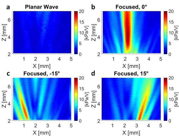
This article has been accepted for publication in a future issue of this journal, but has not been fully edited. Content may change prior to final publication. Citation information: DOI 10.1109/TBCAS.2021.3096722, IEEE
                                                                                        Transactions on Biomedical Circuits and Systems
          > REPLACE THIS LINE WITH YOUR PAPER IDENTIFICATION NUMBER (DOUBLE-CLICK HERE TO EDIT) <                                                                                                            5

           Fig. 5. IC with transmit beamformer for 2D ultrasound phased arrays. a, block diagram of IC showing the coarse phase control and the transmit channels composed
           by the fine phase control and driver. b,c, building blocks of the DLL: phase detector and charge pump(b), delay line element (c). d, transistor level schematic of
           phase interpolator used in the fine phase control section of each transmit channel. e, transistor level schematic of the transmit channel driver, composed by a level
           shifter and a class-D amplifier.

                                                                                                               bias the current-starved voltage-controlled inverter in the delay
                                              IV. IC DESIGN                                                    elements, as shown in Fig. 5c. Each current-starved inverter in
             The IC electronics (Fig. 5a) transform an externally supplied                                     series with a standard inverter in the six-element delay line
          input clock signal (CLK0) into 26 × 26 driving signals, each one                                     consumes a dynamic current of 16 µA in the locked state at 10
          with the appropriate phase to implement a transmit beamformer                                        MHz. To minimize the loading differences between the delay
          [29]. The IC was designed in two separate sections, a central                                        element outputs, a dummy delay element is added at the last
          coarse phase control unit, and an array of 26 × 26 transmit                                          stage of the delay line. CLK0 and CLK1-6 are fed into the
          channels, featuring a fine phase control unit and a driver [25].                                     transmit channel array and to minimize clock skew, a clock
          This solution provides a balance between having a central                                            buffer tree is designed using a distributed buffer scheme.
          beamforming unit, which would create a complex routing                                                  The fine-phase control circuit (Fig. 5d) includes a register
          problem, and having the beamforming circuit in each channel,                                         where the 6 bits corresponding to the phase are stored (d5-0).
          which would require more circuit area per channel and reduce                                         Two input multiplexers select two clocks with consecutive
          the scalability of the operating frequency. To configure all the                                     phases (CLKα and CLKβ) using d4-2, and uses a phase
          internal registers with all the beamforming phase information,                                       interpolator to generate an output differential signal with a fine-
          a data loader digital block was also included.                                                       tuned phase [40]. d1-0 is thermometer-coded to control the tail
             The coarse phase control unit is implemented by a delay                                           current of differential pairs M7-14. The tail current value is 43
          locked loop (DLL) with the architecture shown in Fig. 5a. By                                         µA, with an LSB of 10.75 µA, which corresponds to a phase
          applying an input CLK0, the DLL generates six output clocks                                          resolution of 7.5° and Tmin of 2.08 ns. Since the DLL outputs
          with an incremental 30° phase difference to CLK0 (CLK1-6),                                           only cover the phases from 0° to 180°, the phase interpolator
          from 30° up to 180°, which at 10 MHz represents a time                                               expands the phase map from 0° to 360°. This is done through
          resolution of 8.3 ns. The phase detector supplies the inputs to                                      transistors M3-6, controlled by d5 to steer the tail current between
          the charge pump (Fig. 5b). The charge pump biasing current is                                        two sets of differential pairs, one set for an output phase in the
          6.4 µA, and with a load capacitance of 7.2 pF, the DLL locks                                         quadrants from 0° to 180° (M7,8 and M11,12), and the other set
          the phase of CLK0 and CLKπ (unbuffered version of CLK6 as                                            for an output phase-shifted to the quadrants from 180° to 360°
          seen in Fig. 5a) in less than 1 µs, for a frequency of 10 MHz.                                       (M9,10 and M13,14).
          The output of the charge pump (Vctrl) is converted into biasing                                         All of the phase control circuitry operates at a 1.8-V power
          voltages VCP and VCN by using the replica biasing circuit, which                                     supply. A driver circuit in each transmit channel, consisting of

  1932-4545 (c) 2021 IEEE. Personal use is permitted, but republication/redistribution requires IEEE permission. See http://www.ieee.org/publications_standards/publications/rights/index.html for more information.
                    Authorized licensed use limited to: Columbia University Libraries. Downloaded on July 16,2021 at 19:59:11 UTC from IEEE Xplore. Restrictions apply.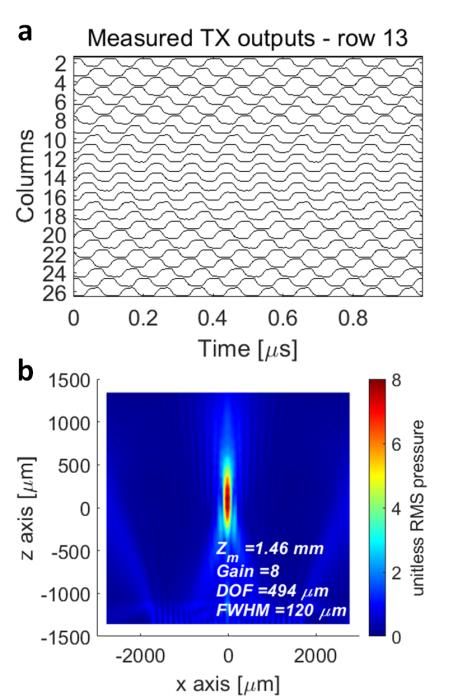
This article has been accepted for publication in a future issue of this journal, but has not been fully edited. Content may change prior to final publication. Citation information: DOI 10.1109/TBCAS.2021.3096722, IEEE
Transactions on Biomedical Circuits and Systems
> REPLACE THIS LINE WITH YOUR PAPER IDENTIFICATION NUMBER (DOUBLE-CLICK HERE TO EDIT) < 6
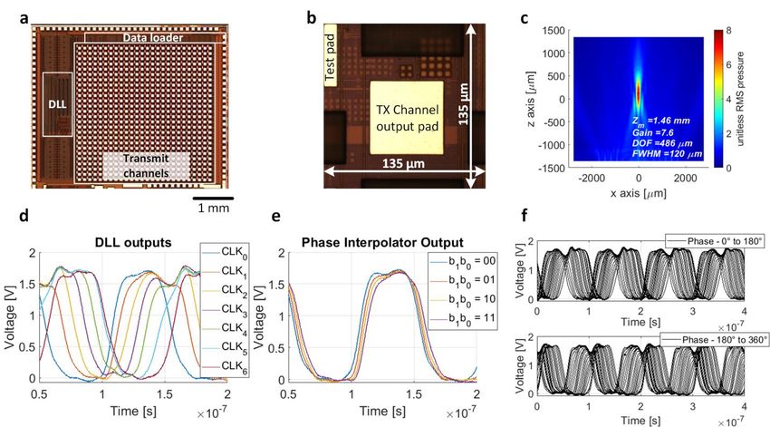
Fig. 6. Electrical experimental characterization of the IC. a, microphotograph of fabricated IC, with an area of 4 mm × 5 mm, and a transmit array area of 3.75
mm × 3.75 mm. b, microphotograph of a single transmit channel. c, simulated beam profile for a 26 × 26 ultrasound transducer array with a geometrical focal spot
N of 2 mm, with ideal acoustic signals. d, DLL output signals with a 10-MHz CLK generated by the FPGA as the DLL input. e, output of the phase interpolator
of ch0 with the 4 possible output phases. CLKα and CLKβ digital configured to be equal to the DLL outputs corresponding to CLK0 and CLK1. f, complete phase
sweep for ch0.
a level shifter and Class-D amplifier, boosts the voltage up to 5 DLL. The average time delay between the coarse phase control
V to drive the transducer (Fig. 5e). outputs was 8.76 ns with a standard deviation of 1.7 ns. It is of
note that this measurement also takes into account the clock
V. ELECTRICAL CHARACTERIZATION buffer network that connects the outputs of the coarse phase
control to each transmission channel. The phase interpolator
The IC, a microphotograph of which is shown in Fig. 6a as
outputs of ch0 (Fig. 6e) represent the phase interpolation
manufactured in a TSMC 180 nm 1.8/5V process, occupies an
between the first two outputs of the DLL, CLK0 and CLK1,
area of 5 mm × 4 mm. The transmit channel was designed in a
selected with d5-2 set to 0. The results shown in Fig. 6e reveal
2D array with a d of 135 µm (Fig. 6b), hence, some degree of
an average delay resolution of 1.6 ns with a standard deviation
grating lobes were expected, however, k-wave simulations
of 0.28 ns, which, again, includes any possible clock skew from
using a 26x26 array of acoustic sources with a d of 135 µm
the distributed clock buffer tree.
revealed that the peak pressure of grating lobes is negligible
To analyze the transmitter channel performance across the
when compared with the pressure at the focal spot (Fig. 6c). The
array, 16 channels equally spaced across the array were
die was wirebonded to a custom PCB socket and encapsulated
measured by sweeping the input phase control bits. The results
with a UV curable epoxy. The PCB socket connects to a test
for the first measured channel are shown in Fig. 6f, split
motherboard, which features a Spartan-6 FPGA development
between 0° to 180° and 180° to 360°. The delay transfer
board (Opal Kelly XEM6310). The measurement results
presented here were obtained by supplying the IC with a 10-
MHz input CLK, divided in the FPGA from a 100 MHz low-
jitter oscillator (0.5 psRMS), and by direct probing the output
pads of each transmitter connected to the corresponding driver
circuit. Given the jitter of the input CLK being 3 orders of
magnitude lower than Tmin, we have neglected its effect. For
simplicity, the high voltage supply of the IC is shared with the
core supply voltage of 1.8 V.
We first characterized the output timing characteristics of the
coarse and fine phase control of the first channel in the array
(ch0), by sweeping the corresponding phase control bits. The Fig. 7 delay transfer function for 16 channels equally spread across the array. a,
outputs of the coarse phase control were recorded (Fig. 6d) at average (red) and standard deviation (blue) values for the measured 16 channels.
b, average (red) and standard deviation (blue) values of INL and DNL of the
the ch0 output with bits d5,1,0 set to 0 to select the outputs of the
delay transfer function shown in (a)
1932-4545 (c) 2021 IEEE. Personal use is permitted, but republication/redistribution requires IEEE permission. See http://www.ieee.org/publications_standards/publications/rights/index.html for more information.
Authorized licensed use limited to: Columbia University Libraries. Downloaded on July 16,2021 at 19:59:11 UTC from IEEE Xplore. Restrictions apply.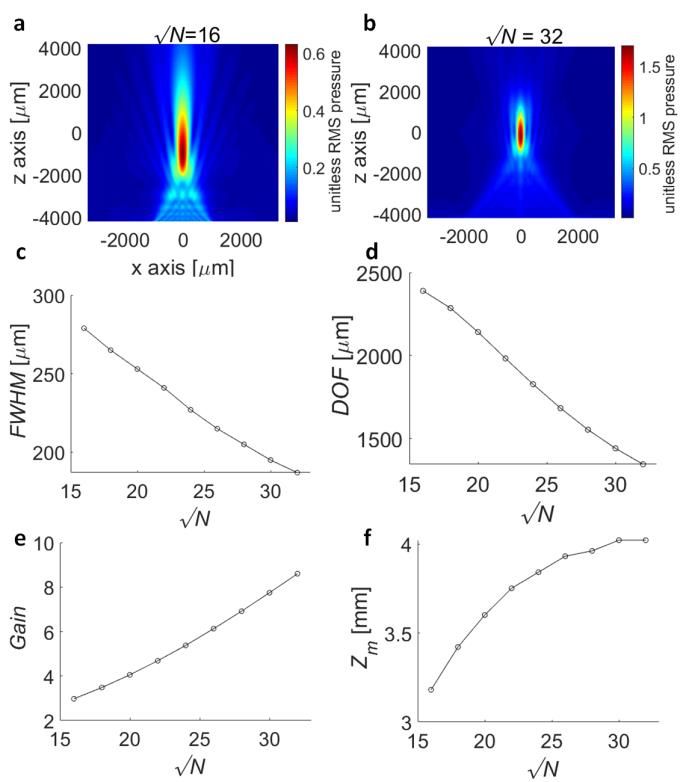
This article has been accepted for publication in a future issue of this journal, but has not been fully edited. Content may change prior to final publication. Citation information: DOI 10.1109/TBCAS.2021.3096722, IEEE
                                                                                        Transactions on Biomedical Circuits and Systems
          > REPLACE THIS LINE WITH YOUR PAPER IDENTIFICATION NUMBER (DOUBLE-CLICK HERE TO EDIT) <                                                                                                            7

                                                                                                               from the DLL outputs to transmitter array, had no effects on
                                                                                                               FWHM and Zm, and negligible effects on DOF and Gain, with
                                                                                                               a difference between simulations with ideal and measured
                                                                                                               signals of only 1.6% and 5%, respectively.
                                                                                                                  The IC was also characterized for operating frequencies from
                                                                                                               7 MHz to 14 MHz, with 1 µs PD measured at the output of ch0,
                                                                                                               as shown in Fig. 9a. The ability of the IC to operate at
                                                                                                               frequencies around the central frequency of 10 MHz adds the
                                                                                                               flexibility of interfacing with ultrasound transducers with
                                                                                                               slightly different resonance frequencies. In the case of bulk
                                                                                                               piezoelectric transducers such as PZT, the resonance frequency
                                                                                                               is directly related to the material thickness, which is dependent
                                                                                                               on manufacturing tolerances. PD can be arbitrarily set by
                                                                                                               setting the ON time of an enable signal, which is connected to
                                                                                                               all transmit channels, as shown in the measurement of Fig. 9b.
                                                                                                               Here, ch0 was measured with a pulse repetition frequency (PRF)
                                                                                                               of 10 kHz and duty cycles of 1%, 10% and 50%, which
                                                                                                               correspond to PD of 1 µs, 10 µs and 50 µs, respectively. By
                                                                                                               decreasing the PRF, PD values in the millisecond range can be
                                                                                                               obtained, however, requiring careful monitoring of heat
                                                                                                               dissipation.
          Fig. 8 Beam profile simulation using measured electrical signals as acoustic
                                                                                                                           VI. ULTRASOUND TRANSDUCER INTEGRATION
          sources for a focal depth of 5 mm. a Signals of row 13. b, Beam profile
                                                                                                                 The IC described here requires direct integration of
          function for all the measured channels is displayed in Fig. 7a,                                      ultrasound transducers with a footprint matched to the output
          revealing a monotonic characteristic. Further analysis of the                                        pads of the array of transmitters (Fig. 6b). For that reason, we
          data of Fig. 7a reveals an average resolution of 2.12 ns, which                                      have developed an integration method for a 2D array of PZT
          is close to the designed value of 2.08 ns, with a standard                                           transducers directly on top of the IC [25, 41] and illustrated in
          deviation of 0.94 ns. The integral nonlinearity (INL) and                                            Fig. 10. The fabrication method follows a subtractive process,
          differential nonlinearity (DNL) of the transfer curve of Fig. 7a                                     starting with a commercially available 7.24 × 7.24 cm2 sheet of
          are shown in Fig. 7b. While the average DNL is less than 1 LSB,                                      pre-polled 267-µm-thick PZT5A (piezo.com). The measured
          which guarantees monotonicity, there is a larger INL, of up to                                       charge sensitivity of the bulk PZT5A was 360 pC/N (d33 meter,
          3 LSBs.                                                                                              Piezotest). Contacts (10 nm of Cr followed by 100 nm of Au)
             To understand the impact of the INL of the designed system                                        were patterned on both sides of the sheet by using lift-off
          in its ability to perform beam steering and on the focal spot                                        photolithography and e-beam evaporation (Fig. 11a). The
          characteristics, the IC was programmed to generate driving                                           PZT5A sheet was then cut into small chips matching the
          signals corresponding to N of 2 mm with a steering angle of 0°,                                      transmit array dimensions of 3.75 mm × 3.75 mm using a dicing
          and all the outputs were measured for a duration of 1 µs, as                                         saw process. Afterward, a PZT5A chip is pre-diced from one
          illustrated in Fig. 8a for row 13. Similarly to the simulation                                       side by about 20% of its thickness using the same dicing saw
          done in Fig. 6c, a k-wave simulation was then performed for a                                        process with a blade thickness of 50 µm, resulting in kerfs with
          26 × 26 2D array of acoustic sources, with 135 µm pitch, 10                                          a width of approximately 55 µm. Following this step, the
          MHz operating frequency, using the signals measured from the                                         CMOS chip I/O pads are protected with a thin layer of
          IC as acoustic sources. The simulated beam profile is shown in                                       photoresist. Afterwards, an anisotropic conductive film (ACF,
          Fig. 8b, including the calculated focal spot parameters.                                             TFA220-8, H&S High Tech) was tacked to the surface of the
          Comparing with the simulation with ideal sources of Fig. 6c, it
          can be seen that the non-linearity of the transmitter channel
          transfer function, and other nonidealities such as clock skew

                                                                                                                 Fig. 10 Fabrication flow including PZT contact deposition (i) and patterning
                                                                                                                 (ii), back side dicing (iii), adhesion to the CMOS chip using an anisotropic
          Fig. 9 Output of ch0 for different input CLK frequencies (a) and duty cycles                           conductive film (ACF) (iv), PZT top side dicing (v), kerf filling (vi) and top
          (PD) (b)                                                                                               metallization (vii)

  1932-4545 (c) 2021 IEEE. Personal use is permitted, but republication/redistribution requires IEEE permission. See http://www.ieee.org/publications_standards/publications/rights/index.html for more information.
                    Authorized licensed use limited to: Columbia University Libraries. Downloaded on July 16,2021 at 19:59:11 UTC from IEEE Xplore. Restrictions apply.
This article has been accepted for publication in a future issue of this journal, but has not been fully edited. Content may change prior to final publication. Citation information: DOI 10.1109/TBCAS.2021.3096722, IEEE
                                                                                        Transactions on Biomedical Circuits and Systems
          > REPLACE THIS LINE WITH YOUR PAPER IDENTIFICATION NUMBER (DOUBLE-CLICK HERE TO EDIT) <                                                                                                            8

                                                                                                               were individually verified to have no effects on the
                                                                                                               piezoelectric properties of the PZT material.

                                                                                                                    VII. ULTRASOUND EXPERIMENTAL CHARACTERIZATION
                                                                                                               To validate both the fabrication method and the interface
                                                                                                               between the IC and the 2D ultrasound transducer array, an
                                                                                                               ultrasound experimental test setup was implemented (Fig. 12a).
                                                                                                               The IC was encapsulated and interfaced as described in section
                                                                                                               VI, with the high voltage supply shared with the 1.8 V core
                                                                                                               supply, for simplicity. The PCB socket with the fabricated
                                                                                                               device was immersed into a 3D-printed container filled with
                                                                                                               distilled water and connected to the test motherboard. A
                                                                                                               hydrophone (HGL-0200 – OndaCorp), connected to an
         Fig. 11 Photographs of the fabrication of 2D PZT array on top of CMOS chip.                           amplifier with 20 dB of gain (AG-2010 - OndaCorp), is
         a, PZT sheet with Cr/Au contacts. b, overlay of the CMOS and PZT released                             attached to a three-axis motorized stage (MTS50/M-Z8 –
         chip images for alignment. c, top view of the integrated chip after PZT top dice                      Thorlabs) and immersed in the distilled water bath at the center
         dicing. d, test pads on the CMOS chip revealing fully individualized PZT                              of the array. The hydrophone has an aperture of 200 µm and an
         structures. e, chip after filling the PZT pillar kerfs with an epoxy through
                                                                                                               acceptance angle of 100°, with the amplifier ensuring a flat
         capillarity. f, top level metallization (Cu), wirebonding and encapsulation in a
         custom test PCB.                                                                                      frequency response up to 40 MHz. The stage controller outputs
                                                                                                               a digital signal that is high when the stage is moving, which is
          CMOS chip, centered with the array of transmitter output pads.                                       connected to an oscilloscope (Keysight MSO-X 4054A) to
          By using a chip bonding tool (Fineplacer Lambda, Finetech),                                          provide synchronization between the hydrophone readout
          the CMOS and PZT5A chips are aligned with sub-µm precision                                           signal and its position. The IC transmitters are controlled by an
          (Fig. 11b), with the PZT5A pre-diced layer facing the CMOS                                           enable signal (TXenable), which is used as the trigger signal for
          chip surface. Given the conductive particle density of the ACF                                       the hydrophone readout. The stage controller, oscilloscope, and
          of 40000 pcs/mm2, this leads to approximately 100 conductive                                         FPGA are connected to a computer by USB, where a graphical
          particles for the CMOS pad dimensions of 50 x 50 µm2. Hence,                                         user interface is used to control all the components of the
          a lower precision alignment can be tolerated, as long as the                                         measurement. A photograph of part of the measurement setup
          higher contact resistance and lower current density does not                                         is shown in Fig. 12b.
          lead to a decreased voltage across the PZT5A transducer; both
          chips are then bonded by thermo-compression, with a force of                                            The resonance frequency of the transducer was obtained by
          150 N and 175 °C for 15 seconds. Both temperature and                                                measuring the frequency of maximum output pressure. This
          pressure were calibrated to ensure that a monolayer of                                               was done by sweeping the driving frequency of the transducers
          conductive particles is created at the interface between the                                         and measuring the output pressure of the array with the
          PZT5A and the CMOS chip pads.                                                                        hydrophone, with the result shown in Fig. 12c. The maximum
            The PZT5A chip was then diced from the top with the 50-µm-                                         pressure was achieved for a 8.4 MHz, which was set as the
          thick blade going through 90% of the original thickness, leading                                     working frequency for the next steps in the device
          to individual PZT5A pillars without damaging the CMOS chip                                           characterization. The IC was then programmed to output a
          surface. The actual pillar kerfs were measured to be                                                 planar wave, with all transmitter channels generating the same
          approximately 65 µm. The resulting fully diced transducers are                                       driving signal and with a PRF of 10 kHz and a duty cycle of
          shown in Fig. 11c, with Fig. 11d showing the CMOS chip                                               1%, corresponding to PD of 1 µs. To decouple ultrasound
          surface, where the transmitter test pads are seen in the PZT5A                                       waves from any capacitive coupling from the IC driving signals
          array kerfs. From Fig. 11c, only two transducers are missing in                                      and the hydrophone tip electrode, the hydrophone was placed 2
          the bottom right corner, which results in a yield of 99.7 %.                                         mm away from the fabricated device, which corresponds to
            Finally, the pillar kerfs are filled with an epoxy to give                                         approximately 1.3 µs of the ultrasound propagation time (larger
          mechanical stability to the array, and to serve as a supporting                                      than PD). The motorized stage was programmed to scan an area
          structure for the PZT5A transducer array top contact, as seen in                                     of 5 mm x 5 mm in the XZ plane with steps of 100 µm, and the
          Fig. 11e. The ground connection for the 2D pillar array is                                           oscilloscope was programmed to record the peak to peak
          implemented by sputtering a 500-nm layer of copper on top of                                         acoustic pressure for each step of the hydrophone. The resulting
          the chip, as seen in Fig. 11f. By using a probe station                                              beam profile can be found in Fig. 13a, showing a uniform
          measurement system, it was confirmed that the ground plane                                           pressure level across the measured area below 10 kPa. The next
          was connected to all pillar structures. The final step consisted                                     step consisted of programming the IC to generate driving
          of lifting-off the photoresist covering the CMOS chip I/O pads,                                      signals corresponding to a focal depth of 5 mm, θYZ of 0°, and
          for subsequent wirebonding. The fully fabricated chip is also                                        θXZ of 0°, -15°, and 15°, following the same recording procedure
          shown in Fig. 11f, with the chip wirebonded and encapsulated                                         as with the planar wave test. The resulting beam profiles are
          to a custom test PCB. Given that the piezoelectric effects of                                        shown in Fig. 13b-d, clearly showing the generation of focused
          PZT5A can be degraded by exposure to high temperatures [42],                                         ultrasound waves. With a maximum focal pressure of
          all the fabrication steps involving temperatures above 100 °C                                        approximately 40 kPa with a 1.8 V driving voltage for the 0°
                                                                                                               case, and slightly less for the -15° and 15° angles, as expected.
                                                                                                               Since pressure scales linearly with the driving voltage, the

  1932-4545 (c) 2021 IEEE. Personal use is permitted, but republication/redistribution requires IEEE permission. See http://www.ieee.org/publications_standards/publications/rights/index.html for more information.
                    Authorized licensed use limited to: Columbia University Libraries. Downloaded on July 16,2021 at 19:59:11 UTC from IEEE Xplore. Restrictions apply.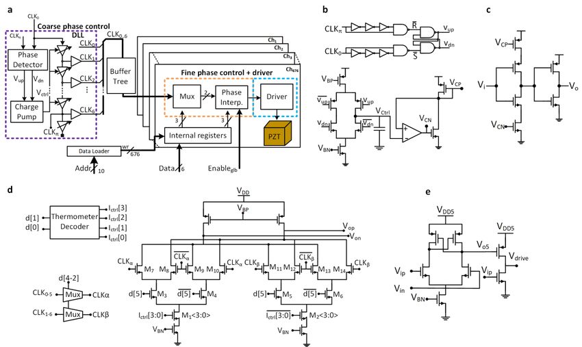
This article has been accepted for publication in a future issue of this journal, but has not been fully edited. Content may change prior to final publication. Citation information: DOI 10.1109/TBCAS.2021.3096722, IEEE
                                                                                        Transactions on Biomedical Circuits and Systems
          > REPLACE THIS LINE WITH YOUR PAPER IDENTIFICATION NUMBER (DOUBLE-CLICK HERE TO EDIT) <                                                                                                            9

           Fig. 12 Diagram of the ultrasound characterization setup (a), photograph of the test setup showing the motorized stage, hydrophone, container and chip (b).
           pressure variation with driving frequency (c).

          maximum driving voltage of 5 V leads to a maximum focal
          pressure of approximately 100 kPa. Higher focal pressure in the
          MPa range can be achieved if higher transducer driving
          voltages are used, if PMN-PT piezoelectric materials are
          employed instead of PZT5A, or if acoustic matching layers are
          added. Higher driving voltage can be used with standard low
          voltage CMOS processes by using stacked driving schemes
          [43], opposing to the area-consuming high-voltage DMOS
          transistors found in BCD processes. This further supports the
          high-frequency nature of this work, which requires low-area
          beamforming and driving circuits.
             The focal spot dimensions FWHM and DOF are 215 µm and
                                                                                                                Fig. 14 Overlapped beam profiles of the focused ultrasound waves,
          1.68 mm, respectively, which is larger than the values obtained                                       emphasizing the -3dB focal spot area.
          from simulations for the same L, fUS, and Zm, as seen in Fig. 3.
          This is also evident in Fig. 14, where the three measurements                                        µm and 400 µm, and DOF is approximately 4 mm. For θaz of -
          for focused waves are overlapped, showing only the                                                   15° and 15°, the measured FHWM is between 100 µm and 200
          measurements within -3-dB of the maximum pressure from                                               µm, which is in line with simulations shown in Fig. 3; however,
          each beam profile. Given the larger step size (100 µm) used in                                       DOF cannot be measured since it expands to a region closer to
          the hydrophone scan, a comparison cannot be made with the                                            the IC that cannot be accurately measured.
          same precision; however, for a θaz of 0°, FWHM is between 300                                           One possible source for this discrepancy is that not all of the
                                                                                                               elements in the transducer array are making electrical contact
                                                                                                               with the respective transmitter output pads, leading to a smaller
                                                                                                               active array area, which leads to larger values for FWHM and
                                                                                                               DOF. However, the measured Zm of 4 mm is close to the
                                                                                                               simulated value of 3.93 mm. Since the focus shift due to the
                                                                                                               Fresnel number of the ultrasound array depends on the active
                                                                                                               array area, a smaller active area would lead to a lower measured
                                                                                                               Zm, which is not observed. Given that the driving signals from
                                                                                                               the IC result in approximately equal simulated beam profiles
                                                                                                               when compared with the ideal case, as shown in Fig. 6c and Fig.
                                                                                                               8b, the more likely cause of the difference in focal spot
                                                                                                               dimensions is mechanical effects from the silicon substrate or
                                                                                                               the epoxy filling the array kerfs, which were not modeled.
                                                                                                               Further studies are required to provide more understanding of
                                                                                                               these effects, to further decrease the focal spot dimensions
                                                                                                               closer to the simulated values.

          Fig. 13 Measured ultrasound beam profile in the ZX plane, with planar wave
          (a), and with geometrical focus depth of 5 mm and steering angle of 0° (b), -
          15° (c) and 15°(d).

  1932-4545 (c) 2021 IEEE. Personal use is permitted, but republication/redistribution requires IEEE permission. See http://www.ieee.org/publications_standards/publications/rights/index.html for more information.
                    Authorized licensed use limited to: Columbia University Libraries. Downloaded on July 16,2021 at 19:59:11 UTC from IEEE Xplore. Restrictions apply.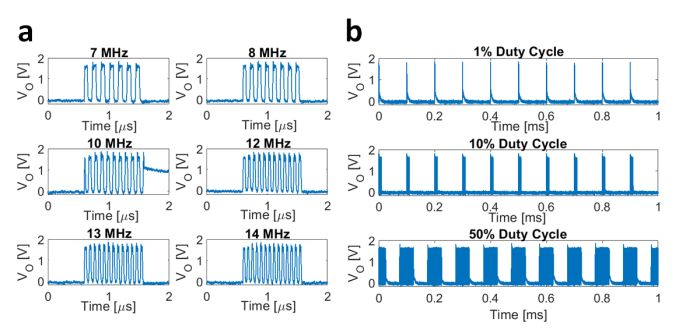
This article has been accepted for publication in a future issue of this journal, but has not been fully edited. Content may change prior to final publication. Citation information: DOI 10.1109/TBCAS.2021.3096722, IEEE
                                                                                        Transactions on Biomedical Circuits and Systems
          > REPLACE THIS LINE WITH YOUR PAPER IDENTIFICATION NUMBER (DOUBLE-CLICK HERE TO EDIT) <                                                                                                          10

                                                                                              TABLE I
                                                                          COMPARISON OF THIS WORK WITH THE STATE OF THE ART

                                                   [17]                           [20]                          [21]                           [24]                            This work
                   Application                   Imaging and                    Imaging                       Imaging                        Neuromodulation                Neuromodulation
                                                 neuromodulation                                                                                                            and wireless
                                                                                                                                                                            powering
                   CMOS Process                  Discrete                       0.25 µm HV                    0.18 µm LV                     0.18 µm HV                     0.18 µm LV
                   Transducer                    PZT                            CMUT                          PZT                            CMUT                           PZT
                   Integration                   NA                             Flip-chip                     Flip-Chip                      Flip-chip                      Flip-chip
                                                                                                  2                              2                       2
                   Chip area                     NA                             9.2x9.2 mm                    6.1x6.1 mm                     8x8 mm                         5x4 mm2
                   Power/channel                 NA                             4.5 mW                        0.27 mW                        NA                             1.5 mW
                   Center freq.                  1.3 MHz                        5 MHz                         5 MHz                          2 MHz                          8.4 MHz
                   # of Tx el.                   8 – 1D                         1024 – 2D                     64-off chip                    1024 – 2D                      676 – 2D
                   Full apert. TX                Yes                            Yes                           No                             Yes                            Yes
                   Arbitrary PD                  Yes                            No                            No                             Yes                            Yes
                   Focal pressure                1.6 MPa                        N/A                           300 kPa                        574 kPa                        40 kPa (up to 100
                                                                                                                                                                            kPa)
                   Focal depth                   3 cm                           N/A                           5 cm                           0.5 cm                         0.5 cm
                   Driving voltage               20 V                           55 V                          50 V                           60 V                           5V
                   Stx                           80 kPa/V                       N/A                           6 kPa/V                        9.5 kPa/V                      Up to 20 kPa/V
                                                                                                               patterned features in the PZT. This allowed us to dice 2D
                                          VIII. CONCLUSIONS                                                    ultrasound arrays of arbitrary number of elements with no risk
          We have presented an integrated 2D ultrasound phased-array                                           of damage to the IC.
          transmitter in CMOS that enables the use of miniaturized                                                By exploring the capabilities of phased arrays, IC design, and
          ultrasound devices for emerging applications such as ultrasound                                      direct integration of ultrasound transducers, we achieved the an
          neuromodulation and ultrasonic powering of implantable                                               integrated ultrasound transmitter device with 2D pixel pitch-
          devices. The first key innovation resided on the in depth                                            matched transmit beamforming at the full aperture, arbitrary PD
          analysis of the system-level design, by relating the ultrasound                                      and ultrasound frequency of 8.4 MHz, scalable up to 10 MHz
          focal spot properties, the 2D phased array geometry, and the                                         with negligible grating lobes. Comparing with other works
          required timing resolution for the transmit beamforming                                              (Table I), the combination of these feature is unique. An
          circuits. We often see ultrasound phased array systems with                                          increased ultrasound frequency translates into smaller
          hundreds and even more than one thousand channels, without                                           ultrasound focal spot volume, which is aligned with the ever-
          understanding the trade-offs of such systems. Our analysis                                           shrinking sizes of implantable devices and high-precision
          methodology allowed us to exactly specify the required                                               neuromodulation. Even though the focal spot pressure obtained
          ultrasound transducer geometry, frequency, and timing                                                in this work is lower than that presented in [17], adding an
          specifications of the beamforming electronics. The second                                            acoustic matching layer to the transducers presented in this
          innovation consisted of a mixed-signal continuous-wave                                               work can substantially improve the focal spot pressure, which
          beamforming approach for the driving circuits, opposing to the                                       can be even further increased by using area-efficient HV drivers
          more conventional digital approach [20, 24], which avoids the                                        and more advanced piezoelectric materials such as PMN-PT. If
          need of higher clock frequencies for the same timing resolution.                                     higher driving voltages and long pulse durations are used, heat
          In addition, it allowed for arbitrary pulse durations with a                                         dissipation must be monitored to ensure that temperature
          simple internal register controlled by a common enable signal.                                       remains within tolerable levels. Furthermore, the target
          This lead to a circuit implementation of a 2D array with full-                                       applications also require structural ultrasound imaging, which
          aperture pitch-matched transmitters towards a tighter pitch                                          was not the focus of this work. Since the imaging specifications
          between transmit channels and transducers. The third key                                             would require lower-frame rates compared to traditional
          innovation was seen in our direct integration method of PZT on                                       ultrasound imaging, we foresee that a sub-set of the transmitting
          top of the CMOS IC. Since the transducer pitch is inversely                                          channels could also include a receiver front-end to implement a
          proportional to the ultrasound frequency, the use of interposers                                     synthetic aperture scheme.
          or high-density conductive epoxies imposes a limitation in the                                          Thinning of the CMOS substrate will allow this device to be
          minimum transducer pitch. Here, we used a thin and low-                                              rendered mechanically flexible [44]. In this way, we can
          density ACF, consisting of 3 µm conducting particles allowing                                        envisage the emergence of wearable ultrasound patches for
          for down to sub-30 µm spacing. In our dicing process, since the                                      high-precision and non-invasive neuromodulation of peripheral
          ACF is too thin to protect the IC, we created a back-side/top-                                       nerves and for powering sub-mm implantable devices for both
          side dicing scheme, enabled by aligning top and back-side

  1932-4545 (c) 2021 IEEE. Personal use is permitted, but republication/redistribution requires IEEE permission. See http://www.ieee.org/publications_standards/publications/rights/index.html for more information.
                    Authorized licensed use limited to: Columbia University Libraries. Downloaded on July 16,2021 at 19:59:11 UTC from IEEE Xplore. Restrictions apply.
This article has been accepted for publication in a future issue of this journal, but has not been fully edited. Content may change prior to final publication. Citation information: DOI 10.1109/TBCAS.2021.3096722, IEEE
Transactions on Biomedical Circuits and Systems
> REPLACE THIS LINE WITH YOUR PAPER IDENTIFICATION NUMBER (DOUBLE-CLICK HERE TO EDIT) < 11
therapeutic and diagnostic applications, which will be focus of Microscopic Ultrasound Neuromodulation," IEEE Transactions on
Biomedical Circuits and Systems, pp. 1-1, 2019
future work.
[16] T. Choi, S. Bae, M. Suh, and J. Park, "A Soft Housing Needle
Ultrasonic Transducer for Focal Stimulation to Small Animal
Brain," Annals of Biomedical Engineering, 2019/12/13 2019
ACKNOWLEDGMENT [17] V. Pashaei, P. Dehghanzadeh, G. Enwia, M. Bayat, S. J. A. Majerus,
and S. Mandal, "Flexible Body-Conformal Ultrasound Patches for
We acknowledge the use of the Columbia Nano Initiative (CNI) Image-Guided Neuromodulation," IEEE Transactions on
cleanroom at Columbia University and the clean room of the Biomedical Circuits and Systems, pp. 1-1, 2019
[18] J. Lee et al., "A MEMS ultrasound stimulation system for
Advanced Science Research Center (ASRC) at City University
modulation of neural circuits with high spatial resolution in vitro,"
of New York. This work was supported in part by the Defense Microsystems & Nanoengineering, vol. 5, no. 1, p. 28, 2019/07/15
Advanced Research Projects Agency (DARPA) under 2019
Contracts HR0011-15-2-0054 and N66001204075, and [19] C. Wang et al., "Monitoring of the central blood pressure waveform
via a conformal ultrasonic device," Nature Biomedical Engineering,
Cooperative Agreement D20AC00004.
vol. 2, no. 9, pp. 687-695, 2018/09/01 2018
[20] A. Bhuyan et al., "Integrated Circuits for Volumetric Ultrasound
Imaging With 2-D CMUT Arrays," IEEE Transactions on
REFERENCES Biomedical Circuits and Systems, vol. 7, no. 6, pp. 796--804, 2013
[21] C. Chen et al., "A Front-End ASIC With Receive Sub-array
Beamforming Integrated With a 32 x 32 PZT Matrix Transducer for
[1] W. Legon et al., "Transcranial focused ultrasound modulates the 3-D Transesophageal Echocardiography," IEEE Journal of Solid-
activity of primary somatosensory cortex in humans," Nat Neurosci, State Circuits, pp. 1--13, 2017
vol. 17, no. 2, pp. 322-9, Feb 2014 [22] D. Wildes et al., "4-D ICE: A 2-D Array Transducer With Integrated
[2] J. Vion-Bailly, W. A. N’Djin, I. M. Suarez Castellanos, J.-L. ASIC in a 10-Fr Catheter for Real-Time 3-D Intracardiac
Mestas, A. Carpentier, and J.-Y. Chapelon, "A causal study of the Echocardiography," IEEE Transactions on Ultrasonics,
phenomenon of ultrasound neurostimulation applied to an in vivo Ferroelectrics, and Frequency Control, vol. 63, no. 12, pp. 2159-
invertebrate nervous model," Scientific Reports, vol. 9, no. 1, p. 2173, 2016
13738, 2019/09/24 2019 [23] R. Wodnicki et al., "Co-Integrated PIN-PMN-PT 2-D Array and
[3] W. J. Tyler, "The mechanobiology of brain function," Nature Transceiver Electronics by Direct Assembly Using a 3-D Printed
Reviews Neuroscience, vol. 13, no. 12, pp. 867-878, 2012/12/01 Interposer Grid Frame," IEEE Transactions on Ultrasonics,
2012 Ferroelectrics, and Frequency Control, vol. 67, no. 2, pp. 387-401,
[4] D. Folloni et al., "Manipulation of Subcortical and Deep Cortical 2020
Activity in the Primate Brain Using Transcranial Focused [24] C. Seok, O. Adelegan, A. O. Biliroglu, F. Y. Yamaner, and O.
Ultrasound Stimulation," Neuron, vol. 101, no. 6, pp. 1109-1116.e5, Oralkan, "A 2D Ultrasonic Transmit Phased Array Based on a
2019/03/20/ 2019 32x32 CMUT Array Flip-Chip Bonded to an ASIC for Neural
[5] M. E. Downs, S. A. Lee, G. Yang, S. Kim, Q. Wang, and E. E. Stimulation," in IEEE International Ultrasonics Symposium (IUS),
Konofagou, "Non-invasive peripheral nerve stimulation via focused 2020 2020: IEEE.
ultrasound in vivo " Physics in Medicine and Biology, vol. 63, no. 3, [25] T. Costa, C. Shi, K. Tien, and K. L. Shepard, "A CMOS 2D
p. 035011, 2018 Transmit Beamformer With Integrated PZT Ultrasound Transducers
[6] Y. Liu et al., "Bidirectional Bioelectronic Interfaces: System Design For Neuromodulation," in 2019 IEEE Custom Integrated Circuits
and Circuit Implications," IEEE Solid-State Circuits Magazine, vol. Conference (CICC), 14-17 April 2019 2019, pp. 1-4, doi:
12, no. 2, pp. 30-46, 2020 10.1109/CICC.2019.8780236.
[7] D. Seo, J. M. Carmena, J. M. Rabaey, E. Alon, and M. M. Maharbiz, [26] W. Arden, M. Brillouet, P. Cogez, M. Graef, B. Huizing, and R.
"Neural Dust: An Ultrasonic, Low Power Solution for Chronic Mahnkopf, "More-than-Moore, White Paper," [Online].Available:
Brain-Machine Interfaces," arXiv.org, vol. q-bio.NC, no. April, http://www.itrs2.net/uploads/4/9/7/7/49775221/irc-itrs-mtm-
2013 v2_3.pdf, 2019.
[8] D. Seo et al., "Wireless Recording in the Peripheral Nervous System [27] I. Wygant, "A comparison of CMUTs and piezoelectric transducer
with Ultrasonic Neural Dust," Neuron, vol. 91, no. 3, pp. 529--539, elements for 2D medical imaging based on conventional simulation
2016 models," in IEEE International Ultrasonics Symposium, 2011.
[9] B. C. Johnson et al., "StimDust: A 6.5mm3, wireless ultrasonic [28] E. Ledesma et al., "Squared PMUT with Enhanced Pressure
peripheral nerve stimulator with 82% peak chip efficiency," in IEEE Sensitivities," Proceedings, vol. 2, no. 13, p. 925, 2018
Custom Integrated Circuits Conference (CICC), 2018, pp. 1--4. [29] L. Azar, Y. Shi, and S. C. Wooh, "Beam focusing behavior of linear
[10] Y. Zhang and K. L. Shepard, "A 0.6-mm2 Powering and Data phased arrays," NDT and E International, vol. 33, no. 3, pp. 189--
Telemetry System Compatible with Ultrasound B-Mode Imaging 198, 2000
for Freely Moving Biomedical Sensor Systems," in 2019 IEEE [30] S.-C. Wooh and Y. Shi, "Optimization of Ultrasonic Phased
Custom Integrated Circuits Conference (CICC), 14-17 April 2019 Arrays," in Rev. Prog. Quant. Nondestructive Eval. : Springer,
2019, pp. 1-4, doi: 10.1109/CICC.2019.8780205. Boston, MA., 1998, pp. 883-890.
[11] J. Charthad et al., "A mm-Sized Wireless Implantable Device for [31] M. C. Ziskin, "Fundamental physics of ultrasound and its
Electrical Stimulation of Peripheral Nerves," IEEE Transactions on propagation in tissue," RadioGraphics, vol. 13, no. 3, pp. 705-709,
Biomedical Circuits and Systems, vol. 12, no. 2, pp. 257--270, 2018 1993
[12] J. Vo, T. C. Chang, K. I. Shea, M. Myers, A. Arbabian, and S. [32] k-Wave. (2009).
Vasudevan, "Assessment of miniaturized ultrasound-powered [33] K. Lou, S. Granick, and F. Amblard, "How to better focus waves by
implants: an in vivo study," Journal of Neural Engineering, vol. 17, considering symmetry and information loss," Proceedings of the
no. 1, p. 016072, 2020 National Academy of Sciences, vol. 115, no. 26, p. 6554, 2018
[13] C. Shi, T. Costa, J. Elloian, Y. Zhang, and K. L. Shepard, "A 0.065- [34] Y. Qiu et al., "Piezoelectric Micromachined Ultrasound Transducer
mm(3) Monolithically-Integrated Ultrasonic Wireless Sensing Mote (PMUT) Arrays for Integrated Sensing, Actuation and Imaging,"
for Real-Time Physiological Temperature Monitoring," IEEE Trans Sensors, vol. 15, no. 4, 2015
Biomed Circuits Syst, vol. 14, no. 3, pp. 412-424, Jun 2020 [35] X. Jiang et al., "Monolithic ultrasound fingerprint sensor,"
[14] C. Shi et al., "Application of a sub–0.1-mm3 implantable mote for Microsystems & Nanoengineering, vol. 3, no. 1, p. 17059,
in vivo real-time wireless temperature sensing," Science Advances, 2017/11/20 2017
vol. 7, no. 19, p. eabf6312, 2021 [36] A. S. Ergun, G. G. Yaralioglu, and B. T. Khuri-Yakub, "Capacitive
[15] H. S. Gougheri, A. Dangi, S. Kothapalli, and M. Kiani, "A Micromachined Ultrasonic Transducers: Theory and Technology,"
Comprehensive Study of Ultrasound Transducer Characteristics in Journal of Aerospace Engineering, vol. 16, no. 2, pp. 76-84, 2003
1932-4545 (c) 2021 IEEE. Personal use is permitted, but republication/redistribution requires IEEE permission. See http://www.ieee.org/publications_standards/publications/rights/index.html for more information.
Authorized licensed use limited to: Columbia University Libraries. Downloaded on July 16,2021 at 19:59:11 UTC from IEEE Xplore. Restrictions apply.You can also read